


NanoRacer High-Speed AFM
Bruker Nano GmbH
Developers: Tilo Jankowski, Detlef Knebel, and Torsten Jähnke
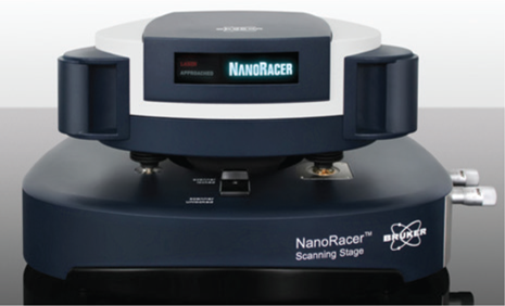
The NanoRacer high-speed atomic force microscope (AFM) has a video rate scanning speed of 50 frames/sec. The 5 kHz line-rate scanning is more than three orders of magnitude faster than typical AFM instruments. High-precision electronics and enhanced accuracy of positioning sensors enable closed-loop sample scanning on all three axes. These factors contribute to reduction of drift, enable routine observation of atomic defects, and reach resolution at sub-molecular levels. Surveying molecular events with a temporal resolution of 20 ms is possible with an 8 MHz bandwidth detector. Scan speed limitations were reduced using high-bandwidth processing electronics, a custom high-speed power amplifier, and advanced algorithms for scanner control and feedback loop error correction. Dynamic proportional-integral-derivative (PID) control eliminates feedback saturation errors, improves the tip-sample force control, and ensures stable successive imaging on soft and fragile samples. Fully automated alignment and calibration ensure fast cantilever drive and minimal perturbance of delicate samples. Laser excitation in the near-infrared range is optional for photosensitive and thermally unstable samples. Fast electronics and advanced algorithms ensure short feedback response times for the high-resonance 180 kHz z-scanner, typically faster than the cantilever resonance.
These technological improvements allow real-time visualization of dynamic processes taking place on the millisecond scale, enabling researchers to gain better understanding of complex biological systems and molecular mechanisms. New workflow-based software, suitable for multi-user environments, produces higher throughput and allows more experiments per day. The multi-level user-friendly interface features optional guidance and context-sensitive onscreen assistance; operators, irrespective of experience level, can focus on performing novel measurements rather than troubleshooting technical challenges. Optional add-ons provide control of temperature, fluidic exchange, and the monitoring of dynamics triggered by chemical alteration, temperature, or light.
Applications are predominantly in life sciences, including studies of single molecule binding dynamics, tracking of protein-protein and protein-DNA interactions, monitoring of enzyme kinetics, and visualization of supramolecular protein structure self-assembly. High-speed force spectroscopy applications include nanomechanical mapping of single molecules, membrane segregation, and studies of novel unfolding pathways of biomolecules. Materials science applications include monitoring of atomic-scale point defects in flat sheet inorganic minerals (calcite, mica), crystallization dynamics of polymer transitions, step-edge kinetics of inorganic crystals, and dynamics of micelle formation.
Lattice Lightsheet 7
Carl Zeiss Microscopy, LLC
Developers: Joerg Siebenmorgen and Thomas Kalkbrenner

The ZEISS Lattice Lightsheet 7 extends the advantages of conventional light sheet microscopy—gentle imaging conditions at fast imaging speed—to live cell applications that require near-isotropic image resolution in the confocal microscope. Advanced beam shaping technology creates lattice-shaped light sheets that are significantly thinner than standard Gaussian light sheets and thus provide increased resolution at comparable imaging speeds. The lattice structure of the light sheet is created using a spatial light modulator and is then projected onto the sample after passing scanners that dither the lattice structure to create a smooth light sheet. The lattice-structured light results in a significant reduction of photobleaching and phototoxicity. The inverse configuration of the system enables the use of standard sample carriers for high-resolution microscopy. The challenges resulting from an inverse configuration are mainly refractive index mismatches as fluorescence is emitted by the sample, passes through aqueous cell culture media and a tilted glass coverslip, and finally is collected by the detection objective. Special ZEISS proprietary optical elements in the detection beam path compensate for these refractive index mismatches. Alignment processes are performed automatically so that researchers can focus their full attention on their experiments. The controlled incubation environment and an integrated auto-immersion mechanism enable unattended long-term experiments. The high spatiotemporal resolution of the system allows for high-speed volumetric imaging of dynamics within cells with up to three volumes per second, as well as long-term observations of events like repeating mitosis over hours and days. Advantages over other lattice light-sheet microscopes include higher image resolution (compared to conventional Gaussian light sheet microscopy), use of standard sample carriers, auto-alignment, and provisions for unattended experiments.
Applications include live cell imaging of subcellular processes with high speed (organelle dynamics, vesicle trafficking), 3-D imaging cell of migration within organoids, and 3-D imaging of small organisms with near isotropic resolution (C. elegans, Drosophila). Lattice light sheet technology is acknowledged to be the most noninvasive fluorescence imaging method, allowing hundreds of 3-D image stacks, encompassing tens of thousands of images, to be taken from a single cell over extended time periods. The Lattice Lightsheet 7 makes this technology available to a broad community.
METEOR for cryo-CLEM
Delmic B.V.
Developers: Marit Smeets, Thomas van der Heijden, Wouter Roelofsen, Andries Effting, Éric Piel, and Bassim Lazem

METEOR is a fluorescence light microscope (FLM) that can be integrated into a cryogenic focused ion beam (FIB)/scanning electron microscope (SEM) specimen chamber. METEOR enables in situ cryogenic correlative light and electron microscopy (cryo-CLEM) to assist in producing lamella for cryo electron tomography (cryo-ET). To image intracellular molecules at high resolution using a cryo-TEM, the part of the cell containing molecules of interest needs to be milled to a lamella 150–300 nm thick. The milling is done using the FIB in a cryo-FIB/SEM. Since SEM provides only topographic information, fluorescence labeling and fluorescence microscopy are used to locate the molecules of interest. Before METEOR was introduced, researchers could only acquire cryo-FLM images of the sample using a separate cryo-FLM system outside the FIB. Specimen transfer between a cryo-FLM and a cryo-FIB/SEM poses risks to the sample such as devitrification and ice contamination. Furthermore, researchers cannot check that they have captured the molecules of interest in the lamella without having a cryo-FLM integrated into the cryo-FIB/SEM. Transfer of the prepared lamella to the cryo-TEM may be accomplished using the Delmic CERES Vitri-Lock to minimize devitrification and ice contamination during transfer. The CERES Vitri-Lock is a high-vacuum and liquid-nitrogen-cooled version of the conventional “wobble stick.”
METEOR is designed to be implemented in a FIB/SEM through its existing ports without any permanent alterations to the instrument. The METEOR light microscope optical path is placed parallel to the focused ion beam, allowing the user to switch seamlessly between FIB milling and FLM imaging. The objective lens is attached to a PIEZO-driven stage, which enables precise FLM focusing and the acquisition of z-stacks. The FLM optical path can be customized by selecting the appropriate objective, dichroic mirror, and emission filters. The user can navigate the sample and maintain focus as the imaging mode is switched among SEM, FIB, or FLM.
The incorporation of an FLM into the cryo-ET workflow is especially important for rare or unknown biological cell structures. METEOR can be used for targeted milling of cells to study proteins important in disease pathways, for example, Parkinson’s disease, Huntington’s disease, and viral infections.
CLIMATE for in situ Microscopy
DENSsolutions B.V.
Developers: Hugo Pérez-Garza, Ronald G. Spruit, Dan Zhou, Merijn Pen, and Christian Deen
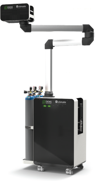
CLIMATE is a plug-and-play system that relies on an innovative micro-electromechanical system (MEMS) device, referred to as the Nano-Reactor, to accurately control the gas environment surrounding the specimen inside the TEM. Together with the Nano-Reactor, the CLIMATE system consists of a functionalized specimen holder, a heating control unit (HCU), a gas supply system (GSS), a vaporizer, and a residual gas analyzer (RGA). The GSS controls the gaseous environment, allowing the user to mix three different gases through mass flow controllers and a mixing valve. The desired gas mixture is then supplied to the sample, where the user can control pressures and flow rates. These parameters can be changed in real time to achieve any gas mixture, at pressures from vacuum to 2000 mbar. The system also offers the capability of controlling the humidity of the gas mixture from 0–100% relative humidity. The HCU provides temperatures from room temperature to 1200°C, which can be maintained with a stability of <0.01°C and settling times of a few seconds. These integrated components are controlled by a single software interface, Impulse. The Nano-Reactor has been designed for stability against mechanical and thermal drift, and the sample may be monitored during experiments at high temperature, high gas pressure, and various gas flows and partial vapor pressures. This patented device (with an on-chip inlet and outlet) results in a unidirectional gas flow over the sample, improving signal/noise ratio and sensitivity of the gas analyzer, in order to detect the gas products from chemical reactions inside the Nano-Reactor. The small size of the microheater allows EDS analysis at temperatures at or above 900°C. The system also allows nano-calorimetry for measuring the amount of thermal energy that is transferred in a chemical reaction and monitoring the endo/exothermic characteristics.
With this system, gas mixture, pressure, flow rate, vapor pressure, temperature, and reaction product analysis can be controlled independently through closed-loop feedback provided by sensors for all variables. Such experimental control is essential for analysis under near operating conditions of battery electrode materials, new catalysts, and new synthesis methods for high-performance materials. Information provided by the CLIMATE system, such as the correlation of particle size/shape, gas composition, atomic and electronic structure, calorimetry, and mass spectroscopy data are important for understanding structure-property relationships and atomic-scale synthesis of novel energy materials.
X-Cite NOVEM Fluorescence Illumination System
Excelitas Technologies Corp.
Developer: Joe Lee

The X-Cite NOVEM is a nine-channel LED illumination system for fluorescence imaging applications. Available configurations cover imaging at shorter wavelengths of the spectrum to the near-IR. The unit has five independent LEDs, outfitted with excitation filters for imaging popular fluorophores such as DAPI, CFP, GFP/FITC, and Cy5. Four additional channels (500–600 nm) are powered by the patented LaserLED Hybrid Drive® technology, with a 4-position motorized filter changer to select specific wavelengths within this range for popular green excited fluorophores such as YFP, TRITC, and mCherry. The preinstalled filters and motorized filter changer make it easy to image with multiband filter cubes without bleed-through. Filters not in use stay in the system so they will not get misplaced in the lab. The X-Cite NOVEM couples to most standard research microscopes with a liquid light guide and an X-Cite microscope adaptor. Each of the nine channels can be controlled individually or combined with others, and rapid channel-switching allows high-throughput imaging. Everyone in the lab will appreciate how quietly the system runs. Even operating at full power, the acoustic noise generated by X-Cite NOVEM is exceptionally low.
For applications such as Fura-2, xenon lamps have long been the light source of choice because of their uniform intensity over a wide range of wavelengths. Fura-2 ratiometric imaging requires equal light intensity at both 340 nm and 380 nm in order to analyze the signal ratio in calcium studies. In an LED system, each of these wavelengths can be controlled separately to capture images at similar excitation intensities. In addition, LED lamps last for tens of thousands of hours, compared to a few hundred hours for xenon lamps. The IR version of the system is able to image in near-IR, using ICG (indocyanine green) and IR800 dyes, providing higher signal-to-noise ratios because of low background autofluorescence in the near-infrared region. Interest in this spectral region (using ICG and IR800) is growing because of its potential use in image-guided surgery. The IR800 dye has high water solubility and stability, low toxicity, and high signal in human tumor cells. Near-IR wavelengths also allow for greater depth penetration in thicker tissues and living animals.
EXpressLO-Z™ FIB/TEM Specimen Grids
EXpressLO LLC
Developers: Lucille Giannuzzi and Nicolaie Moldovan

EXpressLO-Z™ grids consist of conducting nanocrystalline diamond (NCD), which eliminates most overlaps between X-rays emanating from the specimen and from conventional grids. EXpressLO-Z™ grids are produced using lithography and chemical vapor deposition (CVD) methods. Since these grids are made of NCD, they exhibit low inherent X-ray background with a majority carbon K characteristic peak. The 3 mm NCD grids are designed for use in either FIB ex situ lift out (EXLO) or in situ lift out (INLO) specimen preparation. Slots in the grid accept specimens of different lengths, and a half-grid style allows for additional FIB milling (if needed). These grids contain no metals typical of conventional grids (Cu, Mo, Ni, Ta, Au) that produce X-rays that may interfere with X-rays from like elements within the specimen. The CVD deposition yields a smooth grid surface ideal for attaching EXLO or INLO specimens. The NCD grid material can be subjected to high temperatures for in situ heating experiments. The FIB/TEM community has been searching for a low-Z grid material for several years to avoid X-ray peak overlaps. To date, the difficulty has been developing a cost-effective way of manufacturing such grids. Beryllium grids are available but are rarely used because Be is toxic and dangerous to handle. EXpressLO-Z™ grids are carbon-based, stable at high temperatures, and cost-effective.
Avoiding peak overlaps can be important in both qualitative and quantitative X-ray spectrometry. As an example, the use of copper grids must certainly be avoided in the case of a microcircuit with Cu interconnects, high-temperature semiconductor cuprates, or other copper-oxides. The grid material may also emit X-rays that could overlap with X-rays from elements in the specimen. For a Cu grid, likely interferences are between Cu Kα and either Hf Lα or Ta Lα. Similar overlap issues would be observed with Mo, Ni, and other high-Z grids. The high-temperature stability of the grids for specimen heating experiments is also important. It is known that in the absence of oxygen, diamond does not alter its composition up to 1000°C. At that high temperature, the diamond material gradually transforms to graphite, still preserving its carbon-only composition.
Stela™ Hybrid-Pixel Camera
Gatan, Inc.
Developers: Anahita Pakzad, Luca Piazza, Christoph Hoermann, Vittorio Boccone, Paul Mooney, Tom Sha, Mike Petrillo, and Bert Taube

Stela™ is a hybrid-pixel electron detector fully integrated with the Gatan Microscopy Suite (GMS) software for advanced electron diffraction studies. Stela uses the DECTRIS ELA® hybrid-pixel electron detector that employs electron counting to minimize noise and uses on-the-fly digitization. The high dynamic range attained allows the capture of both weak and intense reflections typical of advanced diffraction studies. DECTRIS hybrid-pixel technology provides best-in-class performance in terms of detector noise, frame rate, point spread function, and pixel dynamic range. Stela has been optimized for imaging at low kV, making it ideal for materials that require diffraction studies at <80 kV. At its fast frame rate, the system acquires hardware-synchronized 4D STEM datasets at >16,000 pixels/s. This fast frame rate means the operator can cover a large area of the specimen quickly while reducing specimen drift and damage. Hardware-synchronized 4D STEM eliminates data loss during acquisition. Pre-optimized 4D STEM tools along with Python scripting allow for high-quality data acquisition and processing. Thus, Stela provides visualization and analysis of the 4D data stream, giving the scientist quick and efficient feedback and experimental control.
The 4D STEM is the next big leap for electron microscopy. The combination of both real and reciprocal space in a single dataset opens new opportunities for data analysis, extending real-space resolution to mapping crystallographic changes at near-atomic scale and possibly enabling the development of novel analysis methods. However, there are significant barriers to realizing this potential. A successful 4D STEM experiment relies greatly on robust and easy-to-use software for data acquisition and analysis, and data quality is mainly dictated by the detector used to collect the diffraction patterns. With the introduction of Stela's camera, the DECTRIS high-dynamic-range high-speed hybrid-pixel counting detector is fully integrated into the Gatan Microscopy Suite workflow to enable mainstream adoption of advanced 4D STEM diffraction experiments in electron microscopy labs across the world.
The main application of the Stela camera integrated with DigitalMicrograph is 4D STEM, which allows studies such as strain mapping, orientation mapping, differential phase-contrast imaging, and ptychography. These advanced methods are used in characterization of metals and alloys, ceramics, semiconductors, and 2D materials.
Multi-Model in situ Bulk Liquid-Electrochemistry Microscopy
Hummingbird Scientific
Developers: Norman Salmon and Daan Hein Alsem

Hummingbird Scientific's Multi-model in situ bulk liquid-electrochemistry microscopy platform enables in situ high-magnification microscopy and spectroscopy across TEM, SEM, and X-ray microscopy of liquid-electrochemical processes that match the behavior of bulk electrochemistry. It achieves this while maintaining all the features of traditional in situ liquid cell microscopy systems: nanometer-scale membranes that enclose a thin layer of liquid environment, control of liquid pressure and flow, temperature control from RT to liquid boiling point, electrical biasing, and energy-dispersive X-ray spectrometry (EDS) for elemental analysis. The present innovation involves miniaturizing standard bulk reference and counter electrodes (RE and CE) and placing them in-line with the liquid flow to the specimen. The working electrode (WE) is located on the chip inside the liquid cell for imaging of the electrochemical process of interest. This configuration overcomes issues associated with using quasi-REs and quasi-CEs on-chip, which in previous studies have led to unstable rest potentials and a lack of distinct data peaks. Thus, previous results have been challenging (if not impossible) to relate to the electrochemical process they are supposed to represent. We have overcome these issues with a miniaturized three-electrode bulk liquid-electrochemical cell that is small enough to fit inside the small specimen space in high-magnification TEM, SEM, and X-ray microscopes.
Traditional in situ high-magnification liquid-cell microscopy systems do not incorporate realistic bulk electrodes and reference electrodes. Previous attempts at high-magnification in situ liquid-electrochemical cells employ unreliable on-chip quasi-REs (QREs) inside the liquid cell. Because of the small volume of liquid in the cell, the QRE, which sits in the reagent electrolyte, only provides a quasi-reference potential. As the reagent solution changes during the reaction, so does the reference potential (hence quasi-reference electrode). This makes the chemistry observed unrepresentative of chemistry performed on the beaker scale. The present innovation overcomes this lack of relevance to reaction conditions.
Technologies that could benefit from this liquid-electrochemical system include electrochemical processes related to energy storage devices such as batteries, supercapacitors, and fuel cells. It could also have an impact on nanoscale synthesis for next-generation electronic devices. Thus, the system could aid in the development of lower-cost, longer-lasting, faster-operating, and environmentally friendlier electrical and energy-storage devices.
Helios 5 Laser PFIB
Thermo Fisher Scientific, Inc.
Developers: Marcus Straw, Steven Randolph, Jorge Filevich, Aurelien Botman, Remco Geurts, David Krobot, Tomáš Gancarčik, Ivan Dekan, Václav Šnajdr, and Vit Kloucek

The Helios 5 Laser PFIB enables high-quality subsurface and 3D characterization at millimeter scale with nanometer resolution. It provides large-volume 3D analysis, gallium-free sample preparation, and precise micromachining. With an integrated femtosecond laser, it offers fast material removal rates while maintaining high cut-face quality. The Helios 5 Laser PFIB combines (a) the Elstar SEM column, for ultra-high-resolution imaging and analytical capabilities, (b) a plasma focused ion beam (PFIB) column for high milling performance at all operating conditions, and (c) a femtosecond laser, enabling in situ ablation at unprecedented material removal rates for fast millimeter-scale characterization at nanometer resolution. The ultra-short duration of the femtosecond laser pulses introduces almost no artifacts while delivering higher site-specific accuracy compared to traditional mechanical polishing techniques. The femtosecond laser induces no heat impact, no microcracks, and no melting effects. In most cases, femtosecond laser-milled surfaces are clean enough for direct SEM imaging, and the quality is often sufficient for surface-sensitive electron backscatter diffraction (EBSD) mapping. When it is necessary to further improve the surface quality, a short PFIB polishing procedure can be used to reveal ultra-fine features. Compared to a Ga FIB, the plasma-based FIB optimally complements the femtosecond laser to maintain a high throughput. All three beams (SEM/FIB/laser) point at a single point, enabling short laser/SEM switching times and no vacuum transfers. Automated, ultra-large-volume 3D characterization using laser tomography is a particular capability.
The femtosecond laser can cut materials orders of magnitude faster than a Ga FIB. For many materials, a large cross section hundreds of micrometers wide can be created within 5 minutes. By using a different removal mechanism, ablation versus ion sputtering, the laser can process challenging materials such as non-conductive or ion-beam-sensitive samples: glass, ceramics, hard and soft polymers, biomaterials, and graphite. A protective coating to reduce charging or to mitigate the curtain artifacts is not needed, saving time and increasing throughput.
This Laser PFIB enables new applications such as large-volume cross-sectioning for rapid failure analysis; fast access to buried subsurface layers; fast micromachining of complex shapes such as tensile rods, chunks, and microCT specimens; and millimeter-scale 3D laser serial sectioning, including analytical characterization with EDS X-ray spectrometry or EBSD.
alpha300 apyron Automated Raman Microscope
WITec GmbH
Developers: Olaf Hollricher, Wolfram Ibach, Peter Spizig, Christian Weberbauer, Detlef Sanchen, and Christian Hermann

The WITec alpha300 apyron is an advanced, fully automated, confocal Raman microscope. It uses motorized optical components to provide the benefits of high-resolution 3D chemical characterization in a matter of minutes to researchers of all experience levels. The alpha300 apyron broke new ground by introducing self-alignment, self-calibration, and remote operation. Opto-mechanical modules that enable automated optimization include a calibration source that can validate and calibrate spectrometer gratings, an output coupler that maximizes signal throughput to a spectrometer, and motorized iris diaphragms that adjust the beam path for optimum contrast and homogeneity in white-light imaging. The alpha300 apyron increases sample throughput rate by optimizing performance for every experimental setup. Software-driven routines ensure the consistency and reproducibility of results while also substantially reducing the researcher's workload by requiring less user input and eliminating potential sources of error. The alpha300 apyron can configure the beam path to perform measurements with methods complementary to Raman microscopy while the sample remains at the same position.
It allows excitation laser wavelengths to be chosen to best produce the Raman effect, or to generate or avoid photoluminescence from the sample. It also features multi-laser input coupler technology that can adjust the optical elements for each wavelength. All these features are accessible through the WITec Suite FIVE control software and EasyLink handheld controller. Only the mounting of the sample on the microscope stage requires physical interaction, which enables remote operation while the instrument is in an environmental enclosure or at a location separate from the researcher. Advanced Raman imaging experiments often include many optical elements in beam paths. New functionalities include polarization-dependent measurements with motorized polarizer and analyzer rotation, push-button spectrometer connection and signal maximization, and automated adjustment of both iris diaphragms. Standardized optical modules in an integrated software environment allow new capabilities.
Raman microscopy, long used by specialists in purely scientific research, is being employed as a routine analysis tool in an ever-growing range of fields, and automation makes the technique easier to use. The alpha300 apyron's optimized performance will benefit scientists working in materials science, environmental science and microparticle analysis, life science, food science, geology, pharmaceutics, and many other fields.
