


Introduction
The overgrowing need for electrical and electronic devices in the current era has escalated the inevitable threat of electromagnetic (EM) pollution in our environment. Hence, the development of devices that can plunge EM pollution is in great demand. One such device capable of mitigating EM pollution is an EM absorber. It plays a vital role in diverse applications in the commercial and military spheres [Reference Tirkey and Gupta1–Reference Vinoy and Jha4].
The EM absorbers have a very long history since the 1930s. The research effort for absorbers intensified, especially after the introduction of microwave radar during World War II [Reference Vinoy and Jha4]. A large variety of absorbing devices have been designed, studied, and constructed. The classical resonant absorbers, such as the Salisbury screen and the Dallenbach absorber, offer perfect absorption at their resonant frequency but are limited by narrow bandwidth and quarter-wavelength thickness [Reference Tirkey and Gupta1].
The classical broadband absorbers, such as multilayered Salisbury screen (Jaumann absorber) and multilayered Dallenbach absorber, offer a broadband reflection reduction of −15 to −20 dB near normal incidence. This multilayer approach increases the overall thickness of the absorber at multiples of quarter-wavelength [Reference Vinoy and Jha4, Reference Emerson5]. Consequently, these devices have limited practical applications due to their thick and bulky structural design.
The metamaterial, metasurface, and frequency selective surface (FSS) based absorbers that emerged in the last decade can provide near-perfect absorption through a thin profile [Reference Zhang, Jiang, Wang, Zhao, Wang, Du, Wang and Huang6–Reference Xiong, Chen, Cheng and Luo12]. However, the bandwidth of these devices is inherently narrow [Reference Tirkey and Gupta1, Reference Tirkey and Gupta3]. The circuit analog absorbers provide enlarged absorption bandwidth at a thinner configuration [Reference Yu, Besteiro, Huang, Wu, Fu, Tan, Jagadish, Wiederrecht, Govorov and Wang2].
The design of broadband absorbers has been extensively studied [Reference Xiong, Chen, Cheng and Luo12–Reference Lim, Yu and Lim23]. However, these absorbers consider the conventional −10 dB level for representing their absorption bandwidth. Only a few articles are available considering the −20 dB level to represent broadband absorption bandwidth [Reference Tang, Goussetis, Legay and Fonseca18–Reference Sohrab and Atlasbaf20]. It is worth mentioning that a −10 dB bandwidth corresponds to only 90% absorption of incident waves, and the remaining 10% is reflected. Similarly, −20 dB bandwidth indicates that 99% of incident waves are absorbed, while the remaining 1% is still not absorbed. The pyramidal absorbers, primarily used for constructing the anechoic chambers, consider lower than −40 dB reflection level for maintaining an excellent absorptivity level over a broad frequency band [Reference Emerson5]. However, they find limited applications because of their thick, bulky, and fragile structure.
A comprehensive literature survey [Reference Tirkey and Gupta1–Reference Tirkey and Gupta3] manifests that most of the absorbers showing excellent absorption performance are thick and bulky, while a thin and low-profile absorber possesses limited bandwidth. This is due to the inverse relationship between bandwidth and thickness [Reference Rozanov24]. A trade-off between bandwidth and thickness generally results in a low absorptivity level. Hence, a −10 dB bandwidth is used to represent the 90% absorptivity level in most cases. The absorber design becomes even more challenging when the constraints such as broad bandwidth, low thickness, and high absorptivity level are required to be satisfied simultaneously. The ultimate goal is to design a thin broadband absorber that exhibits near-unity absorption throughout the absorption band.
In this letter, an attempt has been made to achieve perfect broadband absorption through a thin planar absorber for microwave applications. This is different from what we usually observe; nevertheless, this is one of the most anticipated problems that the researchers of this specific domain have been trying to solve since the first experimental demonstration of a perfect metamaterial absorber in 2008 [Reference Landy, Sajuyigbe, Mock, Smith and Padilla25].
Here, we have successfully solved a highly challenging problem of achieving near-unity absorption throughout a broad frequency range with a thin absorber. To be precise, we have achieved 99.99% absorbance by lowering the reflection coefficient to less than −40 dB at normal incidence while keeping the transmission coefficient zero using an entirely conducting ground plane. By ensuring that the incident radiations are efficiently dissipated in the form of proper losses exhibited by the absorber, a fractional bandwidth of 19.03% is achieved at 99.99% absorbance. Moreover, the absorber is thin (0.22λ 0 at the center frequency) and polarization-insensitive.
Theory and conditions
Let us consider an incident plane wave with the electric and magnetic fields E $_\mathrm{inc}$ and H
 $_\mathrm{inc}$, respectively, which are uniform in the plane of the infinite periodic array of the absorber.
The absorptivity (A) of an EM absorber is related to the reflection (S $_\mathbf{11}$) and transmission (S
 $_\mathbf{21}$) coefficients as follows [Reference Landy, Sajuyigbe, Mock, Smith and Padilla25, Reference Tirkey and Gupta26]:
 \begin{equation}
\mathbf{A}=1-\left|\mathbf{S}_{\mathbf{1 1}}\right|^{2}-\left|\mathbf{S}_{\mathbf{2 1}}\right|^{2}.
\end{equation}
\begin{equation}
\mathbf{A}=1-\left|\mathbf{S}_{\mathbf{1 1}}\right|^{2}-\left|\mathbf{S}_{\mathbf{2 1}}\right|^{2}.
\end{equation}Following are the experimental conditions that ensure the −40 dB absorption of arbitrarily polarized normally incident plane waves through an absorber, provided the absorber incorporates adequate losses to dissipate the entire incident waves.
 \begin{equation}
\mathbf{A} \gt 0.9999,
\end{equation}
\begin{equation}
\mathbf{A} \gt 0.9999,
\end{equation} \begin{equation}\text{Reflected Fields:}\ {\mathbf E}_{\mathrm r}\approx0,{\mathbf H}_{\mathrm r}\approx0,\end{equation}
 \begin{equation}
\begin{array}{ll}
\left|\mathbf{S}_{\mathbf{1 1}_\mathrm{TE}}^{\mathrm{co}}\right|^{2} \lt 1 \textrm{E-4}, & \left|\mathbf{S}_{\mathbf{1 1}_{\mathrm{TE}}}^{\mathrm{cr}}\right|^{2} \lt 1 \textrm{E-7}, \\
\left|\mathbf{S}_{\mathbf{1 1}_{\mathrm{TM}}}^{\mathrm{co}}\right|^{2} \lt 1 \textrm{E-4}, & \left|\mathbf{S}_{\mathbf{1 1}_\mathrm{TM}}^{\mathrm{cr}}\right|^{2} \lt 1 \textrm{E-7},
\end{array}
\end{equation}
\begin{equation}
\begin{array}{ll}
\left|\mathbf{S}_{\mathbf{1 1}_\mathrm{TE}}^{\mathrm{co}}\right|^{2} \lt 1 \textrm{E-4}, & \left|\mathbf{S}_{\mathbf{1 1}_{\mathrm{TE}}}^{\mathrm{cr}}\right|^{2} \lt 1 \textrm{E-7}, \\
\left|\mathbf{S}_{\mathbf{1 1}_{\mathrm{TM}}}^{\mathrm{co}}\right|^{2} \lt 1 \textrm{E-4}, & \left|\mathbf{S}_{\mathbf{1 1}_\mathrm{TM}}^{\mathrm{cr}}\right|^{2} \lt 1 \textrm{E-7},
\end{array}
\end{equation} \begin{equation}\text{Transmitted Fields:}\ {\mathbf E}_{\mathrm t}=0,{\mathbf H}_{\mathrm t}=0,\end{equation}
 \begin{equation}
\begin{array}{ll}
\left|\mathbf{S}_{\mathbf{2 1}_\mathrm{TE}}^{\mathrm{co}}\right|^{2}=0, & \left|\mathbf{S}_{\mathbf{2 1}_{\mathrm{TE}}}^{\mathrm{cr}}\right|^{2}=0,\\
\left|\mathbf{S}_{\mathbf{2 1}_{\mathrm{TM}}}^{\mathrm{co}}\right|^{2}=0, & \left|\mathbf{S}_{\mathbf{2 1}_\mathrm{TM}}^{\mathrm{cr}}\right|^{2}=0.
\end{array}
\end{equation}
\begin{equation}
\begin{array}{ll}
\left|\mathbf{S}_{\mathbf{2 1}_\mathrm{TE}}^{\mathrm{co}}\right|^{2}=0, & \left|\mathbf{S}_{\mathbf{2 1}_{\mathrm{TE}}}^{\mathrm{cr}}\right|^{2}=0,\\
\left|\mathbf{S}_{\mathbf{2 1}_{\mathrm{TM}}}^{\mathrm{co}}\right|^{2}=0, & \left|\mathbf{S}_{\mathbf{2 1}_\mathrm{TM}}^{\mathrm{cr}}\right|^{2}=0.
\end{array}
\end{equation}Here, the indices “co” and “cr” represent the co- and cross-polarized components.
Design and configuration
We present the design of a simple star-shaped FSS (SFSS) structure in Fig. 1. The SFSS is chosen and designed to couple both the electric and magnetic fields simultaneously. We propose this planar SFSS in the form of a resistive layer, with a sheet resistance of 101  $\Omega/$sq, to achieve near unity absorption throughout a wide passband.

Figure 1. Schematic of the proposed absorber: (a) periodic array depicting the scenario of perfect absorption at microwave realm, (b) side view showing the layer configuration, and (c) top view of the unit cell. Dimensions: a = 4.762, b = 8.019, c = 3.742, d = 0.423, s = 19,  $h1 = 0.177$, and
  $h2 = 6.2$ (unit: mm).
The absorber consists of a single layer of an infinite periodic array of the SFSS unit cell deposited on a thin paper substrate ( $\varepsilon_{\mathrm r}=2.5$,
  $\tan\delta=0.05$). The lattice of the unit cell is kept more petite than the operating wavelength to avoid the generation of grating lobes. This printed layer is placed above a conducting ground plane separated by a lossless foam interlayer. The thickness of this interlayer is kept smaller than the quarter wavelength to make the absorber thin and lightweight.
The impedance of the absorber is perfectly matched to the free space impedance over a broad passband by optimizing the thickness of the foam layer and the geometry of the SFSS. The SFSS structure exhibits a complex reactive property and provides high ohmic losses due to its resistive profile. A properly optimized reactive and resistive properties of the SFSS allow the absorber to dissipate the entire incident waves in a wide passband.
Full wave simulation
A full wave simulation is carried out to analyze the characteristics of the proposed absorber. A brief outline of the simulation procedure is given below.
Simulator
High frequency structure simulator (HFSS)
Solver
Finite element method
Simulation procedure
We first designed a single unit cell of the proposed absorber. Then we applied proper boundary conditions to simulate an infinite periodic array of the designed unit cell. The applied boundaries were two master–slave pairs. We added a pair of Floquet ports as the excitations to excite the incident EM wave upon the top surface of the unit cell. We defined the polarization and incidence angles as “phi” and “theta” on the Floquet ports. We created a free-space environment for the simulation with these master–slave boundaries and Floquet port excitations. After that, we added an analysis setup and simulated the designed unit cell of the proposed structure. After simulation, we plotted the S-parameters and calculated the absorptivity using Equation (1). Then we analyzed the results and optimized the design to achieve the desired characteristics.
Absorption characteristics
The reflection coefficients of the absorber simulated under normal incidence are plotted in Fig. 2. The transmission coefficient is zero due to the conducting ground plane. We have achieved the following characteristics illustrated in Figs. 2, 3, and 4, ensuring perfect absorption conditions.
• The co-reflection coefficient is below −40 dB from 9.7 to 11.74 GHz (Fig. 2).
• The cross-reflection coefficient is below −70 dB in the entire working band (Fig. 2).
• The reflection characteristics are identical for both the TE and TM modes (Fig. 2).
• The absorptivity curve shows near-unity absorptivity throughout a broad bandwidth (Fig. 3).
• The absorptivity value is more than 0.9999 from 9.7 to 11.74 GHz (Fig. 3).
• The reflection characteristics are identical for all arbitrarily polarized incident plane waves (Fig. 4).

Figure 2. Simulated reflection coefficients illustrating −40 dB and −70 dB, co- and cross-reflection reductions to absorb 99.99% incident plane waves.

Figure 3. Absorptivity curve of the proposed absorber showing broadband absorption above 0.9999 from 9.7 to 11.74 GHz.

Figure 4. Reflection coefficient at different polarization angles  $(\phi)$ demonstrating identical characteristics for all arbitrary polarization of incident waves.
The above observations confirm that the proposed absorber provides a near unity absorption from 9.7 to 11.74 GHz. The absorber maintains an excellent impedance matching throughout the working band and sustains a negligible reflection value (below 0.0001). The absorber is polarization-insensitive due to the fourfold symmetric structure of the SFSS. The absorber performance at different values of reflectivity level is summarized in Table 1.
Table 1. Absorber performance at different reflectivity levels

* FBW = fractional bandwidth = bandwidth/center frequency (10.72 GHz)
Optimum thickness ratio
We determine the optimum thickness ratio (OTR) to estimate the ultimate performance of the proposed absorber by comparing its performance with an optimum design characterized by similar characteristics.
K. N. Rozanov developed an inequality (7) that relates the total thickness of a metal-backed absorber with bandwidth at a given reflection coefficient to estimate its optimum thickness [Reference Rozanov24].
 \begin{equation}
\left|\int_{0}^{\infty} \ln |\rho(\lambda)|\,\mathrm{d} \lambda \right| \leq 2 \pi^{2} \sum_{i} \mu_{\mathrm{s}, {i}} {d}_{i},
\end{equation}
\begin{equation}
\left|\int_{0}^{\infty} \ln |\rho(\lambda)|\,\mathrm{d} \lambda \right| \leq 2 \pi^{2} \sum_{i} \mu_{\mathrm{s}, {i}} {d}_{i},
\end{equation}where  $\mu_{\mathrm{s}, {i}}$ and
  ${d}_{i}$ are the static permeability and thickness of the absorber’s i th layer. Since a broadband absorber offers a finite bandwidth, its reflection coefficient is related as follows:
 \begin{equation}
\ln |\rho(\lambda)|=\left\{\begin{aligned}
\hspace{1mm} {k}|\Gamma(\lambda)|, & \hspace{6mm} \lambda_{\min } \leq \lambda \leq \lambda_{\max } \\
\hspace{1mm} 0, & \hspace{6mm} \text {otherwise }
\end{aligned}
\right.
\end{equation}
\begin{equation}
\ln |\rho(\lambda)|=\left\{\begin{aligned}
\hspace{1mm} {k}|\Gamma(\lambda)|, & \hspace{6mm} \lambda_{\min } \leq \lambda \leq \lambda_{\max } \\
\hspace{1mm} 0, & \hspace{6mm} \text {otherwise }
\end{aligned}
\right.
\end{equation}where  $\Gamma(\lambda)=20\, \log |\rho(\lambda)|$ and
  ${k}= (\ln 10)/20$, and for nonmagnetic absorbers
  $\mu_{\mathrm{s}, {i}} \equiv 1$. Hence, the optimum thickness
  $(T_{\mathrm O\mathrm T})$ of the absorber can be expressed as
 \begin{equation}
{T}_{\mathrm{OT}} \geq \frac{{k}}{2 \pi^{2}}\left|\int_{\lambda_{\min }}^{\lambda_{\max }}| \Gamma(\lambda)|\,\mathrm{d} \lambda\right|
\end{equation}
\begin{equation}
{T}_{\mathrm{OT}} \geq \frac{{k}}{2 \pi^{2}}\left|\int_{\lambda_{\min }}^{\lambda_{\max }}| \Gamma(\lambda)|\,\mathrm{d} \lambda\right|
\end{equation} For an optimum absorber, inequality (9) states that  ${k}/2 \pi^{2}$ times the area of the reflection spectra over the whole waveband should not exceed an optimum thickness. It provides the minimum achievable thickness for a physically realizable nonmagnetic broadband absorber.
The integral in Equation (9) is determined by considering the entire frequency range, i.e., 2–20 GHz (not the −10 dB frequency range). Then the complete reflection coefficient plot of the absorber is mapped in the wavelength domain and quantized with a step size of 0.5 dB from 0 to −40 dB to obtain a smooth estimation of this curve from  $\lambda_{\min}$=15 mm to
  $\lambda_{\max}$=150 mm. Finally, the optimum thickness of the proposed design is estimated to be 5.4 mm. The real thickness of the absorber (6.377 mm) is close to this optimum thickness limit.
The OTR is defined as the ratio of the optimum thickness  $({T}_\mathrm{OT})$ to the real thickness
  $({T}_\mathrm{RT})$ of the absorber [Reference Beeharry, Yahiaoui, Selemani and Ouslimani16].
 \begin{equation}
\mathrm{OTR}=\frac{{T}_{\mathrm{OT}}}{{T}_{\mathrm{RT}}} \times 100
\end{equation}
\begin{equation}
\mathrm{OTR}=\frac{{T}_{\mathrm{OT}}}{{T}_{\mathrm{RT}}} \times 100
\end{equation}Equation (10) describes that when the optimum and the real thicknesses are equal, it results in a 100% OTR. A higher value of OTR means the real thickness of the absorber is closer to its optimum thickness limit. The OTR of the proposed absorber is calculated as high as 84.68%, demonstrating a good performance compared to the optimum design. The OTR of the proposed absorber is also compared with some other broadband absorbers in Table 2. It is evident that the proposed absorber outperforms the other absorbers in terms of OTR.
Table 2. OTR comparison of the proposed absorber with some other broadband absorbers

* The entire frequency range in which the reflection coefficients were investigated is considered here, not the −10 dB frequency range.
Absorption mechanism
The geometry of the SFSS unit cell is a highly symmetrical element. When plane waves are normally incident on this symmetrical element, an electric dipole moment P is induced by the incident electric field. Similarly, the incident magnetic field produces a magnetic moment M so that both moments are orthogonal to each other. The electric field distribution and electric current density of the unit cell at the center frequency (10.72 GHz) depicted in Figs. 5 and 6, respectively, explain the generation of both moments.

Figure 5. (a) Magnitude and (b) vector distributions of electric field at 10.72 GHz, illustrating the electric dipole formation between two neighboring unit cells.

Figure 6. (a) Surface current distribution at 10.72 GHz, (b) illustration of magnetic field generation due to the counterclockwise (CCW) and clockwise (CW) current loops, and (c) magnetic field distribution at 10.72 GHz.
In Fig. 5, it is demonstrated that the coupling between neighboring unit cells results in the separation of the positive and negative charges in the right and left edges of the unit cell due to the y-polarized incident electric field. This charge separation results in the formation of an electric dipole moment P between two neighboring unit cells.
Figure 6 illustrates that circulating surface current loops are generated in the right and left portions of the SFSS in the counterclockwise and clockwise directions, respectively. This closed circulation of the electric current system produces a magnetic dipole moment M. The resulting magnetic field emerges out of the right counterclockwise loop and goes down to the left clockwise loop when the incident electric field is directed along the y-axis.
The electric and magnetic dipole moments created by the infinite periodic array of the SFSS unit element generate secondary plane waves. When both moments are appropriately tuned, they cancel the incident plane waves. Hence, the proposed absorber efficiently absorbs the electric and magnetic fields of the incident wave.
Parametric study
The parametric study of the geometrical parameters of the SFSS is carried out to demonstrate its impact on the performance of the absorber. The two main geometrical parameters of the star shape of the FSS, viz. “a” and “b,” are investigated initially.
The absorber’s response for different values of the parameter “a” is plotted in Fig. 7. When the value of “a” is gradually increased from 4.76 to 4.96 mm, it is observed that the lower resonance decreases and the reflection spectrum shifts to a lower value. However, the upper resonance does not deviate at the cost of an increased reflection coefficient. As a result, the bandwidth is widened, but the reflection level increases from −40 dB to around −25 dB. The best result with −40 dB bandwidth is obtained at a = 4.76 mm.

Figure 7. Simulated reflection coefficient for different values of the geometric parameter “a” of the SFSS (Unit: mm).
Next, the value of “b” is varied from 7.8 to 8.6 mm, and the reflection spectra of the absorber are plotted in Fig. 8. It illustrates that the lower and upper resonant frequencies of the absorber can be controlled by varying the geometric parameter “b.” The lower resonant frequency is controlled by reducing the value of “b” below 8 mm, and the upper resonant frequency is controlled by raising its value above 8 mm. Hence, b = 8 mm is a good trade-off value, which results in a balanced reflection coefficient at both resonant frequencies and provides a wide bandwidth below −40 dB level.

Figure 8. Simulated reflection coefficient for different values of the geometric parameter “b” of the SFSS (Unit: mm).
It should be noted that the variation in the values of “a” and “b” affect the geometrical parameters “c” and “d” of the SFSS. The parameters “c” and “d” both increase by increasing the value of “b.” However, “d” reduces with the increase in “a”. Hence, a separate study of “c” and “d” is not presented here as their effect can be ascertained from the parametric study of “a” and “b.”
Further, the parametric variation of the periodicity “s” is investigated, and the resulting reflection spectra are plotted in Fig. 9. It demonstrates that periodicity plays a significant role in matching the impedance of the absorber to the impedance of the free space. When the value of “s” gradually increases from 16 to 19 mm, the lower resonant frequency shifts to a higher frequency range and comes closer to the upper resonant frequency. As a result, the reflection level decreases from −10 to −40 dB. It indicates that the absorber’s impedance comes closer to the free space impedance. Hence, the reflection level of the absorber’s passband can be controlled by modifying the periodicity of the structure.

Figure 9. Simulated reflection coefficient for different values of the periodicity “s” of the unit cell (Unit: mm).
The SFSS structure is also investigated for different values of scaling factor. As demonstrated in Fig. 10, a slight change in the scaling factor “X” results in an abrupt change in the response of the absorber. When the scaling factor “X” gradually increases from 1 to 1.15, the reflection level increases from −40 to −10 dB. It explains that the reflection level can also be customized by scaling the size of the unit cell pattern. The geometrical parameters corresponding to X = 1 provide the best response, as shown in Fig. 10.

Figure 10. Simulated reflection coefficient for different values of the scaling factor “X” of the SFSS pattern.
Next, the effect of the sheet resistance of the SFSS layer is investigated and reported in Fig. 11. When the sheet resistance is varied from 80 to 101  $\Omega/$sq, the upper and lower resonant frequencies move toward each other. The mid-band of the curve also goes down with the increase in the sheet resistance. It explains that the sheet resistance directly affects the impedance matching of the absorber. Hence, a −40 dB reflection level is achieved by ensuring proper sheet resistance of the SFSS layer (in this case, 101
  $\Omega/$sq).

Figure 11. Simulated reflection coefficient for different values of the sheet resistance of the top SFSS pattern (Unit: Ω/sq).
Finally, the height of the foam layer ( $h2$) is varied from 6 to 6.5 mm to show its impact on the reflection curve of the absorber. Figure 12 demonstrates that the height of the foam layer has a direct effect on the resonant frequency of the absorber. Lower values of “
 $h2$” excite the lower resonant frequency, while its higher values excite the upper resonant frequency. It is also observed that when the reflection coefficient at the lower resonant frequency reduces, the reflection coefficient at the upper resonant frequency increases and vice versa. It explains the inverse relationship between the height and the bandwidth of the absorber. Hence, a trade-off is taken to render a balanced performance of the absorber. The reflection coefficient of the curve shows a balanced response when
  ${h2}=6.2$ mm.

Figure 12. Simulated reflection coefficient for different values of the height “ $h2$” of the foam substrate (Unit: mm).
This extensive parametric study explains that the −40 dB reflection level can be achieved by ensuring a proper balance between all the optimized geometrical parameters of the unit cell pattern, its sheet resistance, and the separation between the top printed layer and the ground plane of the absorber.
Equivalent circuit model
A transmission line-based equivalent circuit model of the proposed absorber is developed for normally incident plane waves and presented in Fig. 13. It consists of a series combination of a resistor, an inductor, and a capacitor forming an RLC circuit. Additionally, a capacitor in parallel connection with this RLC circuit terminated by ground is also present. The expression of the impedance of the top FSS array is given as

Figure 13. Transmission line equivalent circuit model of the proposed absorber under normal incidence.
 \begin{equation}
{Z}_{\mathrm{FSS}}={R}_{1}+\left[\left({R}_{2}+{j} \omega {L}_{1}+\frac{1}{{j} \omega {C}_{1}}\right) \| \frac{1}{{j} \omega {C}_{2}}\right].
\end{equation}
\begin{equation}
{Z}_{\mathrm{FSS}}={R}_{1}+\left[\left({R}_{2}+{j} \omega {L}_{1}+\frac{1}{{j} \omega {C}_{1}}\right) \| \frac{1}{{j} \omega {C}_{2}}\right].
\end{equation}The FSS layer exerts high ohmic losses in the structure due to the current flowing through the highly resistive patterns. R 1 and R 2 denote the equivalent resistances due to the vertices and the middle portion of the star-shaped structure.
The FSS pattern also exhibits inductive and capacitive effects on the geometry due to the flow of circulating current loops on the structure. L 1 and C 2 signify the equivalent inductance and capacitance representing this inductive and capacitive effect. C 1 expresses the inter-unit cell capacitance originating due to the strong coupling between the neighboring unit cells.
The absorber consists of paper and foam substrates. These are represented as two cascaded transmission line segments in the equivalent circuit, where TL1 and TL2 denote the paper and foam substrates.
A parallel combination of the impedance of the top FSS layer  $({Z_{\mathrm {FSS}}})$ with these two cascaded transmission line segments terminated by a short circuit constitutes the overall input impedance
  $({Z_{\mathrm {IN}}})$ of the absorber. The circuit is shorted to model the ground plane placed below the foam substrate. The expression of the complex input impedance
  ${Z_{\mathrm {IN}}}$ is given as follows:
 \begin{equation}
{Z}_{\mathrm{IN}}={Z}_{\mathrm{FSS}}\| {Z}_{\mathrm{D} 1},
\end{equation}
\begin{equation}
{Z}_{\mathrm{IN}}={Z}_{\mathrm{FSS}}\| {Z}_{\mathrm{D} 1},
\end{equation} \begin{equation}
{Z}_{\mathrm{D} 1}={Z}_{01} \frac{{Z}_{\mathrm{D} 2}+{j} {Z}_{01}\, \tan\left(\beta_{1} {h}_{1}\right)}{{Z}_{01}+{j} {Z}_{\mathrm{D} 2}\, \tan\left(\beta_{1} {h}_{1}\right)},
\end{equation}
\begin{equation}
{Z}_{\mathrm{D} 1}={Z}_{01} \frac{{Z}_{\mathrm{D} 2}+{j} {Z}_{01}\, \tan\left(\beta_{1} {h}_{1}\right)}{{Z}_{01}+{j} {Z}_{\mathrm{D} 2}\, \tan\left(\beta_{1} {h}_{1}\right)},
\end{equation} \begin{equation}
{Z}_{\mathrm{D} 2}={jZ}_{02} \,\tan\left(\beta_{2} {h}_{2}\right),
\end{equation}
\begin{equation}
{Z}_{\mathrm{D} 2}={jZ}_{02} \,\tan\left(\beta_{2} {h}_{2}\right),
\end{equation} ${Z}_{0 {i}}=\frac{{Z}_{0}}{\sqrt{\varepsilon_{\mathrm{r}i}}}$ and
 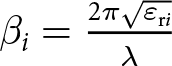 $\beta_{{i}}=\frac{2 \pi \sqrt{\varepsilon_{\mathrm{r}i}}}{\lambda}$ are the intrinsic impedances and phase constants of the ith transmission line section (i = 1, 2).
  ${Z}_{\mathrm{D} 2}$ is an imaginary impedance resulting from the grounded transmission line TL2.
  ${Z}_{\mathrm{D} 1}$ is a complex impedance resulting from the shunt combination of TL1 and grounded TL2.
The equivalent circuit of the absorber is verified by simulating the circuit model in Keysight’s Advanced Design System (ADS) simulation tool. The lumped circuit parameters of the circuit model are obtained by using the curve fitting technique in the ADS simulator. The reflection coefficient can be reduced below −40 dB level by optimizing the circuit parameters to maintain its input impedance close to the free space impedance within the target bandwidth.
The optimized values of the parameters are estimated as  $R_1=109~\Omega$,
  $R_2=265~\Omega$,
  $L_1=2.8$ nH,
  $C_1=75$ fF, and
  $C_2=2.4$ fF. The reflection co-efficient plots obtained from the equivalent circuit simulation using ADS and the full-wave simulation using HFSS are compared in Fig. 14. The comparison confirms a good agreement between both results.

Figure 14. Comparison of the proposed absorber’s reflection coefficient obtained through full-wave simulation using HFSS and equivalent circuit simulation using ADS.
Fabrication and experimental demonstration
The −40 dB broadband absorption claimed in the previous sections is experimentally demonstrated in this section by fabricating a sample prototype of the proposed absorber, as shown in Fig. 15. The fabrication procedure is illustrated below.

Figure 15. (a) Monostatic RCS measurement setup and (b) fabricated prototype of the proposed absorber.
To fabricate the proposed structure, we have used paper and foam materials as the substrates, an inkjet printer, and silver nanoparticle ink as the inkjet material. A periodic array consisting of  $10\times10$ SFSS unit cells is printed on a thin paper substrate. A low-cost inkjet printing technique is adopted for printing the periodic array. The patterns are printed by incorporating silver nanoparticle ink in the inkjet printer. This printed layer is then placed over a foam substrate. Finally, a copper foil is applied at the bottom of the foam substrate to form a ground layer.
The surface resistance value is controlled by digitally controlling the dot density of the ink. The red, green, and blue (RGB) color codes were varied between (0, 0, 0) and (50, 50, 50) to produce a range of different dot densities. In this fabrication process, this setting and the silver ink concentration can be adjusted to precisely obtain the surface resistance value required for the optimum design of the absorber. The detailed procedure is given in [Reference Zabri, Cahill, Conway and Schuchinsky27].
The fabricated prototype has a total area of  $190\times190$ mm2. The paper and foam substrates are
  $0.177\pm0.02$ and 6.2 mm thick, making the final prototype
  $6.377\pm0.02$ mm thick.
The performance of the fabricated prototype is measured by devising a standard far-field monostatic RCS measurement setup in free space for normal incidence, as shown in Fig. 15. The setup includes an Agilant (N5230A) PNA series vector network analyzer, a standard-gain horn antenna, and an anechoic chamber. A detailed description of this standard measurement procedure is provided in [Reference Lim, Yu and Lim23]. The difference is that we have placed the sample prototype at the center of a small anechoic chamber to prevent any unwanted reflected and scattered waves. A single horn antenna is employed at an equivalent height as the sample prototype for measuring the reflection coefficient under normal incidence. The horn antenna is situated 1 m from the sample to satisfy the far-field condition. The noise floor of the hollow anechoic chamber without any sample is measured. The recorded noise floor level is pretty low and remains below −80 dB within the entire working band, as shown in Fig. 16.

Figure 16. Measured reflection coefficient curves of the background noise, reference metal, and the proposed −40 dB absorber.
The measurement is carried out through proper calibration of the setup to reduce the measurement errors. For calibration purposes, a metal plate with an identical dimension to that of the fabricated prototype is placed at the center of the chamber. Then the reflection co-efficient of this metal plate is measured and used as a reference level. Then the fabricated prototype is situated at the center of the chamber after removing the copper plate. The reflection coefficient of the prototype is measured and normalized, with the reference level measured earlier to yield the actual response of the sample prototype.
The sample prototype is expected to provide a −40 dB passband, which requires high accuracy of both the sample and the measurement result. Hence, multiple attempts of fabrication and measurement have been carried out to reach the expected results with minimal discrepancy. The measured reflection coefficient curves of the background noise, reference metal, and the proposed 40 dB absorber are plotted in Fig. 16. The measured result of the proposed absorber is compared with the simulated results after achieving a good agreement among them. As evident from Fig. 17, the measured −40 dB absorption band of the fabricated prototype covers the expected 9.7–11.74 GHz range. Hence, we have successfully demonstrated the −40 dB perfect broadband absorption experimentally. A little discrepancy between the simulation and the measurement results may be attributed to the fabrication tolerances and the measurement errors.

Figure 17. Comparison of the simulated and measured reflection coefficients of the proposed absorber.
Performance comparison
To the best of our knowledge, a polarization-insensitive FSS-based absorber with a reflection level of −40 dB over a broad range of frequencies is not reported in the literature. Hence, we have considered some earlier reported broadband absorbers offering a reflection level lower than the conventional −10 dB level for the performance comparison of our absorber with them in Table 3. We have included the absorber details with −20, −30, and −40 dB reflection levels for a fair comparison between the compared absorbers. The operating frequency range of all the absorbers compared here operate at the X-band range. The comparison is carried out between the fractional bandwidth, thickness, polarization insensitivity, and the total number of layers at a given reflection level to examine the superiority of the proposed absorber.
Table 3. Performance comparison of the proposed absorber with some existing broadband absorbers having a reflection level lower than the conventional −10 dB level

* Total layer considers all the conductive, resistive, and dielectric layers including the ground plane. λ 0 = wavelength corresponding to the center operating frequency, PI = polarization-insensitive, NI = not investigated.
While the prime focus of the proposed work is to achieve the −40 dB broadband absorption, it also depicts several remarkable characteristics. It is a low-cost and efficient absorber that offers a balanced performance in terms of reflection level, bandwidth, thickness, polarization insensitivity, complexity, and ease of fabrication. The thickness of the resulting absorber is already shown to be close to its optimum thickness limit. The low-cost inkjet printing technique used here provides an easy fabrication of the structure. Moreover, the paper and foam materials used in this work are economical and commercially available. It is evident from Table 3 that the proposed absorber provides a good balance among the characteristic parameters with a better performance.
Conclusion
We have presented a thin microwave absorber depicting perfect broadband absorption. An extremely deep reflection coefficient characteristic reaching a level of less than −40 dB is achieved. The absorber provides more than 99.99% absorption of arbitrarily polarized normally incident plane waves from 9.7 to 11.74 GHz. The most important conclusion drawn from this work is that a proper selection and balance of the geometrical parameters, resistive property, along with an optimal thickness of the foam interlayer can offer excellent impedance matching and result in the perfect broadband absorption.
Funding statement
This research received no specific grant from any funding agency, commercial, or not-for-profit sectors.
Competing interests
The authors report no conflict of interest.


