


Introduction
The growth of GaN is challenging, in part due to the independent optimisation of many growth parameters, and also due to the constraint of heteroepitaxy. Typically, sapphire or SiC substrates are used for substrates, although they are not lattice matched to the GaN layers. Thick hydride vapour phase epitaxial (HVPE) GaN layers on sapphire offer great potential as an alternative substrate for subsequent nitride growth. Studies by other researchers suggest that the application of thick GaN films for homoepitaxial growth of MOVPE GaN films may lead to improved optical and crystalline characteristics of the material [Reference Detchprohm, Hiramatsu, Sawaki and Akasaki1,Reference Molnar, Götz, Romano and Johnson2]. From this point of view, it is very important to reach higher growth rates in HVPE growth while maintaining acceptable quality of the material. It has been found by other authors that the properties of thin GaN layers (several μm) are very different from those of thicker layers (over 20 μm), but while the thin MOVPE grown GaN layers have been intensively studied recently, there are a limited number of reports focused on thick films [Reference Molnar, Götz, Romano and Johnson2-Reference Usui, Ponce, DenBaars, Meyer, Nakamura and Stride5]. The growth mechanism of HVPE grown GaN is not fully understood at present, also its influence on the material properties is still far from complete.
In this study, we have examined the optical and structural properties as well as the morphology of the HVPE GaN layers as a function of growth rate in order to gain insight into the growth mechanism and its relationship to the structural characteristics.
Experimental
All samples used in this study were grown under atmospheric pressure in a horizontal HVPE system. The sources for the V and III elements were NH3 and metal Ga, respectively. HCl was used for reacting with Ga at ∼850 °C to form GaCl. The NH3 and HCl were injected separately and mixed at 1060 °C. The substrate was held at 1080 °C and at a distance of 75-85 mm from the gas mixing point. All samples were grown on a-plane sapphire without a buffer layer. In order to ensure a uniform nucleation, the substrates were nitridated in 20 % NH3 atmosphere for 10 minutes. Two series of GaN samples were investigated. In the first series the growth time was varied at constant growth rate, and in the second series, the growth rate was the variable parameter while the growth time remained constant. The growth conditions are presented in Table I.
Table I. Growth conditions for two groups of GaN samples.
| Growth temperature (°C) | N2 flow rate (ml/min) | NH3 flow rate (ml/min) | HCl flow rate (ml/min) | Growth rate (μl/min) | Growth time (min) | |
| Series 1 | 1080 | 1000 | 400 | 24 | ∼48 | 15 - 120 |
| Series 2 | 1080 | 1000 | 400 | 10 - 30 | 20 - 105 | 60 |
The layer thicknesses and interfaces were revealed by cleaving or by making a cross-sectional cut of the sample. An optical microscope with Nomarski interference contrast was utilised for studying the surface morphology. AFM measurements were performed with a Nanoscope IIIa instrument operated in tapping mode using Si tips. Photoluminescence experiments were performed in a helium bath cryostat at 2 K, using the 244 nm wavelength of a frequency-doubled Ar+ ion laser. The excitation power was about 7 mW over a spot approximately 100 μm in diameter. The luminescence was dispersed by a single monochromator (JY HR460) with a resolution of 0.4 Å and detected by a UV sensitive CCD camera. The XRD measurements were performed with a Philips MRD system with a Cu radiation source operated at 40 kV and 40 mA. The triple axis configuration was utilised in the HRXRD measurements by using a Ge (220) monochromator and an analyzer crystal in front of the detector. The triple axis mode provides high resolution, typically better than 12”. The both PL and XRD methods at the excitation wavelengths used probe the uppermost several micrometers region of the layers.
Results and Discussion
Figure 1 presents a typical PL spectrum of GaN film over the spectral range of 3.35 to 3.55 eV. All PL spectra indicate strong exciton emissions at 3.470 - 3.496 eV. The major peak is due to transitions associated with neutral donor bound exciton (DBE) at 3.478 eV. Welldefined free-exciton lines (A and B) can be seen in the spectrum at 3.486 eV and 3.494 eV, respectively. The peaks due to the transitions associated with neutral acceptor bound excitons (ABE1) at 3.474 eV and (ABE2) at 3.461 eV can also be seen. The defined FWHM of the DBE line ranges from 6.0 to 1.8 meV for all samples studied. These results show that the nominally undoped HVPE-grown GaN samples have a good optical quality.
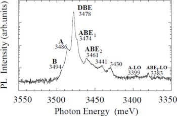
Fig.1 Low temperature (2K) PL spectrum of 80 μm thick GaN layer. The FWHM of the DBE peak is 2.3 meV.
In order to investigate the effect of growth rate on the crystalline quality of the layers, we determined the FWHM of the DBE line in the PL spectra as well as FWHM of (0002) reflection in XRD pattern using both ω−2θ and ω measurements. Their dependencies on the film thickness of GaN layers grown for different times at the same growth conditions are shown in Fig.2(a). Figure 2(b) presents these characteristics as a function of the growth rate. Information about the variation in the lattice parameter (i.e., degree of strain) [Reference Itoh and Okamoto6] and the dislocation distribution in the layers can be provided via the ω−2θ rocking curves. The FWHM obtained through a conventional ω-scan is due primarily to the variation in the mosaic spread.
Figure 2(a) shows, that increasing film thickness leads to an exponential decrease of the PL and ω−2θ linewidths. In changing the thickness from 15 to 96 μm, the FWHM of the exciton PL peak varies from 6.0 to 2.1 meV and ω−2θ FWHM values vary from 84 to 30 arcsec. These values indicate that the crystalline quality of the surface region of thick GaN HVPE films rivals the best GaN MOVPE layers. The narrowest ω-linewidth is 250 arcsec obtained for GaN layers with a thickness of 12 μm, one of the best values reported for GaN epitaxial layer grown without a buffer layer. Up to a critical thickness (dcrit) of about 42-48 μm, the (0002) reflection appears as a single peak (Fig.3a) in a ω-scan. The ω-FWHM value increases from 250 to 1000 arcsec with increasing thickness up to the dcrit . It is apparent that there is an increase in mosaic spread in thinner layers despite that the amount of stress in the layers decreases. In the thicker layers (over than dcrit), multiple peaks appear in the ω-scans (Fig.3b). A fitting procedure determined that each peak is comprised of several subpeaks with a FWHM values in the order of 250-350 arcsec, indicating the formation of several high quality domains.
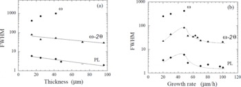
Fig.2 PL (meV) ana X-ray (arcsec) linewidths of GaN layers as a function of thickness (a) and growth rate (b). The dotted lines in Fig.2(b) are presented only as a guide to the eye and do not necessarily represent the specific functional relationship.
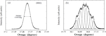
Fig.3 X-ray ω-scans of 12 μm (a) and 70 μm (b) thick GaN layers.
The dependence of the ω-FWHM on both the thickness and the growth rate are similar. At the same time, the dependencies of FWHM of both PL line and ω−2θ line versus growth rate show a more complicated behaviour (Fig.2b). In the beginning, increasing the growth rate results in a broadening of both linewidths. At further increasing the growth rate, both a multipeak appearance in the ω-scans and a dip in the PL and ω−2θ dependencies are simultaneously observed. The narrowing of these lines is indicative of improvement of crystalline quality of the material. It seems that there is a critical growth rate value Rcrit at which the behaviour of all dependencies is changed.
The surface topography images of the layers obtained by the optical microscopy show hillock type surfaces as illustrated by Fig.4 (a) and (b). The hillocks have a six-fold symmetry which is a typical feature for hexagonal crystals. The domains appear as single islands on the surface of the 12 μm thick GaN layer. Some of them are in the initial stage of development and some of them are further developed. The islands widen with increasing layer thickness and coalesce. Enlargement of a single island is limited by other islands and correspondingly when they meet boundaries are created. It is known that the boundaries have a high density of structural defects and they are an efficient source for more significant imperfections. In thinner films the increasing of both domain size and number results in broadening of the ω-curve. Further development of the hillock structure leads most probably to a domain appearance at the critical thickness of about 45 μm and to a tilting of the domains which can be seen as multipeaks in ω-scan. The domains might be formed over columnar structure crystallities which are expectable for heteroepitaxial growth without a buffer [Reference Akasaki, Amano, Koide, Haramatsu and Sawaki7] and we directly observed in our layers by cathodoluminescence imaging [Reference Goldys, Paskova, Ivanov, Arnaudov and Monemar8].
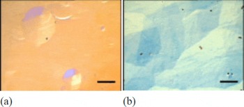
Fig.4 Optical micrographs of the growth surface of GaN layers with thickness of 12 μm (a) and 70 μm (b) grown at the same growth rate (25 μm/h).The marker represents 200 μm.
In the optical microscope, the surfaces of the domain-facets appear smooth. However, when the facets are imaged by AFM the presence of steps are revealed which are 30-80 nm wide and 5-6 Å high (Fig.5). As mentioned by Molnar et al. [Reference Molnar, Götz, Romano and Johnson2] this is indicative of a step-flow mode of growth. The step height corresponds to what one would expect for monoatomic steps (c = 5.19 Å). All samples grown at growth rate lower that Rcrit (about 60 μm/h) show such kind of morphology independent of thickness. The morphology of our thinner HVPE-GaN layer is similar to that observed by Rihrer et al. [Reference Rohrer, Payne, Qian, Skowronski, Doverspike, Rowland, Gaskill, Ponce, Dupuis, Nakamura and Edmond9] for 2.8 μm thick MOVPE grown GaN layers. However more pronounced domain structure is typical for our layers and taking into account that locally the growth remains two-dimensional on the top of each terrace or island, the HVPE growth can be considered in terms of a 2D multilayer model [Reference Greene10] with high lateral/vertical growth ratio.
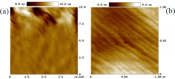
Fig.5 AFM micrographs of the surface of 70 μm thick GaN layer grown at 30 μm/h growth rate.
The morphology of GaN epilayers grown at higher growth rates exceeding the critical value was found to be completely different than for layers grown at lower growth rate. It is evident, even in optical microscope (Fig.6), that the domain facets are comprised of a huge number of small features.
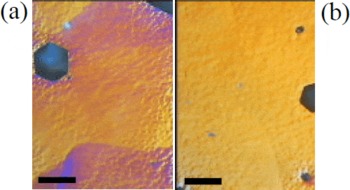
Fig.6 Optical microphotographs of two GaN layers grown at growth rate of 70 μm/h (a) and 80 μm/h (b). The marker represents 50 μm.
AFM images of thick layers (Fig.7) grown at 80 μm/h reveal the microstructure and show a presence of well-formed terraced hillocks. Two dimensional images of the layer surface (Fig.7b) reveal perfect flatness of every terraced step and very sharp boundaries between them with a height of ∼13nm. Terrace-bunching resulting in hillocks mediated by a screw dislocation in the centre was evident. Using higher magnification (Fig.7c) we can see that the microstucture of every terrace was formed by step-flow mode growth with a height of ∼10-13 Å.
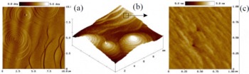
Fig.7 AFM micrographs of GaN layer grown at high growth rate (80 μm/h).
The growth mechanism of HVPE GaN layers grown at high growth rate is not exactly known; however the spiral growth model based on the existence of screw dislocations seems to be involved too. The 2D multilayer growth which is believed to be responsible for the background domain formation continues to be the favourite layer creator. However, at such high growth rates there is a comparative contribution of the spiral growth mode. The pronounced effect of the spiral growth might be related to a critical supersaturation of growth environment with GaCl. At low NH3/HCl ratio of 15:1 used (compared to commonly used 40:1 [Reference Naniwae, Itoh, Amano, Itoh, Hiramatsu and Akasaki3]), Ga droplets might be formed which can lead to the observed morphological features. In general, at growth rates exceeding the Rcrit value both growth mechanisms operate in a competitive way and the lateral/vertical growth ratio seems to be much lower than at low growth rate.
The 2D multilayer growth is the common growth mechanism for heteroepitaxy. Moreover for a system with high lattice mismatch between the substrate and the layer, islanding driven by an increasing strain component in the total system free energy usually leads to relaxation of the system [Reference Greene10]. So, the simultaneous operation of both mechanisms: 2D multilayer as a base and spiral growth which provides steps and enhances nucleation sites in the vicinity might explain the high growth rate approached as well as the improvement of structural characteristics with increasing the growth rate.
Conclusion
Thick HVPE-GaN epitaxial layers grown at growth rates between 20 and 105 μm/h were investigated. The layers exhibit in general a domain type structure with a slight misorientation. It was found that the domains are of high crystalline quality based on the values of structural characteristics. The HVPE growth of thick GaN layers proceeds via two growth mechanisms: 2D multilayer growth and spiral growth mechanism. The first one is completely dominant at low growth rate. At higher growth rate, both growth mechanisms operate in a competitive way.


