


Introduction
To study the distribution of elements in solids, X-ray mapping by scanning electron microscopes (SEMs) or electron microprobes has proved to be a quite convenient technique. These maps are obtained by scanning the electron beam (continuously or digitally) across the specimen surface to generate characteristic X-ray signals as a function of beam position. These signals are detected by a wavelength-dispersive or energy-dispersive spectrometer (WDS or EDS, respectively), which produces an X-ray spectrum, and the X-ray counts within a preselected energy range (that is, an element of interest) are used to trigger intensity on a cathode ray tube (CRT) or computer screen. Over time this process gives rise to a map of that element.
Historically, the beam was scanned continuously across the sample, generating a momentary bright flash (dot), captured directly on the photographic film of a camera attached to a CRT screen. This image, consisting of dots distributed along a number of image lines, is called an analog dot map. Analog maps suffer from a number of disadvantages: only one element at a time can be mapped, and no background subtraction is possible, just to mention two. Nevertheless, this method was used for 25 years, from the mid-1950s [Reference Cosslett and Duncumb1] to the end of the 1970s, when it was replaced by a new method, based on digitally rastering the electron beam [Reference Chambers2, Reference McCarthy3]. In these digital intensity maps the beam stops on a pixel, and the number of counts collected from an element for a given dwell time is recorded. The X-ray background may be subtracted, and an image can be formed of the X-ray intensity distribution for each of the elements selected. Presently, digital mapping is the only method in use for both the conventional Si(Li) detector and the newer silicon drift detector (SDD). More information about the X-ray mapping technique can be found in the review by Friel and Lyman [Reference Friel and Lyman4].
This article compares analog dot maps obtained with a WDS spectrometer at the end of the 1970s with digital intensity maps acquired with a modern SEM equipped with an SDD-EDS spectrometer. The sample for this comparison is a zirconium disc that was ion implanted, oxidized, and wedge-etched to detect the depth distribution of oxygen K X rays.
Materials and Methods
Ion-implanted and oxidized Zr sample
The same sample, previously prepared and analyzed in the 1970s [Reference Berti5, Reference Berti6] was used for this comparison. Briefly, it consists of a bulk polycrystalline zirconium disc, implanted with Ni ions at 150 keV to a dose of 5 × 10¹⁶ ions/cm2 and then oxidized in a dry oxygen flow at 450°C for 100 min. The objective of the work was to study the effect of implantation on the oxidation rate of Zr. Both X-ray microanalysis and Rutherford backscattering spectrometry (RBS), a depth profiling technique, were used to assess the oxidation. After the RBS measurements, to overcome the lack of depth sensitivity with X-ray microanalysis, the implanted and oxidized surface of the specimen was wedge thinned by means of a mechanical device as reported Armigliato et al. [7]. The maximum depth of etching was 1 µm, at an angle of 10-4 rad (see Figure 1). This allowed the depth of oxygen segregation at the Zr grain boundaries, as well as bulk grain oxidation, to be revealed in oxygen X-ray maps, thus confirming the interpretation of the corresponding RBS profiles.

Figure 1 BSE micrograph of the implanted and oxidized zirconium sample after the wedge-etching process (see text for details). The lighter etched region is a strip 1 mm wide.
The comparison maps were carried out on the same sample that was examined nearly 40 years ago. For the present X-ray microanalysis experiment, the surface of the sample was plasma-cleaned for 2 min in a Fischione instrument (Model 1020) to remove any surface hydrocarbon contamination.
Microanalysis details
An ARL-SEMQ microprobe was used in the 1970s to acquire oxygen maps of the sample described above. This instrument was equipped with a W filament and fully focusing WDS spectrometers; for the O K maps an RAP (Rb acid phtalate) crystal was used. The beam rastering was continuous (analog), so only dot mapping was possible.
The same sample was analyzed in a Zeiss LS-10 SEM, equipped with an LaB6 filament and a Bruker XFlash6 30 mm2 SDD detector. Analyses were obtained in the high-vacuum mode. The beam rastering was digital so the number of pixels and the size of the maps could be properly chosen. It is worth noting that this comparison between old and new oxygen maps was made possible by the practically unchanged sample conditions: the extremely low diffusion rate of oxygen at room temperature [Reference Rosa and Hagel8] corresponded to a negligible diffusion length after 37 years of less than a nanometer.
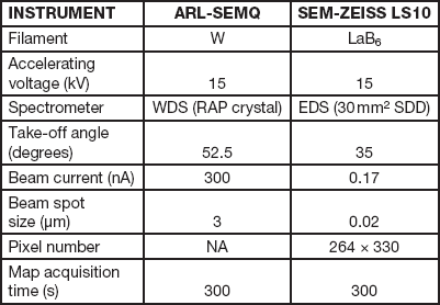
To compare results from the two instruments, both old and new oxygen maps were acquired at the same acceleration voltage (15 kV) and total acquisition time (300 s). Table 1 provides a summary of the experimental parameters used in the comparison.
Table 1 Values of experimental parameters employed for the acquisition of the oxygen maps in the two instruments used.
Results
Figure 1 shows a backscattered electron (BSE) image taken with the modern SEM of the original sample. The angle-etched region inside the implanted area appears as a 1 mm wide stripe. The etching depth increases from the top of the image to the bottom. The ZrO2 crystals observed in the etched region can be roughly divided into two groups: surfacial crystals only about 110 nm thick and bulk-like crystals averaging 230 nm thick. The estimated spatial resolution of X-ray maps is given by the Anderson-Hasler X-ray range, RX = 0.064(E0 1.68 - EC 1.68)/ρ, where E0 is the acceleration voltage, EC is the critical excitation energy of a characteristic X-ray line, and ρ is the average sample density [Reference Anderson and Hasler9]. In the present case E0 = 15kV, so RX was about 1 µm.
Figure 2 shows an example of the different quality of the images of the oxygen distribution obtained with the two instruments in a region inside the wedge, at a depth about 200 nm below the sample surface. These images include a single oxidized grain, about 20 µm in diameter and belonging to the thicker bulk-like group of crystals, surrounded by metallic Zr grains. The map on the left was obtained with a WDS on the ARL-SEMQ microprobe; whereas, that on the right was acquired by SEM-SDD instrument. The SEM-SDD oxygen map shows more detail including some oxidation along the Zr grain boundaries. The relatively poor spatial resolution of the older map is mostly due to the larger beam diameter (3 µm), a consequence of the 300 nA beam current. This high beam current was selected at that time to afford a short map acquisition time (300 s) in that instrument.

Figure 2 (Left) oxygen X-ray analog dot map, taken with the ARL-SEMQ microprobe in an area located at a depth of about 200 nm below the surface (adapted from [Reference Berti5]); (right) oxygen digital intensity map acquired with the SEM-SSD instrument at the same depth.
An additional comparison of map quality can be obtained by examining regions of the sample closer to the surface, where oxygen in the grain boundaries was detected by RBS [Reference Berti5]. Figure 3 shows that oxidation at grain boundaries was detected in X-ray maps from each instrument. Figure 3 (left) shows an oxygen map taken in older instrument of a Ti-implanted sample processed in the same way. While this map reveals oxygen in the grain boundaries, the apparent width of the oxygen segregation is several times that of the similar map taken with the modern SEM-SDD instrument. In the latter case the width of the oxygen segregation is close to the estimated Rx value, that is, about 1 µm.

Figure 3 (Left) oxygen analog X-ray map taken with the ARL-SEMQ microprobe (adapted from [Reference Berti5]) at a shallower depth than Figure 2. (Right) oxygen digital X-ray map acquired with the SEM-SSD instrument.
Discussion
The comparison of oxygen mapping capabilities for the two instruments clearly shows the great progress achieved in instrumentation from the late 1970s to present. The new images reported here were obtained using experimental conditions that were inevitably somewhat different for the two instruments: (a) the gun filament (W in ARL-SEMQ, LaB6 in SEM), (b) the detection efficiency in terms of count rate per nA, (c) the peak/background ratios, and (d) the take-off angle (Table 1). Among these, only the last two were more favorable for the WDS-ARL microprobe. In any case, in terms of resolution and contrast, the oxygen X-ray maps obtained with the SEM-SDD are clearly superior. It also should be noted that at the time of the earlier measurements, conventional Si(Li) EDS systems did not employ X-ray windows thin enough to allow transmission of low-energy oxygen X-rays (525 eV).
Conclusion
This work shows the marked improvement in the quality of oxygen X-ray maps, acquired with a state-of-the-art SEM equipped with an SDD-EDS spectrometer, compared to those obtained more than three decades ago with an electron microprobe equipped with a WDS spectrometer. For this comparison the same sample, stored for 37 years, was used. It consisted of a bulk zirconium disc, ion-implanted, and oxidized.
Acknowledgements
The authors are indebted to G.G. Bentini, A. Garulli, and R. Rinaldi for useful discussions and to the ProAmbiente Technopole of the Emilia-Romagna region of Italy for the use of the Zeiss LS10 SEM-EDS instrument.


