


Introduction
In many materials, accurate modeling of the energy loss near-edge structure (ELNES) in electron energy-loss spectroscopy (EELS) is impossible without considering core hole interactions. The positively charged core hole localizes the final state electron wavefunction at the excited atom, causing an increase in intensity at the EELS edge onset, as well as a shift to lower energy loss (Duscher et al., Reference Duscher, Buczko, Pennycook and Pantelides2001; Mizoguchi et al., Reference Mizoguchi, Olovsson, Ikeno and Tanaka2010). Core holes have been shown to alter the ELNES of semiconductor and insulator materials (Altarelli & Dexter, Reference Altarelli and Dexter1972; Batson, Reference Batson1993; Nufer et al., Reference Nufer, Gemming, Elsässer, Köstlmeier and Rühle2001; van Benthem et al., Reference van Benthem, Elsässer and Rühle2003; Jiang & Spence, Reference Jiang and Spence2004) and, to a lesser extent, metals as well (Luitz et al., Reference Luitz, Maier, Hébert, Schattschneider, Blaha, Schwarz and Jouffrey2001). Several theories have been put forward to describe the conditions leading to a strong core hole interaction. Gao et al. (Reference Gao, Pickard, Payne, Zhu and Yuan2008) found that for a given ionic compound core hole effects were stronger in the cations than anions, and therefore suggested that electronegativity and valence electron screening were important parameters. Mauchamp et al. (Reference Mauchamp, Jaouen and Schattschneider2009) however proposed that core hole effects are governed by the spatial localization of empty states above the Fermi level and the angular momentum of the unoccupied states at the core hole atom in its excited state configuration. On the other hand, Mendis & Ramasse (Reference Mendis and Ramasse2021) recently developed an electrodynamic model where the work done in separating the incident, high energy electron from the (dynamically screened) core hole is calculated. Since the incident electron and core hole have opposite charges, the extra work done results in an energy gain correction, which can be deconvolved from the EELS measurement to give a “fully screened” spectrum that is, in principle, free from core hole effects.
Much of the work on EELS core hole modeling has been on bulk materials, with less emphasis on confined geometries, such as nanoparticles, free surfaces, or interfaces. High spatial and energy resolution EELS measurements can now provide unprecedented insight into the detailed local bonding environment of solids (see, e.g., Lagos et al., Reference Lagos, Trügler, Hohenester and Batson2017; Hachtel et al., Reference Hachtel, Huang, Popovs, Jansone-Popova, Keum, Jakowski, Lovejoy, Dellby, Krivanek and Idrobo2019; Hage et al., Reference Hage, Kepaptsoglou, Ramasse and Allen2019), and therefore understanding core hole effects in non-periodic systems is essential for correct interpretation of data. As an example, core hole screening by valence electrons for (say) a free surface will be different from the bulk material, since the electrostatic potential must satisfy Maxwell's boundary conditions at the free surface. In fact, reflection EELS measurements have shown that the ELNES at the surface is different from bulk (Henrich et al., Reference Henrich, Dresselhaus and Zeiger1976; Margaritondo & Rowe, Reference Margaritondo and Rowe1977). Surface core hole effects can be simulated either using electronic structure methods or by modifying the electrodynamic model (Mendis & Ramasse, Reference Mendis and Ramasse2021) for the given boundary conditions. The former method is, however, computationally expensive, since large supercell sizes are required due to the material geometry being intrinsically non-periodic, and because the interaction between neighboring core holes must also be minimized (Seabourne et al., Reference Seabourne, Scott, Vaughan, Brydson, Wang, Ward, Wang, Kohn, Mendis and Petford-Long2010).
In this work, the surface core hole fine structure in MgO core-loss edges is investigated both experimentally and theoretically. MgO smoke cubes are examined using spatially resolved EELS in a scanning transmission electron microscope (STEM). A STEM probe incident along an end-on face of the MgO cube is used to measure the surface electronic structure. MgO is a large band gap (~7.9 eV; Williams & Arakawa, Reference Williams and Arakawa1967) insulator that shows strong core hole effects in Mg L, K, and O K-EELS edges (Lindner et al., Reference Lindner, Sauer, Engel and Kambe1986; O'Brien et al., Reference O'Brien, Jia, Dong, Callcott, Rubensson, Mueller and Ederer1991; Duscher et al., Reference Duscher, Buczko, Pennycook and Pantelides2001; Elsässer & Kostlmeier, Reference Elsässer and Kostlmeier2001; Mizoguchi et al., Reference Mizoguchi, Olovsson, Ikeno and Tanaka2010; Seabourne et al., Reference Seabourne, Scott, Vaughan, Brydson, Wang, Ward, Wang, Kohn, Mendis and Petford-Long2010). The Mg L-edge in MgO also shows subtle surface ELNES, which has been attributed to non-degenerate energy levels due to a surface electric field (i.e., Stark effect; Henrich et al., Reference Henrich, Dresselhaus and Zeiger1976). The electric field arises because of different Madelung potentials for surface versus bulk atoms. MgO is, therefore, an excellent system for exploring surface core hole effects. The paper is organized as follows: the electrodynamic model of Mendis & Ramasse (Reference Mendis and Ramasse2021) is first extended to include surface boundary conditions. As will be seen below, electrodynamic theory provides a computationally efficient method to model surface core hole interactions, while at the same time providing physical insight into the screening mechanisms operating at a free surface. The theory is used to analyze the experimental results for O K- and Mg L3,2-edges. A strong surface core hole fine structure is observed for the former, while any changes to the Mg L3,2-edge are below the energy resolution of the measurement. The results demonstrate the importance of the dielectric environment (in this case a free surface, but also includes interfaces between two different materials) on the observed ELNES.
Materials and Methods
Electrodynamic Model of Surface Core Hole Screening
In this section, the work done in separating the incident, high energy electron from a core hole located close to a free surface is calculated. The scattering geometry is illustrated in Figure 1a. The incident electron is traveling along the z-axis with speed v in a semi-infinite slab which has a free surface at x = −s, parallel to the yz-plane. The core hole has impact parameter (b x, −b y) in the xy-plane and has z-coordinate −z 0 at time t = 0 when it first appears; that is, z 0 is the distance the incident electron travels during the time it takes for the electronic transition to happen. By the time-energy form of the uncertainty principle  $z_0\sim ( {v\hbar /{\rm \Delta }E} )$, where $\hbar$ is Planck's reduced constant and ΔE is the energy loss. Quantum mechanics predicts that the probability for core hole formation increases gradually with time, so that the assumption the core hole appears at a fixed point in time is an approximation (Mendis & Ramasse, Reference Mendis and Ramasse2021). It is also assumed that the energy loss ΔE is small enough to have a negligible effect on the high energy electron trajectory (a condition that is reasonably satisfied in EELS), and therefore, the work done is equal to the change in electrostatic potential energy. If $\phi ( {\bf{r}}, \;t)$ is the instantaneous potential at position vector r due to the core hole, the work δW done over an infinitesimal path of the electron trajectory is
 $$\delta W = {-}q_{\rm e}\left[{\displaystyle{{\partial \phi } \over {\partial t}}\delta t + \displaystyle{{\partial \phi } \over {\partial z}}\delta z} \right] = {-}q_{\rm e}\left[{\displaystyle{{\partial \phi } \over {\partial t}} + v\displaystyle{{\partial \phi } \over {\partial z}}} \right]\delta t,$$
where q e is the magnitude of the electronic charge. Using inverse Fourier transforms,
 $$\displaystyle{{\partial \phi } \over {\partial t}} = \displaystyle{1 \over {2\pi }}\int -i\omega \phi ( x, \;{\bf q}_{yz}, \;\omega ) {\rm exp}[ {2\pi i{\bf q}_{yz}\cdot {\bf r}_{yz}-i\omega t} ] d{\bf q}_{yz}d\omega, $$
 $$\displaystyle{{\partial \phi } \over {\partial z}} = \displaystyle{1 \over {2\pi }}\int 2\pi iq_z\phi ( x, \;{\bf q}_{yz}, \;\omega ) {\exp}[ {2\pi i{\bf q}_{yz}\cdot {\bf r}_{yz}-i\omega t} ] d{\bf q}_{yz}d\omega $$
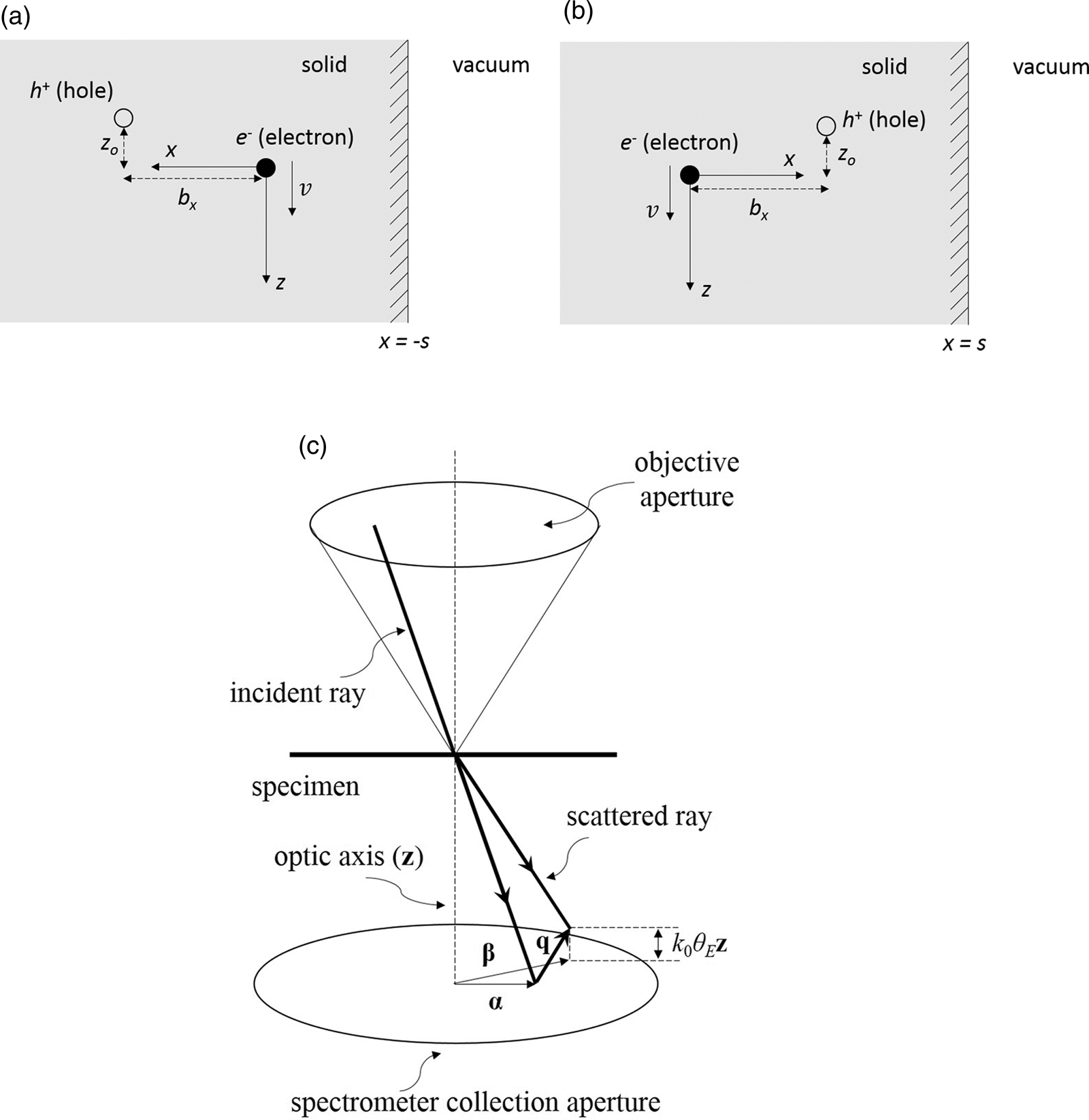
Fig. 1. (a,b) Different scattering geometries for the core hole interaction in a semi-infinite solid. The incident electron is traveling along the z-axis with speed v. The core hole is at a distance b x along the x-axis, and at its moment of creation is at z = −z 0 along the z-axis. The free surface is at x = −s for (a) and x = s for (b). (c) Schematic of the STEM scattering geometry. An incident ray with transverse wavevector α is inelastically scattered to the transverse wavevector β with scattering vector q. Only scattered rays within the EELS spectrometer entrance aperture are detected.
with  ${\bf q}_{yz}$ and q z being the components of the scattering vector q in the yz-plane and along the z-axis, respectively. ω is the angular frequency and ${\bf r}_{yz}$ is the component of r in the yz-plane. Substituting in (1) and integrating along the electron trajectory x, y = 0, z = vt gives an expression for the total work done W(b x, −b y):
 $$\!\!\eqalign{&W( {b_x, \;-b_y} )\cr &\quad ={-}\displaystyle{{iq_{\rm e}} \over {2\pi }}\int_0^\infty {\left\{{\int ( {2\pi q_zv-\omega } ) \phi ( 0, \;{\bf q}_{yz}, \;\omega ) e^{i( {2\pi q_zv-\omega } ) t}d{\bf q}_{yz}d\omega } \right\}dt}.} $$
Note that the infinite upper limit for the time integral does not take into account the lifetime of the core hole. However, for EELS edges, the lifetime is sufficiently long for the swift, incident electron to be far enough from the core hole such that the Coulomb interaction has decreased to a negligible value (Mendis & Ramasse, Reference Mendis and Ramasse2021). Ignoring the finite core hole lifetime is, therefore, justified. The time integral has the solution
 $$\!\!\eqalign{&\int_0^\infty {e^{i( {2\pi q_zv-\omega } ) t}dt}\cr &\quad = {\int_{-\infty }^\infty {H( t ) e^{i( {2\pi q_zv-\omega } ) t}dt = \pi \delta ( {2\pi q_zv-\omega } ) + \displaystyle{i \over {( {2\pi q_zv-\omega } ) }}} }, $$
where H(t) is the Heaviside unit step function and δ is the Dirac delta function. Therefore,
 $$W( {b_x, \;-b_y} ) = \displaystyle{{q_{\rm e}} \over {2\pi }}\int \phi ( {0, \;{\bf q}_{yz}, \;\omega } ) d{\bf q}_{yz}d\omega. $$
 The potential ϕ is obtained from Poisson's equation,  $\varepsilon _0\varepsilon ( \omega ) \nabla ^2\phi ( {{\bf r}, \;t} ) = {-}\rho _f( {{\bf r}, \;t} ),$ which can also be expressed using Fourier transforms as:
 $$\varepsilon _0\varepsilon ( \omega ) \left[{\displaystyle{{\partial^2} \over {\partial x^2}}-4\pi^2q_{yz}^2 } \right]\phi ( {x, \;{\bf q}_{yz}, \;\omega } ) = {-}\rho _f( {x, \;{\bf q}_{yz}, \;\omega } ) ,$$
where  $\rho _f( {{\bf r}, \;t} ) = q_{\rm e}\delta ( {x-b_x} ) \delta ( {y + b_y} ) \delta ( {z + z_0} ) H( t )$ is the core hole free charge density, ɛ 0 is the permittivity of free space, and ɛ(ω) is the dielectric function in the local approximation. Fourier transforming $\rho _f( {{\bf r}, \;t} )$ and substituting in equation (6) gives:
 $$\!\!\eqalignb{&\left[{\displaystyle{{\partial^2} \over {\partial x^2}}-4\pi^2q_{yz}^2 } \right]\phi ( {x, \;{\bf q}_{yz}, \;\omega } )\cr & \quad ={-}\displaystyle{{q_{\rm e}\delta ( {x-b_x} ) } \over {\varepsilon _0\varepsilon ( \omega ) }}\exp ( {2\pi i{\bf q}_{yz}\cdot {\bf R}} ) \left[{\pi \delta ( \omega ) + \displaystyle{i \over \omega }} \right].}$$
 The position vector  ${\bf R}$ lies in the yz-plane and has components (b y, z 0). The solution for $\phi ( {x, \;{\bf q}_{yz}, \;\omega } )$ within the solid is, therefore, given by:
 $$\!\!\eqalignb{\phi ( {x, \;{\bf q}_{yz}, \;\omega } ) &= a\exp ( {-2\pi q_{yz}x} ) +\displaystyle{{q_{\rm e}\exp ( {-2\pi q_{yz}\vert {x-b_x} \vert } ) } \over {4\pi \varepsilon _0\varepsilon ( \omega ) q_{yz}}}\cr &\quad \times \exp ( {2\pi i{\bf q}_{yz}\cdot {\bf R}} ) \left[{\pi \delta ( \omega ) + \displaystyle{i \over \omega }} \right]}$$
with a being a constant. The | | symbol represents the absolute value of a number. Equation (8) satisfies the boundary condition that the potential is zero for x → ∞ (Fig. 1a). Outside the solid, that is, in vacuum, there is no core hole and equation (6) becomes
 $$\left[{\displaystyle{{\partial^2} \over {\partial x^2}}-4\pi^2q_{yz}^2 } \right]\phi _{\rm v}( {x, \;{\bf q}_{yz}, \;\omega } ) = 0.$$
ϕ v represents the potential in vacuum. A suitable solution to equation (9), which also satisfies the boundary condition that ϕ v must be zero for x → −∞ is
 $$\phi _{\rm v}( {x, \;{\bf q}_{yz}, \;\omega } ) = b\exp ( {2\pi q_{yz}x} ), $$
where the constant b, along with a, can be determined from Maxwell's boundary conditions for the electric field; that is
 $${\phi ( {x, \;{\bf q}_{yz}, \;\omega } ) } \vert _{x = {-}s} = {\phi_{\rm v}( {x, \;{\bf q}_{yz}, \;\omega } ) } \vert _{x = {-}s},$$
 $$\left. {\varepsilon ( \omega ) \displaystyle{{\partial \phi ( {x, \;{\bf q}_{yz}, \;\omega } ) } \over {\partial x}}} \right\vert _{x = {-}s} = \left. {\displaystyle{{\partial \phi_{\rm v}( {x, \;{\bf q}_{yz}, \;\omega } ) } \over {\partial x}}} \right\vert _{x = {-}s}.$$
 Substituting the resulting expression for  $\phi ( {x, \;{\bf q}_{yz}, \;\omega } )$ in equation (5) gives
 $$\!\!\eqalign{W( {b_x, \;-b_y} ) &= \displaystyle{{q_{\rm e}^2 } \over {8\pi ^2\varepsilon _0}}\int \displaystyle{{e^{2\pi i{\bf q}_{yz}\cdot {\bf R}}} \over {q_{yz}}}\displaystyle{{\left[{\pi \delta ( \omega ) + \displaystyle{i \over \omega }} \right]} \over {\varepsilon ( \omega ) }}\cr&\quad\times \left\{{\left({\displaystyle{{\varepsilon ( \omega ) -1} \over {\varepsilon ( \omega ) + 1}}} \right)e^{{-}2\pi q_{yz}( {b_x + 2s} ) } + e^{{-}2\pi q_{yz}b_x}} \right\}d{\bf q}_{yz}d\omega.} $$
First consider the ω-integral, which has integration limits between −∞ and ∞. Using the fact that the dielectric function is a real quantity and hence ɛ( − ω) = ɛ(ω)*, where the asterisk denotes the complex conjugate, we obtain:
 $$\!\!\eqalign{W( {b_x, \;-b_y} ) &= \displaystyle{{q_{\rm e}^2 } \over {4\pi ^2\varepsilon _0}}\int \displaystyle{{e^{2\pi i{\bf q}_{yz}\cdot {\bf R}}} \over {q_{yz}}} \cr &\quad \times \left\{{\pi {\rm Re}[ {F( 0 ) } ] + \int_{\omega = 0}^\infty {\displaystyle{{{\rm Im}[ {-F( \omega ) } ] } \over \omega }d\omega } } \right\}d{\bf q}_{yz},}$$
 $$F( \omega ) = \displaystyle{1 \over {\varepsilon ( \omega ) }}\left\{{\left({\displaystyle{{\varepsilon ( \omega ) -1} \over {\varepsilon ( \omega ) + 1}}} \right)e^{{-}2\pi q_{yz}( {b_x + 2s} ) } + e^{{-}2\pi q_{yz}b_x}} \right\}.$$
 Here “Re” and “Im” denote the real and imaginary parts of a complex number, respectively. Representing  ${\bf q}_{yz}$ in polar coordinates (q yz, α), we have $d{\bf q}_{yz} = q_{yz}dq_{yz}d\alpha$. Integrating equation (13a) over the polar angle α finally gives
 $$\!\!\eqalign{&W( {b_x, \;-b_y} )\cr &\quad = \displaystyle{{q_{\rm e}^2 } \over {2\pi \varepsilon _0}}\int J_0( {2\pi q_{yz}R} ) \left\{{\pi {\rm Re}[ {F( 0 ) } ] + \int_{\omega = 0}^\infty {\displaystyle{{{\rm Im}[ {-F( \omega ) } ] } \over \omega }d\omega } } \right\}dq_{yz},}$$
where J 0 is the zero order Bessel function of the first kind. The first term represents the static (i.e., ω = 0) core hole screening contribution, while the second term is due to dynamic (i.e., ω ≠ 0) screening. Equation (14) has a similar mathematical form to the work done in a bulk solid (see equation (13) in Mendis & Ramasse, Reference Mendis and Ramasse2021), apart from the function F(ω), which replaces [1/ɛ(ω)]. Let us examine F(ω) in more detail. Equation (13b) is reminiscent of a begrenzung or boundary effect (Howie & Milne, Reference Howie and Milne1984), with the first and second terms representing surface and bulk contributions, respectively; clearly, the larger the value of s, the smaller the surface contribution, as required. The term x im = b x + 2s in the first exponential of equation (13b) is also significant, since it represents the distance along the x-axis between the core hole and image charge of the incident electron on the vacuum side of the free surface (Fig. 1a). From the “method of images” (Jackson, Reference Jackson1998), it therefore follows that the surface term in equation (13b) is due to the image charge −[(ɛ(ω) − 1)/(ɛ(ω) + 1)]q e of the incident electron. The work done can also be calculated for the scattering geometry depicted in Figure 1b, that is, with the core hole between the free surface and the incident electron (cf., Fig. 1a), using the method outlined here. The result has a similar form to equation (14), the only difference being that x im = 2s − b x for the distance between the image charge and core hole.
Equation (14) represents the work done for a single impact parameter  ${\bf b} = ( {b_x, \;-b_y} )$, while in practice there will be a range of impact parameters that are determined by the illumination and measurement conditions. For STEM EELS, the impact parameter distribution is given by (Kohl & Rose, Reference Kohl and Rose1985):
 $$\!\!\eqalignb{P( {\bf b} )& \propto \int A( {\bf \alpha } ) A( {{\bf {\alpha }^{\prime}}} ) D( {\bf \beta } ) e^{i[ {\chi ( {{\bf {\alpha }^{\prime}}} ) -\chi ( {\bf \alpha } ) } ] }e^{2\pi i{\bf b}\cdot ( {{\bf {\alpha }^{\prime}}-{\bf \alpha }} ) }\cr &\quad\times \displaystyle{{S( {{\bf q}, \;{\bf {q}^{\prime}}, \;{\rm \Delta }E} ) } \over {q^2{{q}^{\prime}}^2}}d^2{\bf \alpha }d^2{\bf \alpha }^{\prime}d^2{\bf \beta },}$$
where χ is the lens aberration function and  $S( {{\bf q}, \;{\bf {q}^{\prime}}, \;{\rm \Delta }E} )$ is the dynamic form factor, which is proportional to ${\bf q}\cdot {\bf {q}^{\prime}}$ for non-magnetic atoms in the dipole limit (Muller & Silcox, Reference Muller and Silcox1995). α, α′ are any two transverse STEM probe wavevectors and β is a wavevector within the EELS spectrometer aperture (Fig. 1c). A(α) and D(β) are the aperture functions for the STEM probe and EELS spectrometer, respectively. In the small angle, small energy-loss limit the scattering vector ${\bf q}$ is given by [k oθE z + (β – α)], where k o is the wavenumber of the incident electrons of primary energy E o, θE is the characteristic scattering angle (=ΔE/2E o), and z is a unit vector along the optic axis (Egerton, Reference Egerton1996). A similar expression is valid for the scattering vector ${\bf {q}^{\prime}}$, but with α′ replacing α.
The procedure for calculating core hole effects is as follows. The work done at a given impact parameter is determined by equation (14), with the upper limit for the q yz integral set by the EELS spectrometer entrance aperture. Strictly speaking, this is an approximation, since the EELS aperture is defined in the  ${\bf q}_{xy}$ reciprocal plane, not ${\bf q}_{yz}$. For small energy losses however, the scattering is predominantly in the forward direction, so that the error will be small. Furthermore, equation (14) assumes that the incident electrons are traveling along the optic z-axis and does not take into account the STEM probe convergence angle. This is, however, not important for the milli-radian probe angle used in this study (Howie & Milne, Reference Howie and Milne1984). The dielectric function ɛ(ω) in equation (14) can be determined by a Kramers–Kronig analysis of the low-loss EELS spectrum (Egerton, Reference Egerton1996). The work done represents the energy gain for the impact parameter of interest, and the corresponding intensity is given by $P( {\bf b} )$ in equation (15). In this way, an energy gain spectrum can be constructed for all allowed impact parameters. For a given STEM probe position, the two scattering geometries shown in Figures 1a and 1b must both be considered, since they are both allowed. However, in this work, only the special case where the STEM probe is incident along the free surface (i.e., s = 0) is analyzed, so that the scattering geometry in Figure 1b is not applicable. The calculated energy gain spectrum is deconvolved from the background subtracted EELS edge to give a “fully screened” spectrum that should, in principle, be free of core hole effects.
Experimental Procedure
MgO nanocubes were prepared by burning Mg ribbon (99.5% purity, as stated by the supplier, Sigma-Aldrich) in air and collecting the smoke particles onto a holey carbon grid. The sample was examined in a 200 kV, JEOL 2100F field emission gun transmission electron microscope operating in STEM mode with 7.2 mrad probe semi-convergence angle. The probe angle is smaller than the Scherzer optimum value, meaning that the probe size is diffraction limited. EELS spectra were acquired at 0.2 eV/channel dispersion using a Gatan GIF Tridiem spectrometer with 7.2 mrad collection semi-angle. The energy resolution, as measured from the full-width at half-maximum of the zero-loss peak, was 1.6 eV. The spectrometer does not have a dual-EELS mode, and therefore, low-loss and O K core-loss spectrum images had to be acquired separately. This inevitably results in a slight mismatch in the spatial registry of the two data sets, although care was taken to minimize the error. During spectrum imaging, the STEM dark-field (DF) and EELS signals were acquired simultaneously. Prior to acquisition, the MgO cube was tilted to the [001]-zone axis, so that four of the six cube faces were end-on to the STEM probe, thereby enabling EELS measurements of free surfaces. Only MgO cubes suspended over vacuum were selected. Since the cube is held in place by only weak van der Waals forces between neighboring material (i.e., holey carbon or other MgO cubes), there was a slight shifting away from the ideal [001]-orientation during acquisition. This is especially true for the core-loss spectrum images, which have a longer acquisition time. The misorientation will have only a small effect on the measurement so long as the tilt axis is largely parallel to the scan direction, since then the cube faces of interest remain end-on to the STEM probe. Specimen tilt was monitored by acquiring STEM bright-field (BF) and DF images before and after EELS acquisition. An inclined cube face can be identified by an increase in projected width, or in more extreme cases, by thickness fringes in the STEM-BF image.
Results and Discussion
Dielectric Function and Surface Plasmon Modes of MgO Cubes
Figures 2a and 2b show simultaneously acquired STEM-BF and DF images of a MgO cube attached to a larger cube (top left) and suspended over vacuum. The MgO cube of interest is near the [001]-orientation. The top and bottom cube faces show projected width in the STEM-BF image, although the left and right faces are closer to being end-on. The cube dimension is 81.5 ± 0.3 nm. A low-loss EELS spectrum image was acquired along the horizontal line annotated in Figure 2b, which passes through roughly the middle of the cube. The STEM-DF intensity profile, acquired simultaneously with the EELS spectrum image, is shown in Figure 2c. Defining the cube edge as being the midpoint of the DF-intensity “step,” a value of 82.1 ± 0.7 nm is extracted for the cube size from Figure 2c. This is similar to the result obtained from the STEM images, which suggests that the spatial drift during low-loss EELS line spectrum imaging is small.

Fig. 2. (a,b) STEM-BF and DF images of a MgO cube suspended over vacuum. The horizontal line in (b) indicates the region over which a low-loss EELS spectrum image was acquired. The DF-signal acquired simultaneously with the spectrum image is shown in (c). (d) The low-loss EELS spectrum extracted from the interior (“bulk”) of the cube, while (e,f) show the dielectric function and effective number of electrons plot obtained from a Kramers–Kronig analysis.
The intensity plateau region in Figure 2c was used to obtain a low-loss EELS spectrum for “bulk” MgO by summing individual spectra over a 20 nm spatial range. The extracted spectrum is shown in Figure 2d. A Kramers–Kronig analysis gives the real (ɛ 1) and imaginary (ɛ 2) parts of the dielectric function (Fig. 2e) and effective number of electrons as a function of energy loss (Fig. 2f). The Kramers–Kronig derived specimen thickness is 73.7 nm, which is close to the true value of 81.5 nm. The dielectric function for MgO single crystals has been previously reported by Williams & Arakawa (Reference Williams and Arakawa1967) and by Roessler & Walker (Reference Roessler and Walker1967) using optical reflectance measurements. The EELS extracted dielectric function (Fig. 2e) shows similar gross features to the optical results, although there are important differences. For example, the onset of ɛ 2 for the EELS data is at 4.0 eV, significantly below the band gap value of 7.9 eV (Williams & Arakawa, Reference Williams and Arakawa1967). This is likely to be due to Čerenkov radiation (Stöger-Pollach et al., Reference Stöger-Pollach, Franco, Schattschneider, Lazar, Schaffer, Grogger and Zandbergen2006), since from the static ɛ 1 value (Fig. 2e), the 200 kV electron exceeds the phase velocity of light within MgO. Furthermore, ɛ 2 in the optical data showed a sharp peak at 7.6 eV, slightly below the band gap, which was attributed to excitons (Roessler & Walker, Reference Roessler and Walker1967). No such peak is observed with EELS. This could be due to the sample quality between the two studies; the optical measurements were carried out on single crystals, while the EELS data are for MgO smoke cubes that are likely to be non-stoichiometric and therefore lower crystal quality. The large peak at 22.6 eV in the low-loss spectrum (Fig. 2d) is the bulk plasmon, since the ɛ 1 curve shows a zero-crossing at 21.2 eV with positive slope (Fig. 2e; Egerton, Reference Egerton1996). The mismatch in energies and the weak nature of the zero-crossing is due to interband transitions around the plasmon energy. Similar results are also observed in optical measurements of MgO single crystals (Roessler & Walker, Reference Roessler and Walker1967; Williams & Arakawa, Reference Williams and Arakawa1967). The small peak at ~15 eV in the low-loss spectrum (Fig. 2d) could be interpreted as a surface plasmon, since it is lower than the bulk plasmon energy by approximately a factor of (1/√2). However, this peak is also observed in the bulk energy-loss function, Im[ − 1/ɛ(ω)], calculated using optical data (Roessler & Walker, Reference Roessler and Walker1967; Williams & Arakawa, Reference Williams and Arakawa1967), and is therefore due to interband transitions, as evidenced by the large ɛ 2 values in this energy range (Fig. 2e). Finally, assuming Mg and O each have 2 (i.e., 3s 2) and 6 (i.e., 2s 22p 4) valence electrons respectively, the valence electron density for MgO with rock salt crystal structure is 429 electrons per nm3. If the oxygen valence electrons are limited to only 2p electrons, the number density is reduced to 322 electrons per nm3. From Figure 2f however, the effective number of electrons at 30 eV (i.e., the high energy limit of the plasmon peak) is only 236 electrons per nm3. This large discrepancy has been observed in optical measurements as well and has been attributed to interband transitions above the plasmon energy (Williams & Arakawa, Reference Williams and Arakawa1967).
A low-loss EELS spectrum image was also acquired across the entire MgO cube to map the surface plasmon modes, which were extracted using principal component analysis (Bosman et al., Reference Bosman, Watanabe, Alexander and Keast2006). The STEM-DF image acquired simultaneously with the EELS spectrum image is shown in Figure 3a and indicates some drifting of the nanoparticle during measurement. Figures 3b and 3c show the “score images” for the first and third principal components, respectively. A score image indicates the sample regions where a given principal component has a strong weighting and can be used to extract unique spectral features from the data set, which are otherwise difficult to identify manually (Mendis et al., Reference Mendis, Taylor, Guennou, Berg, Arasimowicz, Ahmed, Deligianni and Dale2018). It is clear that Figures 3b and 3c reveal edge and corner low-loss spectra, respectively. In Figure 3c, the top left corner has reduced weighting, due to the fact that this corner is attached to a neighboring MgO cube (Figs. 2a, 2b), thereby changing its dielectric environment. Low-loss EELS spectra were extracted from the right face edge and bottom right corner of the cube and superimposed with the “bulk” spectrum in Figure 3d. The edge and corner spectra have higher intensity at energy losses below the bulk plasmon peak due to surface plasmon modes. This is consistent with the surface loss function, Im[ − 1/(1 + ɛ(ω))], calculated using optical data (Williams & Arakawa, Reference Williams and Arakawa1967), as well as EELS simulations of the corner modes (Aizpura et al., Reference Aizpura, Howie and Garcia de Abajo1999). The surface losses are larger at the edges compared with cube corners. To determine the extent of surface plasmon delocalization, the signal intensity within a 10–17 eV energy window was plotted as a function of position, using the line spectrum image data from Figure 2b. The result is shown in Figure 3e. Note that the intensity in the middle of the cube does not decrease to zero, since from Figure 3d, the “bulk” EELS spectrum contains interband transitions within the 10–17 eV energy window. The signal intensity peaks at the cube edges and is asymmetrical, with the right cube face having a higher intensity compared with the left face. It is not clear if this is an intrinsic property for this particular cube, or an extrinsic effect due to cube misorientation and/or the left face having a slightly different dielectric environment, due to it being closer to the larger MgO cube in the top left corner of Figures 2a and 2b. The decay of the signal intensity from the left and right cube faces into the vacuum region is plotted on a logarithmic scale in Figure 3f. The curves are not perfectly linear, which is to be expected, since the 10–17 eV energy range spans several surface plasmon modes and interband transitions, each with its own unique characteristic decay length. Nevertheless, a straight line was fitted to the graph between 5 and 15 nm, and from the gradient decay lengths of 9.5 ± 0.3 nm and 8.0 ± 0.2 nm were obtained for the left and right cube faces, respectively.

Fig. 3. (a) The STEM-DF signal acquired during low-loss EELS spectrum imaging over the area of the MgO cube. The “score” images for the first and third principal components of the spectrum image data set are shown in (b,c), respectively. In (d), representative EELS spectra for the cube edge and corner regions are shown superimposed with the “bulk” spectrum. The intensity of the bulk plasmon peak is normalized for a direct comparison. (e) The surface loss intensity within a 10–17 eV energy window plotted as a function of position. In (f), the intensity on the vacuum side is plotted on a logarithmic scale as a function of distance from the left/right cube face.
O K-Edge Surface Core Hole Fine Structure
A separate line spectrum image for the O K-edge was acquired across a similar region of the MgO cube to that shown in Figure 2b. Using the simultaneously acquired DF-signal as a guide the O K-edges from the “bulk” region, as well as left and right cube faces were extracted. These are shown superimposed in Figure 4a. Consider first the bulk O K-edge. The first broad peak at ~537 eV is known to be a doublet (Lindner et al., Reference Lindner, Sauer, Engel and Kambe1986; Duscher et al., Reference Duscher, Buczko, Pennycook and Pantelides2001; Seabourne et al., Reference Seabourne, Scott, Vaughan, Brydson, Wang, Ward, Wang, Kohn, Mendis and Petford-Long2010), although the energy resolution here is insufficient to observe the splitting. Ground state electronic structure calculations, where no core hole is included, produce only a single peak at approximately the same energy as the high energy peak of the doublet (Duscher et al., Reference Duscher, Buczko, Pennycook and Pantelides2001; Seabourne et al., Reference Seabourne, Scott, Vaughan, Brydson, Wang, Ward, Wang, Kohn, Mendis and Petford-Long2010). The doublet is, therefore, due to the core hole interaction. Core hole effects can be largely removed from bulk spectra using the electrodynamic method of Mendis & Ramasse (Reference Mendis and Ramasse2021). The impact parameter distribution, P(b), for the O K-edge is shown in Figure 4b, and was calculated for the experimental conditions used in this study (i.e., 200 kV focussed, diffraction limited STEM probe with 7.2 mrad semi-convergence angle and 7.2 mrad EELS collection semi-angle). Note that the impact parameter can be as large as a few Angstroms for the O K-edge. The energy gain spectrum for the O K-edge in bulk MgO was calculated using equation (13) in Mendis & Ramasse (Reference Mendis and Ramasse2021), using as inputs the experimentally derived dielectric function (Fig. 2e) and P(b) distribution (Fig. 4b). The bulk energy gain spectrum (Fig. 4c) is a monotonic function with energy gains up to a maximum value of 3.7 eV. Deconvolving from the experimental O K-edge yields the “fully screened” bulk spectrum (Fig. 4d), which, in principle, should be free of core hole effects (the increased noise is an artifact of deconvolution). The peak onset has shifted to higher energy loss, consistent with previously simulated ground state spectra (Duscher et al., Reference Duscher, Buczko, Pennycook and Pantelides2001; Seabourne et al., Reference Seabourne, Scott, Vaughan, Brydson, Wang, Ward, Wang, Kohn, Mendis and Petford-Long2010), although the shift is larger for the fully screened spectrum (i.e., ~4 eV compared with ~1 eV in Duscher et al., Reference Duscher, Buczko, Pennycook and Pantelides2001; Seabourne et al., Reference Seabourne, Scott, Vaughan, Brydson, Wang, Ward, Wang, Kohn, Mendis and Petford-Long2010). Several other important differences are also apparent; for example, the first peak in the fully screened spectrum must be narrower than the core hole broadened doublet (peak “A” in Fig. 4d), although this is not the case. Furthermore, the peaks labeled “B” and “C” in the measured spectrum (Fig. 4d) are also shifted to higher energy loss in the fully screened spectrum, while in the simulation results of Seabourne et al. (Reference Seabourne, Scott, Vaughan, Brydson, Wang, Ward, Wang, Kohn, Mendis and Petford-Long2010), the opposite trend is observed. As discussed in detail in Mendis & Ramasse (Reference Mendis and Ramasse2021), these differences are likely due to inaccurate modeling of core hole formation. Specifically, it is assumed that the core hole forms instantaneously, with final charge + q e at a fixed point in time, although the correct quantum mechanical picture is that of a “partial” core hole, which evolves gradually with time depending on the electron transition probability.

Fig. 4. (a) Experimental O K-edges extracted from the interior (“bulk”) as well as left and right faces of the MgO cube shown in Figure 2a. The spectra have been vertically shifted for clarity. The arrow indicates a “shoulder” at the edge onset visible in the cube face spectra. The simulated impact parameter distribution P(b) for the O K-edge is shown in (b), while (c) is the energy gain spectrum calculated for bulk MgO. The simulations assume a 200 kV, diffraction limited STEM probe with 7.2 mrad semi-convergence angle and zero defocus. The EELS collection semi-angle is 7.2 mrad. In (d), the measured “bulk” and corresponding fully screened O K-spectra are shown superimposed. The area under the graph is normalized for a direct comparison.
The O K-edges at the cube faces are also shown in Figure 4a. A small “shoulder” at the edge onset is visible for the ~537 eV peak in the right cube face EELS spectrum (see arrowed feature), but is less clear for the left cube face, possibly due to the asymmetry in surface environments observed in Figure 3e. The signal-to-noise ratio of the “shoulder” peak is estimated to be ~6 for the right cube face, while any similar feature (if present) in the left cube face is within the noise of the measurement (see Supplementary Material). Similar results were observed in the surface EELS spectra acquired from different MgO cubes (see Supplementary Material). The ground state simulation results of Seabourne et al. (Reference Seabourne, Scott, Vaughan, Brydson, Wang, Ward, Wang, Kohn, Mendis and Petford-Long2010) indicate surface states in the O K-edge for an oxygen atom at a (100) free surface in MgO. The surface states create extra intensity at the edge onset, although this is very much weaker than the shoulder observed in Figure 4a. Furthermore, the extra intensity is virtually absent for an oxygen atom located a unit cell away from the free surface [see Fig. 4 in Seabourne et al. (Reference Seabourne, Scott, Vaughan, Brydson, Wang, Ward, Wang, Kohn, Mendis and Petford-Long2010)]. Cluster-based multiple scattering calculations of the O K-edge fine structure in bulk MgO also reveal the importance of “photoelectron” backscattering from the oxygen shells surrounding the atom undergoing the electronic transition (Lindner et al., Reference Lindner, Sauer, Engel and Kambe1986). At a free surface, the atomic coordination environment is severely disrupted, and therefore, some of the intensity in the shoulder peak will inevitably be due to surface states. However, due to the insulating nature of MgO surface core hole interactions will also play an important role in modifying the fine structure of the measured EELS spectrum. Furthermore, core hole screening will be different from bulk, due to the presence of a free surface.
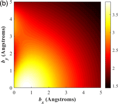
The electrodynamic theory outlined previously for a semi-infinite slab is used to analyze surface core hole screening in MgO cubes. Strictly speaking, there will be some error in modeling a cube as a semi-infinite slab. For the ~8–9 nm surface loss decay length, as much as ~20% of a 81.5 nm cube is affected by the electron beam entrance and exit surfaces, which is nevertheless not accounted for in our simple model. The cube corners are less important, since from Figure 3d the low-loss spectrum for the corner is similar to the bulk spectrum. Figure 5a shows the O K-edge energy gain spectrum for a STEM probe incident along an end-on MgO free surface. The energy gain was calculated using equation (14), assuming s = 0 and the experimental illumination and measurement parameters used in this study. The maximum energy gain is slightly higher than in the bulk (i.e., 3.9 versus 3.7 eV), and the surface energy gain spectrum shows more structure compared with its bulk counterpart (Fig. 4c). For example, there is a small peak in the surface energy gain spectrum at 2.7 eV. Figure 5b plots the energy gain as a function of impact parameter (b x, b y), with b x = 0 corresponding to an atom at the free surface. In an isotropic bulk material, the energy gain has a radial dependence with respect to the impact parameter magnitude, but for a free surface, the spatial dependence is more complicated, which leads to the extra structure observed in the surface energy gain spectrum.

Fig. 5. (a) Calculated O K-edge energy gain spectrum for a STEM probe incident along an end-on free surface in MgO. (b) The energy gain as a function of impact parameter, with b x = 0 corresponding to atoms at the free surface. In (c), the dynamic screening contribution to the energy gain is plotted as a function of energy for bulk and free surface configurations. The simulations assume a 200 kV, diffraction limited STEM probe with 7.2 mrad semi-convergence angle and zero defocus. The EELS collection semi-angle is 7.2 mrad. (d) The measured right cube face O K-edge and corresponding fully screened spectrum. The area under the graph is normalized for a direct comparison. The fully screened spectra for the bulk and surface configurations are superimposed in (e), with the maximum intensity normalized.
In Figure 5c, the dynamic screening contribution to the surface energy gain [i.e., second term in equation (14)] is plotted as a function of energy loss  $\hbar \omega$ for the impact parameter b x = 0.75 Å, b y = 0 Å (from Fig. 5b, the energy gain for this impact parameter is close to the maximum value). The interested reader is referred to Mendis & Ramasse (Reference Mendis and Ramasse2021) for more details on the physical mechanisms underpinning dynamic screening. From Figure 5c, it is clear that surface loss plasmons are the dominant mechanisms in dynamic screening. However, static screening [i.e., first term in equation (14)] contributes an energy gain of 2.6 eV, while the total dynamic contribution is only 1.3 eV. Figure 5c also shows the dynamic contribution to the bulk energy gain, calculated using equation (13) in Mendis & Ramasse (Reference Mendis and Ramasse2021) for zero impact parameter (i.e., maximum energy gain in the bulk). The energy gain contribution is much larger than the surface and is primarily due to the bulk plasmon mode at 22.6 eV, with lower energy-loss interband scattering also making a contribution. Static screening contributes 1.8 eV to the overall energy gain in the bulk, while the total dynamic contribution is 1.9 eV. The relative importance of static versus dynamic screening is, therefore, dependent on the specimen geometry (i.e., bulk or free surface).
The surface energy gain spectrum in Figure 5a was deconvolved from the experimental O K-edge extracted from the right face of the MgO cube (Fig. 4a). The experimental spectrum had to be binned once to minimize significant noise being introduced during deconvolution (the effective dispersion is, therefore, decreased to 0.4 eV/channel). Figure 5d shows the resulting “fully screened” spectrum for the surface, which in Figure 5e is compared with the fully screened spectrum for the bulk material, extracted from Figure 4d. Despite the difference in measured EELS edge shapes, the calculated fully screened spectra for surface and bulk look very similar, with the former showing slightly higher intensity at the edge onset, which may be due to genuine surface states and/or errors in the modeling of the energy gain spectra, particularly for the free surface. It should also be noted that due to the range of impact parameters the “surface” fully screened spectrum comprises of both surface and interior “bulk” oxygen atoms, and therefore, the overall surface state contribution will be weaker compared with surface atoms only. Figure 5e is testimony to the fact that a reproducible ground state spectrum can be extracted from vastly different sample scattering geometries, even though the measured EELS spectra are different. The ground state, fully screened spectrum has the advantage of being easier to simulate using electronic structure methods, since it is free from core hole effects. There are also implications for electronic state measurements at surfaces and/or interfaces using EELS. The extra intensity at the EELS edge onset is only partly due to genuine surface or interface states. For an accurate description surface or interface core hole screening must also be taken into account, particularly if the material is an insulator.
Mg L3,2-Edge Surface Core Hole Fine Structure
The low-loss spectrum image in Figure 2b was used to extract the Mg L3,2-edge from the “bulk” region, as well as the left and right cube faces. The EELS edges are shown superimposed in Figure 6a; there is a hint of extra intensity at the edge onset for the cube face spectra, although a better signal-to-noise ratio is required to make more conclusive statements. Surface states in a MgO single crystal have previously been reported at the Mg L3,2-edge onset using reflection EELS measurements, although the weak fine structure was only revealed by differentiating the energy loss spectrum (Henrich et al., Reference Henrich, Dresselhaus and Zeiger1976). In bulk MgO, the Mg L3,2-edge onset consists of spin–orbit split, core hole excitons, due to promotion of 2p shell electrons with j = 3/2 and 1/2 quantum number into unoccupied states (O'Brien et al., Reference O'Brien, Jia, Dong, Callcott, Rubensson, Mueller and Ederer1991).

Fig. 6. (a) Experimental Mg L3,2-edges extracted from the interior (“bulk”) as well as left and right faces of the MgO cube shown in Figure 2a. The simulated Mg L3,2-edge impact parameter distribution P(b) is shown in (b), while (c) is the energy gain spectrum calculated for bulk MgO. The simulations assume a 200 kV, diffraction limited STEM probe with 7.2 mrad semi-convergence angle and zero defocus. The EELS collection semi-angle is 7.2 mrad. In (d), the measured “bulk” and corresponding fully screened spectra are shown superimposed. The area under the graph is normalized for a direct comparison. The calculated Mg L3,2- energy gain spectrum for a STEM probe incident along an end-on free surface is plotted in (e), while (f) shows the experimental right cube face Mg L3,2-edge and corresponding fully screened spectrum (the area under each graph is normalized). The bulk and surface fully screened spectra are superimposed in (g), with maximum intensity normalized.
Electrodynamic theory can be used to obtain a fully screened spectrum that is largely free of any core hole effects. Figure 6b shows the Mg L3,2-edge impact parameter distribution, P(b), for the experimental conditions used in this study. Due to the smaller energy loss (i.e., ~51 eV edge onset), the inelastic scattering is more delocalized, and the P(b) curve shows a distinct “volcano” profile at small impact parameters (Cosgriff et al., Reference Cosgriff, Oxley, Allen and Pennycook2005). This is because more localized scattering events give rise to larger scattering angles, which lie outside the EELS spectrometer entrance aperture. The Mg L3,2-energy gain spectrum for bulk MgO is shown in Figure 6c and consists of a single peak with narrow energy distribution (<0.05 eV). The gain spectrum is, therefore, similar in shape to a Dirac delta function, centered on the maximum energy gain value of 0.36 eV. The maximum energy gain for Mg L3,2 is much smaller than that for the O K-edge (see Fig. 4c), since the large delocalization in both impact parameter and  $z_0\sim ( {v\hbar /{\rm \Delta }E} )$ for the former gives rise to only a small Coulomb interaction. Deconvolution of the energy gain from the EELS measurement yields a fully screened spectrum that is energy shifted, without any significant changes to the edge shape (Fig. 6d). This behavior is consistent with approximating the energy gain spectrum to a delta function. The Mg L3,2-energy gain spectrum for a STEM probe incident along an end-on free surface is shown in Figure 6e. The maximum energy gain (i.e., 0.44 eV) is slightly higher compared with the bulk, although still sufficiently small to cause only minor changes to the fully screened surface spectrum (Fig. 6f). Any surface core hole effects are, therefore, harder to detect in the Mg L3,2-edge, due to the stronger delocalization for this energy loss. This should be compared with the higher energy O K-edge, where the more localized scattering makes it easier to probe surface-specific information. Finally, Figure 6g compares the fully screened spectra for bulk and surface geometries. The two spectra show only minor differences, consistent with the fact that they represent the ground state electronic structure.
Conclusion
The core hole interaction in the vicinity of a free surface is modeled using electrodynamic theory. Due to Maxwell's boundary conditions for the electric field, core hole screening near a free surface is different from bulk screening. The electrodynamic model calculates the energy gain required to separate the negatively charged incident electron from the positively charged core hole. The STEM illumination and EELS collection geometries give rise to a range of impact parameters, each with its own energy gain value. This results in an energy gain spectrum that can be deconvolved from the EELS measurement to give a “fully screened” spectrum that is, in principle, free from core hole effects. Since the fully screened spectrum represents the ground state of the solid, it is easier to simulate using electronic structure methods.
In this work, the surface core hole interaction is investigated for the O K- and Mg L3,2-edges in MgO cubes. The cube shape enables measuring free surface EELS spectra using STEM. Compared with bulk the O K-edge for the cube faces showed extra intensity, in the form of a “shoulder” at the edge onset. The O K-surface energy gain spectrum, calculated using the electrodynamic model, revealed more structure and slightly higher energy gains compared with the bulk material. Furthermore, static screening was found to be more important than dynamic screening contributions from surface plasmon modes. This contrasts with screening behavior in bulk MgO, where both static and dynamic screening from the bulk plasmon and interband transitions are equally important. It is found that the fully screened spectra for both “bulk” and cube face O K-edges in MgO are very similar, demonstrating a key benefit of the electrodynamic method, namely extracting data that is more representative of the ground state. In contrast to the oxygen signal, the Mg L3,2-edge showed very little difference in fine structure between bulk and cube face spectra. This is likely due to the large delocalization in inelastic scattering for the low energy loss Mg L3,2-edge, which results in a measurement that is less surface sensitive. The results in this paper have wider implications for (say) high spatial resolution measurement of EELS edges at interfaces between two different materials. An accurate analysis of the data must include the correct screening of the core hole at the interface. The electrodynamic theory outlined here can easily be extended to an interface between two different materials. It provides a computationally efficient method to model screening and also remove core hole effects from the fine structure.
Supplementary material
To view supplementary material for this article, please visit https://doi.org/10.1017/S1431927621012691.
Acknowledgement
BGM is grateful to Dr Pavel Potapov for his ‘temDM’ open-source plugin for principal component analysis (http://temdm.com).
Financial support
This work was financially supported by the North East Centre for Energy Materials (NECEM) and EPSRC, UK (Grant No. EP/R021503/1).


 Open access