Introduction
EL is the major characterization technique for LEDs probing the active region of the whole device under operation. However, as an usually integral measurement it averages over the whole LED. An even deeper insight can be obtained employing spatially and spectrally resolved EL (µ-EL). This technique is used to gain valuable insights into GaN-based LEDs. It is a non-destructive and fast method which provides information about the full device including epitaxial growth and processing. The resulting EL data yield full spectra at each point of investigation at a 1 µm resolution. The recorded data set allows to extract the distribution of the peak wavelength, the intensity, the linewidth and the presence of other recombination paths (DAP, non-radiative, etc. ). Those data can be correlated with a conventional microscope image to compare morphology and defects from growth and/or processing with the EL distribution. Furthermore, EL features such as peak wavelength and intensity are depending on local device temperature and current injection, respectively. The disclosed device properties might be used to improve spatial and spectral emission characteristics of LEDs. Within the present work EL-homogeneities, In-fluctuations, heat generation due to ohmic losses, current injection homogeneity, and transparent contacts are investigated.
Experimental
InGaN/GaN-LEDs emitting near the UV are grown by low pressure MOVPE in a horizontal reactor (AIXTRON AIX 200 RF) on c-plane sapphire substrates. The structure consists of 2000 nm GaN and 1000 nm Si-doped GaN followed by the active region, a 100 nm Mg-doped Al0.08Ga0.92N layer, and finally 300 nm p-doped GaN. The active region containes either a 50 nm thick In0.09Ga0.91N-layer (double heterostructure) or 3 periods of In0.09Ga0.91N/GaN (MQW structure). Conventional photolithography is used to define the mesa structure. Chemically-assisted ion-beam etching (CAIBE) transferred the pattern using a conventional photoresist mask. A second lithographic step defines the n- and p-contact area, using lift-off technique and subsequent Ni/Au metallization for ohmic contact formation. The resulting LEDs reveal narrow dominating peak emission at about 400−410 nm. The devices have series resistances of approximatly 30 Ω.
The spatially resolved µ-EL system is based on an optical microscope using UV-transparent lenses with a long working distance and computer controlled scanning stages. A DC-motor driven scanning stage enables the scanning with a resolution of 250 nm. The µ-EL is spatially resolved detected. For µ-EL an overall spatial resolution of 1 µm is obtained. The electroluminescence is dispersed in a 0.5 m spectrometer and detected by a liquid nitrogen cooled Si-CCD camera. The spectral resolution for µ-EL measurements reported here is 0.5 nm. All µ-EL measurements are performed at room temperature. LEDs are investigated from both the p-contact- and substrate-side (hereafter called front- and backside). A complete spectrum is recorded at each pixel (x,y) and stored during the scanning over 128 × 100 pixels. Typical examples of extracted information are local EL spot spectra, EL wavelength images in a certain window, i.e. mappings of the local emission peak wavelength, as well as sets of EL intensity images. For the µ-EL measurements also cf. [Reference Fischer, Christen, Zacharias, Schwegler, Kirchner and Kamp1].
Results and Discussion
Figure 1 shows the comparison of a DH and MQW LED,revealing a major difference in the epitaxial quality of the active region and the subsequently grown p-AlGaN barrier layer. Figures 1a-f correspond to an imperfect DH-LED, whereas Figures 1g-l show results obtained from an improved MQW-LED. The micrographs of both circular LEDs are given in Figure 1a and 1g, showing the inner, non-transparent p-contact with the bondwire and the surrounding n-contact metallization. The integral EL spectra are given in Figures 1b and 1h. The DH-LED with the insufficient active region reveals a double peak EL where the emission at 400 nm is from the InGaN-layer and the EL at 440 nm originates from recombination within the p-GaN layer. Figure 1c shows the spatial distribution of the EL intensity from the InGaN (λ = 380−420 nm), whereas Figure 1d maps the emission intensity at about 440 nm (p-GaN) which is signifcantly more homogenously distributed. The peak emisson wavelength distribution is depicted in Figure 1e and 1f. Again the lower wavelength emission is more homogeneously distributed. The InGaN related emission (Figure 1e) reveals a certain inhomogeneity over the device. The observed wavelengths correspond to In-contents between 6−9%, using a bowing parameter of 3.2 eV. Since In-fluctuations are present but only of minor significance, the device is most severly limited by the inhomogenous intensity of the InGaN/GaN EL as can be seen from Figure 1c.
Once the quality of the InGaN/AlGaN active region is improved single peak emission is obtained (Fig. 1h). Figures 1i and 1j show the measured EL at current densities of 27 and 318 A/s, respectively. For the lower current densities the µ-EL reveals a uniform distribution of the EL intensity (1i) and the wavelength (1k). For higher current densities a localization of highest intensity at the mesa area takes place (Figure 1j). Low In fluctuations from 0.09 to 0.11 are found evidencing the good chemical uniformity of the InGaN layer (Figure 1l).

Figure 1 Micrographs (1a, 1g) and integral EL spectra (1b, 1h) of imperfect and improved LEDs, respectively. EL intensity distributions (1c, 1d, 1i and 1j) and wavelength distributions (1e, 1f, 1k and 1l) reveal strong differences between the LEDs related to the epitaxial quality.
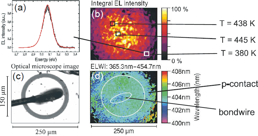
Spatial temperature distributions can be derived from µ-EL by fits to the spatially resolved spectra [Reference Zolina, Kudryashov, Turkin and Yunovich2]. Figure 2 shows this examplarily at three points taken from the backside of the MQW-LED. The impact of such a temperature distribution can be seen at the wavelength image in Figure 2. A redshift beneath the p-contact due to increased temperature by elevated current density is observable. Heat drain effects of the bondwire can also be identified. For a more extended discussion of temperature distributions in InGaN MQW-LEDs cf. [Reference Schwegler, Seyboth, Schad, Scherer, Kirchner, Kamp, Stempfle, Limmer and Sauer3].

Figure 2 EL intensity distribution at j=320 A/cm−2 (2b) and local temperatures derived using spectral fits to local spectra (2a). The EL wavelength distribution (2d) reveals the highest temperature (longest wavelength) beneath the p-contact.The bondwire (2c) acts as heat drain as can be seen from shorter wavelengths.
Transparent contacts are employed in LED technology to combine homogeneous current injection with good outcoupling efficiency. Therefore the contact geometry has to achieve homogeneous current injection with lowly absorbing materials. Figure 3 shows a transparent contact (Ni/Au 2 nm/6 nm) on the p-GaN of a LED. Although the spatial distribution of wavelength maxima seems quite homogeneous, the integral intensity distribution reveals a strongly increased EL-intensity at the mesa edge next to the n-contact which is also clearly visible in the intensity linescan. This can be explained by the different resistances of metal layer and n-GaN leading to a current flow pattern minimizing the overall resistance of the device. An additional high-resistivity undoped GaN layer between the active layer and the contact layer should spread the current more uniformly [Reference Mukai, Takekawa and Nakamura4].

Figure 3 LED with transparent contact (including grid-shaped contact-enforcement) showing inhomogeneous brightness due to inhomogeneous current injection.
Conclusions
InGaN/GaN-LEDs have been comprehensively characterized by spatially resolved µ-EL. The non-destructive µ-EL probes the relevant properties of the optically active region of the devices under operation. It reveals all deficiencies from either epitaxial growth or processing and is found to be a very powerful technique to analyze LEDs. µ-EL provides direct access to emission from the InGaN active region as well as from the p-GaN. These data have an extremely high relevance since they are obtained from the optically active region of the device under operation. Device properties like current injection and heating can be disclosed enabling an improved device design.
Acknowledgements
Financial support by German Ministry of Science and Education (BMBF) and Osram Opto Semiconductors under contract No. 01 BS 802 is gratefully acknowledged by the group at Ulm University. The group at Magdeburg University acknowledges financial support by the Kultusministerium of Sachsen-Anhalt under contract No. 1432A/8386B.