


Introduction
Quantitative nanoscale chemical imaging of elements present in low concentrations is required in many areas of scientific research. The chemical, physical, and electronic properties of materials can be dramatically changed by additions of even small concentrations of doping or alloying elements. For example, dopants are used in semiconductor materials to tune their electronic properties.[Reference Erwin, Zu, Haftel, Efros, Kennedy and Norris1] Likewise, small additions of carbon (C) or boron (B) in steel are known to drastically change their mechanical properties.[Reference Taylor, Fourlaris and Clough2] Modern materials are often designed with low concentrations of elements with complex nanoscale structural features to improve their performance. To establish the link between macroscale properties and the local chemical characteristics, quantitative nanoscale mapping of trace concentrations of elements is essential.
Secondary ion mass spectrometry (SIMS) is a well-known high-sensitivity chemical analysis technique widely used for the investigation of chemical composition even down to ppm levels of concentration.[Reference Benninghoven, Rüdenauer and Werner3,Reference Kumar, Pfeffer, Willsch, Eibl, Yedra, Eswara, Audinot and Wirtz4] However, the quantification of SIMS intensities is not straightforward mainly because of the strong variations in ionization yield for a given element as a function of the matrix elements (i.e., matrix effect). Another limitation of SIMS is the lateral resolution which is fundamentally limited by the ion–solid interaction volume size of ~10 nm. To overcome this limitation, a correlative microscopy approach is often employed.[Reference Wirtz, Philipp, Audinot, Dowsett and Eswara5,Reference Yedra, Eswara, Dowsett and Wirtz6] In this context, it should be noted that atom probe tomography[Reference Kelly and Miller7] (APT) can provide quantitative high-resolution and high-sensitivity imaging of the elements, but the main limitations of this technique are that the sample preparation is very laborious and, more importantly, the analysis volume is extremely small (~100 nm needles with tip radius of <10 nm and volume in the 104–107 nm3 range). Hence, in contrast to SIMS, the analysis of fields of view (FOV) in the micrometer length scales is not possible with the APT technique.
A well-known method often used in the quantification of SIMS depth profiles (i.e., 1D analysis) is by using reference samples of known concentrations obtained by ion implantation or by a dedicated preparation of special sets of samples containing the known concentration of elements distributed uniformly. The latter method has been successfully used in the past also to quantify SIMS images[Reference Valle, Drillet, Bouaziz and Migeon8,Reference Arlazarov, Gouné, Bouaziz and Hazotte9] (i.e., 2D analysis) in multiphase steels. Carbon contents were determined from a calibration curve established from dual-phase steels with known concentrations of carbon. The main limitation of that approach is that dedicated sets of special reference samples are needed to obtain the calibration curve and only few discrete points in the concentration space are covered.
In the present work, we introduce a new method for direct quantitative SIMS imaging based on cross-sectional imaging of ion-implanted reference samples prepared using optimal ion dose and implantation energy. The main advantage of this new approach is that within a single image acquisition, reference concentrations varying continuously over few orders of magnitude can be determined. This conversion can then be applied to other samples with the same matrix as the reference sample. We demonstrate this method with an application example in the analysis of dopant concentrations in carrier-selective passivating contacts used in c-Si solar cells.[Reference Nogay, Ingenito, Rucavado, Jeangros, Stuckelberger, Wyss, Morales-Masis, Haug, Loper and Ballif10,Reference Python, Dominé, Söderström, Meillaud and Ballif11] A method commonly used in the solar cell industry to assess dopant profiles is electrochemical capacitance voltage profiling. However, this technique reflects only the active dopant concentration and not their total concentration, and since it is a 1D method, it does not reveal local variations. We apply the new method for quantitative nanoscale SIMS imaging to the laterally inhomogeneous dopant distribution across the deposited layers and the in-diffused region of a passivating contact in a photovoltaic material with surface texture in order to better understand its macroscopic electronic properties. The method can also be broadly applied to other areas of research.
Experimental methods
Reference samples
A 4″ silicon (Si) wafer with a crystal orientation ⟨100⟩ was implanted with B with implantation energy of 190 keV and a dose of 1016 ions/cm2 at the Surrey Ion Beam Centre, Guildford, UK. The specified dose accuracy from the measurements is better than 1% in both uniformity and the absolute value. The implantation was performed over the full 4″ wafer, apart from an approximate exclusion zone of around 3 mm all around the edge of the wafer where it is held in place during the irradiation. The irradiation took place at 7° off axis with a 22° twist to avoid channeling down the ⟨100⟩ direction. The energy of implantation was chosen such that the concentration maximum forms as deep as possible from the surface and to have an extended concentration profile. This is necessary to have a sufficient number of data points (i.e., pixels) across the concentration profile during the subsequent cross-sectional SIMS imaging. A Monte Carlo-based simulation program, SRIM (Version 2013),[Reference Ziegler, Ziegler and Biersack12] was used to estimate the concentration profile as a function of the depth. The maximum concentration of B according to the simulation is 5 × 10²⁰ at./cm3 (or 1 at.%) at a depth of 550 nm from the surface. In addition, SDTRIMSP code[Reference Mutzke, Schneider, Eckstein and Dohmen13] was used to simulate B implantation into Si. Further details of the simulations are provided in Supplementary Material.
Passivating contact samples for solar cells
The test structures for passivating solar cell contacts were fabricated on symmetrically processed p-type float zone Si wafers with [100] crystal orientation. After KOH texturing and cleaning, a thin (~1 nm) SiOx chemical oxide was grown by wet chemical oxidation of the substrate in hot nitric acid. Subsequently, a 30-nm thick layer of boron-doped SiCx~5at.% was deposited by parallel-plate plasma-enhanced chemical vapour deposition. The deposition was done on both sides such that the layers are symmetrically deposited on the Si substrate. The boron diffusion was then obtained by annealing the sample at 850 °C in a quartz tube furnace under inert gas atmosphere without dwell time at peak temperature. Thereafter, the sample was covered on both sides with a SiNx:H layer which serves as a hydrogen donor. Hydrogen is released from this layer by annealing at 450 °C on a hot plate. Eventually, the SiNx layer was removed in hydrofluoric acid (HF). The process is described elsewhere in detail.[Reference Nogay, Ingenito, Rucavado, Jeangros, Stuckelberger, Wyss, Morales-Masis, Haug, Loper and Ballif10,Reference Nogay, Stuckelberger, Wyss, Rucavado, Allebé, Koida, Morales-Masis, Despeisse, Haug, Löper and Ballif14] A schematic of the final stacking of the layers on the textured Si is shown in the Results section (Fig. 2(a)).
For SIMS 2D imaging, the cross-section of the ion-implanted reference sample as well as of the textured solar cell sample was prepared as follows. First, the samples were cleaved and then the cross-sections were exposed by sandwiching two pieces of the same type face-to-face using an epoxy glue. After curing for 24 h, the entire sandwich assemblies were embedded into larger epoxy discs. The embedded cross-sectional samples were then mechanically polished to mirror finish. For transmission electron microscopy (TEM), the cross-sectional sample of the textured solar cell sample was prepared by conventional focused ion beam (FIB) preparation in the form of H-bar.[Reference Hull15]
SIMS analyses were performed in 1D (i.e., depth profiling) mode as well as 2D (i.e., imaging) mode. SIMS depth profiling was done using a Cameca SC-Ultra with O2+ primary ions with a primary energy and current of 7 keV and 85 nA, respectively. For these conditions, the SIMS depth resolution is estimated[Reference Wilson, Stevie and Magee16] to be ~10 nm and an estimated slope of ~20 nm per decade. The depth was calibrated by measuring the crater depth using a KLA-Tencor P17 profilometer. For SIMS imaging, a Cameca NanoSIMS50 instrument with an O− primary ion beam with an impact energy of 16 keV was used. The probe current was 12 pA and the probe size was estimated to be 400 nm. The SIMS images of 11B+, 12C+, and 28Si+ were obtained simultaneously in matrices of 256 × 256 pixels. The dwell time was 10 and 20 ms per pixel for FOV of 10 × 10 and 40 × 40 µm2, respectively. Mass resolving power was set to 3000. The cross-sectional reference sample and the solar cell sample were imaged consecutively at exactly identical conditions. Before the acquisition of SIMS images, the area of interest is irradiated with primary ions to clean the surface. This is a standard procedure to remove possible surface modification due to exposure to air during sample transfer. Furthermore, as the primary ions were O−, a steady-state oxygen concentration in the matrix is reached resulting in enhanced ionization yields.
An FEI Tecnai G2 F20 TEM operating at 200 keV was used for imaging in the scanning TEM (STEM) mode, and the high-angle annular dark field (HAADF) images were recorded using a Fischione Model 3000 HAADF detector. Scanning electron microscopic (SEM) images were acquired in a secondary electron (SE) mode in an FEI Scios operating with a 10 keV primary electron energy.
Results and discussion
The central idea of the SIMS image quantification method presented here is based on the comparison of intensity profile across a sample of known concentration profile with the intensities in a sample of unknown concentration. Figure 1(a) shows a cross-sectional SIMS image from the ion-implanted reference sample. Figure 1(b) shows the B-depth profile (in blue) in Si quantified using the ion implantation parameters described earlier. The quantity of boron implanted in silicon is known (1016 at./cm2), and it corresponds to the integrated signal below the curve B/Si over the depth of implantation. This is the common method used to correlate B intensity to concentration.[Reference Wilson, Stevie and Magee16]
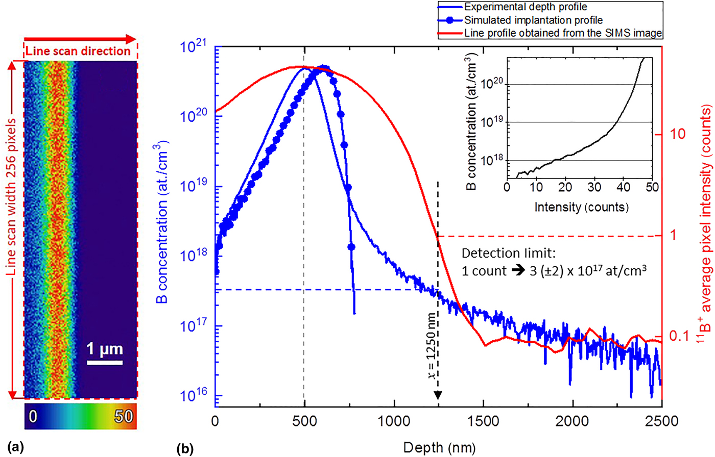
Figure 1. (a) Cross-sectional 11B+ SIMS image of the ion-implanted reference sample, (b) boron distribution obtained by depth profiling (blue curve), simulated implantation profile (blue curve with dots), and a line scan intensity profile across the cross-section SIMS image (red curve). The line scan direction and the integration width used for averaging are indicated in (a). For the acquisition conditions here, the detection limit (an average of 1 count per voxel) for the imaging SIMS is found to be ~3 (±2) × 1017 at./cm3 with a pixel size of 39 nm. The nonlinear relationship between the intensity and the concentration is shown in the inset as a semi-log plot.
An intensity profile (in red) measured from the SIMS cross-section image is superposed together with the depth profile in Fig. 1(b). The results indicate a maximum B concentration of 4.8 × 10²⁰ at./cm3 at a depth of ~500 nm. The direction of the intensity profile as well as the integration width are indicated in Fig. 1(a). For comparison, the simulated implantation profile is also shown in Fig. 1(b), and a good agreement between experimental and simulated data is observed. The maximum value of concentration determined from simulation (~5 × 10²⁰ at./cm3) agrees well with the experimentally determined concentration. There is, however, a minor offset in the peak positions of ~100 nm. This discrepancy could be attributed to both computational (e.g., parameters used for SDTRIMSP which was set to reproduce TRIM, i.e. Transport of ions in matter data) and experimental (e.g., calibration) errors. On the leading edge, the experimental depth profile and the simulated implantation profile agree well. The difference in the trailing edge between experimental depth profile and simulated data is at least partially due to the atomic intermixing and the possible presence of irradiation-induced diffusion during depth profiling with the ${\rm O}_{\rm 2}^{\rm +}$ beam. In comparison, the simulated data show only the implantation profile and does not capture these processes which occur during depth profiling.
With the help of the superposed curves in Fig. 1(b), the 11B+ intensity can be calibrated to B concentration as shown in the inset. Doing so, a nonlinear correlation between the intensity and the concentration is observed within a single sample. The standard method of the quantification of SIMS depth profiles assumes a linear approximation for the relationship between the intensity and the concentration. Interestingly, when we correlate the NanoSIMS line profiles and the concentration, the relationship is found to be nonlinear. We do not believe that this is linked to the averaging effect of the probe size as that would only smoothen rather than accentuate a nonlinear relationship. The results suggest a nonlinear relationship between the intensity and the concentration in the investigated concentrated range. From the plots shown in Fig. 1(b), we also note that the line scan intensity from the SIMS image reaches 1 count per voxel (at x = 1.25 µm) and the concentration at that point ~3 (±2) × 1017 at./cm3, which quantifies the detection limit (defined here as the concentration corresponding to an average intensity of 1 count per voxel) for a pixel-size of 39 nm and the applied SIMS imaging conditions. Further considerations in the determination of detection limit are discussed in Supplementary Material.
It is worth noting that the intensity profile will be a convolution of the actual concentration profile C (ignoring matrix effect, etc.) and the Gaussian probe profile (P). Hence, intensity I = C * P. Mathematically, a deconvolution of the probe profile from the experimental line profile would be expected to “sharpen” the profile by eliminating Gaussian broadening. In practice, however, it works only when the input profiles are smooth such that a finite Fourier series expansion is sufficiently accurate, and more importantly, the high-frequency noise background gets amplified during deconvolution. For a robust and reliable deconvolution, the actual beam profile characteristics (such as Gaussian vs. Lorentzian and optical aberrations) will be needed, and the experimental data should not be noisy. Experimentally, a smaller probe size and a wider B-rich zone (e.g., higher implantation energies) would help to mitigate the effects of probe size on the intensity profiles.
SIMS quantification in depth profiling mode is often done by taking the ratio of the intensity of minor element to major element such as B/Si. This normalization step is done to eliminate variations in B intensity due to factors other than real variation in concentration. This approach has the limitation that intensities should be sufficiently high (>103 counts per second) to suppress Poisson noise, and it also assumes that the concentration of the major element is essentially invariant. The normalization of B/Si is a standard approach in depth profiling wherein the signal is averaged over the whole FOV. The same approach cannot be directly applied for quantitative SIMS imaging, the main reason being that a SIMS image may contain two or more types of materials with completely different chemical compositions within the FOV. When a material, which does not contain Si, is present together with another material containing Si, the division of B by Si will result in division by 0 resulting in completely meaningless pixel values. Likewise, Si may not be a major element across the full FOV of the SIMS image. In such cases, the division of B by Si will introduce artifacts. Furthermore, the noise in Poisson statistics is given by $\sqrt N$ , where N is the pixel intensity. Thus, the signal intensities of dopants are noisier in an imaging mode than in the case of depth profiling. Hence, small fluctuations in the intensity will be artificially amplified by taking the B/Si normalization method. For these reasons, we do not apply this method to quantify SIMS images. To improve the signal-to-noise ratio in individual pixels, in the present approach, the line profile in Fig. 1(b) is integrated over the full image width of 256 pixels. An even level of Si intensity is taken as an indication of the absence of spurious fluctuations in primary ion current and other parameters affecting 11B+ signal intensity. Thus, the 11B+ intensity is directly calibrated to the B concentration as shown in the inset of Fig. 1(b).
In this context, it should be noted that there is a well-known inverse relationship between resolution and the physically possible lowest measurable concentration.[Reference Wirtz, Philipp, Audinot, Dowsett and Eswara5] Briefly, when the voxel gets smaller (i.e., higher resolution), the number of atoms it can physically contain also get smaller thereby limiting the lowest theoretically detectable concentration. This fundamental link between resolution and the lowest concentration sets a physical limit. The results shown in Fig. 1(a) also allow us to compare the experimental detection limit with the theoretical limit based on the voxel dimensions of the SIMS image. The individual pixel size in the SIMS image shown in Fig. 1(a) is 39 nm, and the image was obtained by summing four planes of images.
The primary current was 12 pA, the probe size was ~400 nm, the pixel array was 256 × 256, the dwell time was 10 ms/pixel, and the secondary ion intensities were summed over four planes for the image shown in Fig. 1(a). So, the total dose was 1.9 × 10¹⁷ ions/cm2 or ~3 × 10⁶ ions/pixel. The sputtering yield of 16 keV oxygen primary ions in the Si sample was calculated to be 0.8 at./ion by SRIM simulation. Hence, the total number of atoms sputtered per voxel is ~2.4 × 10⁶ atoms. Taking the density of Si as 5 × 10²² at./cm3, it can be shown that the estimated voxel size is about 39 × 39 × 30 nm3. The lowest possible dopant concentration that is theoretically possible is 1 dopant atom of the 2.4 × 10⁶ atoms or ~2 × 10¹⁶ at./cm3 or 0.4 ppm. The difference between this theoretical limit and the experimentally measured detection limit of 3 (±2) × 1017 at./cm3 is attributed to the limited useful yield resulting mainly from losses associated with ionization efficiency and the transmission of the spectrometer. In the present case, a detection limit of 3 × 10¹⁷ at./cm3 would mean 15 B atoms per voxel to detect 1 B+ count. This corresponds to a useful yield of 6.7 × 10⁻². For comparison, Migeon et al.[Reference Migeon, Saldi, Gao and Schuhmacher17] reported a useful yield of 3.1 × 10⁻³ for the detection of B (as B+) in Si using O2+ primary ions. The difference in useful yields is mainly because of the intrinsic differences in the transmission of the instruments and possible differences in analysis parameters such as mass resolution.
As an application example of this quantitative SIMS imaging method, carrier-selective passivating contacts on a textured c-Si wafer were analyzed by correlatively combining TEM and SIMS imaging. A schematic cross-section of the solar cell sample is shown in Fig. 2(a). As can be seen, the surface of textured c-Si substrate is passivated with a thin layer of SiOx (~1 nm) and an amorphous hydrogenated boron-doped SiCx layer (~30 nm). The presence of carbon in the SiCx layer enables to (i) tune the optical properties of the layer, (ii) improve the resilience of the layer to blistering due to hydrogen effusion occurring during subsequent annealing steps, and (iii) enhance its stability to wet chemistry processes used during the solar cell fabrication procedure.[Reference Nogay, Ingenito, Rucavado, Jeangros, Stuckelberger, Wyss, Morales-Masis, Haug, Loper and Ballif10] The diffusion of dopants from the SiCx layer to the c-Si wafer during the annealing step contributes to a reduction of charge carrier recombination at the contact. The SiCx layer is strongly doped with boron in order to provide hole-selectivity, establish good contact to the external metallization, and to act as a dopant source for diffusion through the interfacial oxide and into underlying c-Si wafer.
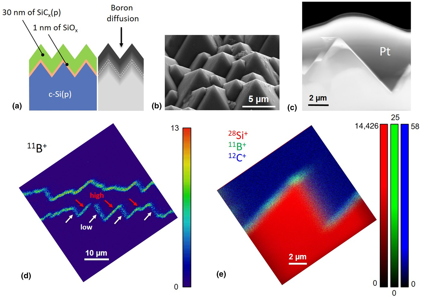
Figure 2. (a) Schematic view of the multilayer solar cell stack and an illustration of B diffusion, (b) SEM image obtained in the SE mode of the textured solar cell sample surface, (c) cross-sectional STEM–HAADF image, and (d and e) cross-sectional SIMS images with different FOVs. The secondary ion intensities are given by the colour bars. The arrows in (d) indicate the edges with higher intensities (in red) and lower intensities (in white). This effect is attributed to the geometric orientation of the facets as discussed in Fig. 3.
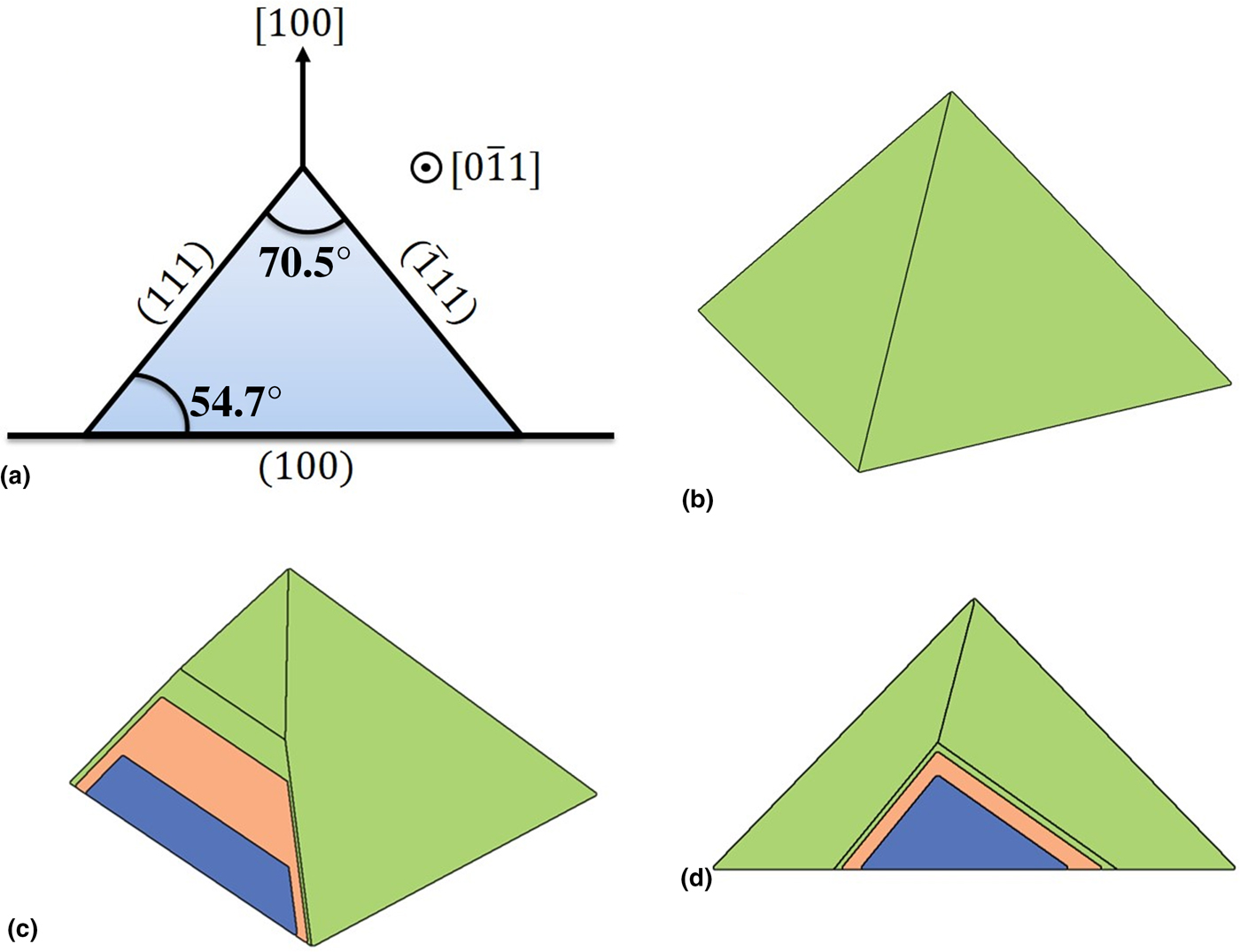
Figure 3. (a) Schematic of the crystallographic relationships in the cross-section of pyramid as seen along the <011> direction and (b–d) 3D models of multilayer pyramid structure to illustrate the geometric effect of the slicing angle on the apparent enlargement of layer thickness. The colours indicate different layers as labeled in Fig. 2(a).
A sample annealed at 850 °C was used for the present study. An SE image of the textured wafer surface of the sample is shown in Fig. 2(b). The (111) facets of the pyramids exposed after the texture etch are clearly visible. To evaluate the cross-sectional features, a STEM–HAADF image of a cross-section of a typical pyramid is shown in Fig. 2(c). The Pt layer was deposited during the FIB preparation to protect the surface from ion beam damage during the sample preparation. The SIMS images of the cross-section sample are shown in Figs. 2(d) and 2(e). Figure 2(e) was acquired at exactly the same conditions as Fig. 1(a) such that the boron concentration in the c-Si substrate can be quantified from the secondary ion intensity using the calibration curve shown in the inset of Fig. 1(b).
Before evaluating the dopant concentrations, it is necessary to consider the crystallographic and geometric aspects of the pyramids in textured Si. The facets of the pyramids are (111) type which are formed on the [100] oriented Si wafer. A schematic illustration of the angular relationships between the facets and the substrate in a cross-section viewed along the ⟨011⟩ axis is shown in Fig. 3(a). The well-defined angular relationships allow assessing concentration variations of dopants along different crystal directions. However, the pyramid has to be precisely oriented at the time of sample preparation to subsequently determine the concentration variation along different crystallographic directions. This is a more elaborate investigation for future work and beyond the scope of the present study. Another aspect associated with the geometry of the pyramids is the influence of cutting angle on the apparent layer thicknesses as shown in Figs. 3(b)–3(d). The cutting plane results in dramatically different apparent layer thicknesses according to its angular relationship with individual facets locally. Note that the total thickness of the passivation layers in the analyzed sample is ~30 nm as shown schematically in Fig. 2(a). However, the pixel size in Fig. 2(e) is 39 nm, i.e., the entire multilayer stack is smaller than a single pixel in the image. However, we see the boron-containing layer to be extended over nearly 1 µm in Fig. 2(e). In addition to diffusion of B, there are two other reasons for this. One is the relatively large probe size (400 nm) and the other is the geometric projection effect due to the cutting angle as illustrated in Figs. 3(b)–3(d). However, this effect does not impact the present investigation as the facets oriented oblique to the surface (identified by white arrows in Fig. 2(d)) are excluded from the analysis.
To determine the dopant concentration profile in the c-Si substrate beneath the passivating contact layers, the line scans of 11B+, 12C+, and 28Si+ across a facet were obtained as shown in Figs. 4(a) and 4(b). The direction of the line scan is indicated by an arrow in Fig. 4(a). As the quantification of the B signal is applicable only in the c-Si substrate, it is imperative to know the boundary between passivating layers and the c-Si substrate. The stable Si signal level on the right side of Fig. 4(b) helps to locate the interface between the passivating layer stack and the c- Si substrate. Note that the probe size during the measurement can also be retrieved by examining the Si profile in Fig. 4(b), which is consistent with what is expected from a 400 nm probe. An offset between the 11B+ and 12C+ profile can be seen in Fig. 4(b). This is understood to be a result of the annealing treatment at 850 °C in which boron diffuses away from the SiCx layer into the c-Si substrate. The boron profile in the c-Si substrate shows a gradual decrease from ~6 × 10¹⁷ at./cm3 to levels below the detection limit. It must be noted that the intensity at a given pixel is applied uniformly across the area of a pixel. Therefore, the locally higher concentration at the sub-pixel length scale is also possible. Thus, the concentrations indicated here should be taken as an average value at each pixel. Note that the detection limit can be further improved by the integration of intensities if the features present in the image permit (large flat interfaces would allow a large integration width while a rough interface would not). In such cases, the detection limit can be set at a value of a fraction of a count per voxel and still be statistically meaningful.
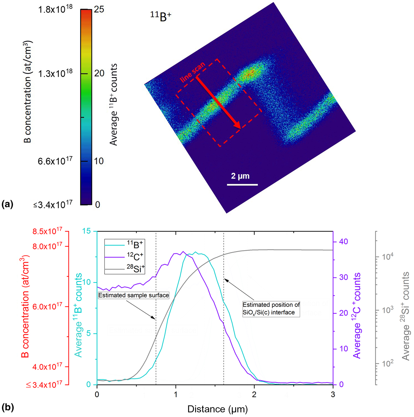
Figure 4. (a) SIMS image of 11B+ across a cross-section of pyramid multilayer structures and (b) intensity profiles of 11B+, 12C+, and 28Si+ across the multilayer stack as indicated by an arrow in (a). The integration width was 80 pixels (~3.1 µm). The boron intensities are converted to concentrations. Note that the quantification is applicable only in the Si substrate where the matrix is similar to the reference sample. The results indicate a gradual decrease in the B concentration in the substrate from ~6 × 10¹⁷ at./cm3 to levels below the detection limit.
In the experimental conditions used in this work, the SIMS image resolution is limited by the brightness of the duoplasmatron ion source. Although the resolution is relatively poor in this case, the primary oxygen ions are highly reactive, which enables high-sensitivity analysis required for the imaging of dopants. With modern high-brightness ion sources based on gas-field ion source (GFIS) technology such as in a helium ion microscope, ion probes of sufficient current can be focused to a sub-nm range.[Reference Notte, Huang, Hlawacek and Gölzhäuser18] In such cases, SIMS images are no longer limited by source brightness, but by the fundamental limit set by the size of the ion–solid interaction volume[Reference Wirtz, Philipp, Audinot, Dowsett and Eswara5] (~10 nm). Unfortunately, the GFIS technology is available only with noble gas ions (He+ and Ne+), which are not very reactive in comparison to oxygen or cesium. To overcome the SIMS image resolution limit, the SIMS images can be correlated with another high-resolution imaging technique such as TEM to reveal valuable insights related to the local nanoscale structure.[Reference Wirtz, Philipp, Audinot, Dowsett and Eswara5, Reference Yedra, Eswara, Dowsett and Wirtz6, Reference Vollnhals, Audinot, Wirtz, Mercier-Bonin, Fourquaux, Schroeppel, Kraushaar, Lev-Ram, Ellisman and Eswara19, Reference Eswara, Pshenova, Yedra, Hoang, Lovric, Philipp and Wirtz20]
Conclusions
A method to rapidly and quantitatively image dopant distribution using SIMS is demonstrated. The method is based on the cross-section analysis of a reference sample with a known concentration profile. For the investigated concentration range, a nonlinear relationship between 11B+ intensity and the concentration was observed. A SIMS detection limit of 3 (±2) × 1017 at./cm3 in the imaging mode with 39 nm pixel size was determined for the used experimental conditions. The method was demonstrated using an example of application with the analysis of dopant concentration in c-Si adjacent to a passivating contact stack of an annealed textured solar cell material. Because of the pixel nature of the SIMS images, a locally higher concentration at sub-pixel length scale cannot be captured, which is an inherent limitation of the SIMS imaging technique. Hence, the concentrations determined provide average values pixel by pixel.
Supplementary material
The supplementary material for this article can be found at https://doi.org/10.1557/mrc.2019.89.
Acknowledgments
This work was funded by the Luxembourg National Research Fund (FNR) through grant INTER/SNF/16/11536628 and by the Swiss National Science Foundation (SNF) within the bilateral project NACHOS. Prof. Roger Webb (Ion Beam Centre, Surrey, UK) is thanked for discussions related to ion implantation parameters used for the reference sample. Brahime El Adib (LIST) is thanked for his technical assistance with SIMS depth profiling.


 Open access