


Introduction
Scanning transmission electron microscopy (STEM) is a powerful method for investigating nanostructures. Standard STEM modes include bright-field (BF) for coherent phase-contrast imaging; annular bright-field (ABF) for partially coherent phase-contrast imaging; and incoherent bright-field (IBF), incoherent annular dark-field (ADF), and high-angle annular dark-field (HAADF) for Z-contrast imaging. Each of these imaging modes collects only part of the scattered electrons. As a result, in order to obtain a standard STEM image with signal-to-noise ratio comparable to that of a high-resolution transmission electron microscope (HRTEM) image, higher electron dose is required in the case of STEM imaging.
Phase-contrast techniques in STEM use efficiently the electrons within the BF cone for imaging, which not only improve the signal-to-noise ratio, but also provide more options to study nano- and low-Z materials. These techniques were first proposed in the 1970s (Dekkers & De Lang, Reference Dekkers and De Lang1974; Rose, Reference Rose1974, Reference Rose1977; Waddell & Chapman, Reference Waddell and Chapman1979) and extended in recent years by proposing different detector geometries and algorithms for handling the signals collected by the detector elements (Lohr et al., Reference Lohr, Schregle, Jetter, Wächter, Wunderer, Scholz and Zweck2012; Shibata et al., Reference Shibata, Findlay, Kohno, Sawada, Kondo and Ikuhara2012; Müller et al., Reference Müller, Krause, Béché, Schowalter, Galioit, Löffler, Verbeeck, Zweck, Schattschneider and Rosenauer2014; Majert & Kohl, Reference Majert and Kohl2015; Lazić et al., Reference Lazić, Bosch and Lazar2016; Lopatin et al., Reference Lopatin, Ivanov, Kosel and Chuvilin2016; Ophus et al., Reference Ophus, Ciston, Pierce, Harvey, Chess, McMorran, Czarnik, Rose and Ercius2016; Lee et al., Reference Lee, Kaiser and Rose2019). The most efficient STEM phase-contrast techniques are classified in two categories: (1) differential phase-contrast (DPC)-based techniques including (a) DPC, (b) integrated DPC (IDPC), and (c) differentiated DPC (DDPC); (2) center-of-mass (COM)-based techniques including (d) COM, (e) integrated COM (ICOM), and (f) differentiated COM (DCOM).
The standard DPC image can be acquired in two ways: (a) by using a Fresnel phase plate and (b) by subtracting the signals collected by two opposite segments of a sector detector, for example a quadrant detector. In the first method, the Fresnel phase plate is located at the front-focal plane of the objective lens. This phase plate can be realized either by adjusting the defocus and the correctable spherical aberrations appropriately (Rose, Reference Rose1974, Reference Rose1977) or by introducing a material phase plate (Ophus et al., Reference Ophus, Ciston, Pierce, Harvey, Chess, McMorran, Czarnik, Rose and Ercius2016). The introduction of the Fresnel phase plate results in constructive and destructive interference patterns on the detector. The interference pattern strongly depends on the geometry of the Fresnel phase plate. The intensities of the constructive and destructive interference regions are collected separately by the annular segments of the detector. The subtraction of these signals removes the nonlinear information and enhances the phase contrast (Rose, Reference Rose1977). Due to the application of an annular detector, this method is also named as annular differential phase contrast (ADPC) (Lee et al., Reference Lee, Kaiser and Rose2019). The proof of principle of this mode has been realized in a third-order spherical aberration-corrected scanning transmission electron microscope (STEM) operated at 300 kV, by inserting a physical Fresnel phase plate in front of the objective lens and by using a detector geometry which matches that of the Fresnel phase plate (Ophus et al., Reference Ophus, Ciston, Pierce, Harvey, Chess, McMorran, Czarnik, Rose and Ercius2016). According to our simulation studies, the depth of field in this mode could reach less than 3 Å for a C c/C 5-corrected STEM operating at 30 kV with an illumination aperture angle of 155 mrad. This condition allows optical sectioning of a thick sample (Lee et al., Reference Lee, Kaiser and Rose2019), at least in principle. Moreover, the practice requires that all non-spherically symmetric aberrations are sufficiently removed.
In the second DPC method, the difference signal is proportional to the tilt of the scattered electron beam, which is proportional to the strength of the lateral magnetic or electric field. By integrating or differentiating the DPC image along the symmetric axis of the opposite detector segments, one obtains the IDPC image or the DDPC image, respectively.
The DPC method shows its advantage in investigating dislocations (Denneulin et al., Reference Denneulin, Houdellier and Hÿtch2016), magnetic structures (Chapman & Scheinfein, Reference Chapman and Scheinfein1999), and electronic structures (Lohr et al., Reference Lohr, Schregle, Jetter, Wächter, Wunderer, Scholz and Zweck2012; Shibata et al., Reference Shibata, Findlay, Kohno, Sawada, Kondo and Ikuhara2012; Bauer et al., Reference Bauer, Hubmann, Lohr, Reiger, Bougeard and Zweck2014; Müller et al., Reference Müller, Krause, Béché, Schowalter, Galioit, Löffler, Verbeeck, Zweck, Schattschneider and Rosenauer2014). The DDPC method is preferred for measuring the charge-density distribution (Müller-Caspary et al., Reference Müller-Caspary, Krause, Grieb, Löffler, Schowalter, Béché, Galioit, Marquardt, Zweck, Schattschneider and Rosenauer2017). The IDPC method generates a map of the projected potential of the sample (Rose, Reference Rose1977; Lazić et al., Reference Lazić, Bosch and Lazar2016). The DPC obtained by an angular sector detector as well as the subsequent IDPC and DDPC constructs are usually applied for investigating thin samples, for which the effect of dynamical scattering is negligible.
The COM method multiplies the signal collected by each detector pixel with a displacement of the signal in momentum space. In other words, this method multiplies each Ronchigram with a split-detector function weighed by momentum. It is similar to the second DPC method, however, can only be realized by algorithm. Applying the COM method on a thin sample produces a gradient map of the sample potential. By integrating or differentiating the COM image of a thin sample, one obtains the potential map and charge density, respectively (Waddell & Chapman, Reference Waddell and Chapman1979; Lazić et al., Reference Lazić, Bosch and Lazar2016). As an alternative of the ICOM method in approximating the linear transfer of the sample potential, the IDPC method using a quadrant detector or an annular quadrant detector is an ideal tool for directly imaging the potential of a thin sample (Lazić et al., Reference Lazić, Bosch and Lazar2016). In this work, we propose a IDPC method using a multi-sector detector for imaging thick samples. The DPC- and COM-based methods are summarized in Figure 1.

Fig. 1. The phase-contrast technique in STEM has two categories: DPC-based and COM-based. The DPC method uses an annular detector or a sector detector. The IDPC and DDPC methods are extensions of the DPC method using angular sector detectors. The COM, ICOM, and DCOM methods use split-detector functions weighed by momentum, which is realized by algorithm.
Theory and Method
Theory
The introduction of our IDPC method using a multi-sector detector starts with a short overview of STEM imaging, the calculation of the corresponding contrast transfer function (CTF), and the formation of IDPC. Since we study the performance of the IDPC method for both C c/C 3-corrected and C 3-corrected STEM in this work, chromatic aberration is included in the overview.
Formation of STEM Images Including Chromatic Aberration
The interaction of the electron probe with an atom located at position  $\vec {\rho }_0$ is given by the product of the probe function $\Psi ( \vec {\rho }-\vec {\rho }_0,\; \Delta E)$ and the object transmission function $O( \vec {\rho })$: $\Psi ( \vec {\rho }-\vec {\rho }_0,\; \Delta E) O( \vec {\rho })$, where ΔE is the deviation of the electron energy from the mean energy E 0. The wave function $\Psi ( \vec {\rho },\; \Delta E)$ at the object plane z 0 is given by the following equation:
 $$\Psi( \vec{\rho},\; \Delta E) = FT[ \Psi_0A(\vec{\theta}) T_L( \vec{\theta},\; \Delta E) ] .$$
Here, Ψ0 is the incident plane wave. The aperture function A(θ) guarantees that the non-scattered beam is only transmitted if θ is smaller than the limiting aperture angle θ 0; the lens transfer function  $T_L( \vec {\theta },\; \Delta E) = {\rm e}^{-{\rm i}\gamma ( \vec {\theta },\; \Delta E) } = {\rm e}^{-{\rm i}[ \gamma _g( \vec {\theta }) + \gamma _c( \vec {\theta }, \Delta E) ] }$ depends on the phase shift ϒg(θ) resulting from the geometrical aberrations and the defocus of the objective lens, as well as the chromatic phase shift ϒc(θ,ΔE) = Cc(πΔE/λE0)θ2, where Cc is the chromatic aberration coefficient. The Ronchigram pattern recorded by the detector is given as follows:
 $$\eqalign{I( \vec{\Theta},\; \vec{\rho}_0,\; \Delta E) & = \left\vert \iint A( \vec{\theta}) T_L( \vec{\theta},\; \Delta E) O( \vec{\rho}) \, {\rm e}^{-{\rm i}k\vec{\rho}( \vec{\Theta}-\vec{\theta}) }\, {\rm e}^{-{\rm i}k\vec{\rho}_0\vec{\theta}}d^2\vec{\rho}d^2\vec{\theta}\right\vert ^2\cr & = \left\vert \int A( \vec{\theta}) T_L( \vec{\theta},\; \Delta E) \tilde{O}( \vec{\Theta}-\vec{\theta}) \, {\rm e}^{-{\rm i}k\vec{\rho}_0\vec{\theta}}d^2\vec{\theta} \right\vert ^2\cr & = \vert T( \vec{\Theta},\; \Delta E,\; \vec{\rho}_0) \otimes \tilde{O}( \vec{\Theta}) \vert ^2.}$$
Here  $\vec {\Theta }$ is the detector angle. The object spectrum $\tilde {O}( \vec {\Theta })$ is the Fourier transform of the object transmission function $O( \vec {\rho })$. The transfer function $T( \vec {\Theta },\; \Delta E,\; \vec {\rho }_0)$ is given as follows:
 $$T( \vec{\Theta},\; \Delta E,\; \vec{\rho}_0) = A( \vec{\Theta} ) T_L( \vec{\Theta},\; \Delta E) \, {\rm e}^{-{\rm i}k\vec{\rho}_0\vec{\Theta}}.$$
This function consists of the aperture function  $A( \Theta )$, the lens transfer function $T_L( \vec {\Theta },\; \Delta E)$, and the function ${\rm e}^{-{\rm i}k\vec {\rho }_0\vec {\Theta }}$ associating with the position of the probe.
A STEM image formed by a scanning probe of the energy E 0 + ΔE is given by the following equation:
 $$I( \vec{\rho}_0,\; \Delta E) = \int D( \vec{\Theta}) \vert T( \vec{\Theta},\; \Delta E,\; \vec{\rho}_0) \otimes \tilde{O}( \vec{\Theta}) \vert ^2 d^2\vec{\Theta}.$$
The detector function  $D( \vec {\Theta })$ accounting for the combination of the signals recorded by the individual elements of the detector has positive or negative values indicating signal subtraction. The absolute value of the detector function has the property $\vert D( \vec {\Theta }) \vert \leq 1$. In the case of perfect collection efficiency, the absolute value adopts its maximum $\vert D( \vec {\Theta }) \vert = 1$.
Electron waves of different energies are incoherent. As a result, the final image is a sum of subimages formed by scanning probes of different energies. Each subimage  $I ( \vec {\rho }_0,\; \Delta E)$ is weighted by a factor accounting for the contribution of the energy deviation ΔE, and the weighting factor is obtained from a normalized energy-loss spectrum p(ΔE), which satisfies $\int p( \Delta E) d\Delta E = 1$. The intensity distribution of the image is given as follows:
 $$\eqalign{I( \vec{\rho}_0) & = \int p( \Delta E) I ( \vec{\rho}_0,\; \Delta E) d\Delta E\cr & = \iint p( \Delta E) D( \vec{\Theta}) \vert T( \vec{\Theta},\; \Delta E,\; \vec{\rho}_0) \otimes \tilde{O}( \vec{\Theta}) \vert ^2 d^2\vec{\Theta}d\Delta E}.$$
In the case of C c-correction (γc = C c = 0), we can readily perform the ΔE integration, giving
 $$I( \vec{\rho}_0) = \int D( \vec{\Theta}) \vert T( \vec{\Theta},\; \vec{\rho}_0) \otimes \tilde{O}( \vec{\Theta}) \vert ^2 d^2\vec{\Theta}.$$
CTF for STEM Phase-Contrast Imaging
In order to derive the CTF for STEM phase-contrast imaging, we first take the Fourier transform of the image intensity distribution (5):
 $$\tilde{I}( \vec{\omega}) = FT[ I( \vec{\rho}_0) ] = \iiint p( \Delta E) D( \vec{\Theta}) \vert T( \vec{\Theta},\; \Delta E,\; \vec{\rho}_0) \otimes \tilde{O}( \vec{\Theta}) \vert ^2 \, {\rm e}^{-{\rm i}k\vec{\rho}_0\vec{\omega}}d\vec{\rho}_0 d^2\vec{\Theta}d\Delta E.$$
Here  $\vec {\omega } = \vec {\Theta }-\vec {\theta }$ represents the scattering angle. In the second step, we assume a thin sample and employ the weak-phase object approximation $O( \vec {\rho }) = {\rm e}^{{\rm i}V( \vec {\rho }) }\approx 1 + {\rm i}V( \vec {\rho })$. The Fourier transform gives the object spectrum:
 $$\tilde{O}( \vec{\Theta}) = \int {\rm e}^{{\rm i}V( \vec{\rho}) }\, {\rm e}^{-{\rm i}k\vec{\rho}\vec{\Theta}}d\vec{\rho}\approx{1\over k}[ \delta( \vec{\Theta}) + {\rm i}\tilde{V}( \vec{\Theta}) ] .$$
By substituting equation (8) for  $\tilde {O}( \vec {\Theta })$ in equation (7) and neglecting nonlinear terms, we obtain
 $$\eqalign{I( \vec{\omega}) & = {1\over k^2}\int A( \vec{\Theta}) D( \vec{\Theta}) d^2\vec{\Theta} \cr & \quad + {{\rm i}\over k^2}\iint p( \Delta E) A( \vec{\Theta}) D( \vec{\Theta}) { \tilde{V}( \vec{\omega}) A( \vec{\omega}-\vec{\Theta}) \, {\rm e}^{-{\rm i}[ \gamma( \vec{\omega}-\vec{\Theta}, \Delta E) -\gamma( \vec{\Theta}, \Delta E) ] } \cr & \quad-\tilde{V}^\ast ( {-}\vec{\omega}) A( \vec{\omega} + \vec{\Theta}) \, {\rm e}^{{\rm i}[ \gamma( \vec{\omega} + \vec{\Theta}, \Delta E) -\gamma( \vec{\Theta}, \Delta E) ] }} d^2\vec{\Theta}d\Delta E.}$$
The first term in equation (9) contributes to the background intensity. The aperture function  $A( \vec {\Theta })$ determines the quantity of electrons interacting with the sample, and the detector function $D( \vec {\Theta })$ determines the quantity of electrons for imaging. If there is no overlap between the illumination angle defined by the aperture and the collection angle of the detector, then $A( \vec {\Theta }) D( \vec {\Theta }) = 0$. In this case, equation (9) equals 0 and there is no phase contrast. We define $\Omega = \int A( \vec {\Theta }) D( \vec {\Theta }) d^2\vec {\Theta }$. In order to maximize the efficiency of the electron dose, all electrons should be collected for imaging, which means the collection angle equals at least the illumination angle θ 0. In this case, $\Omega = \int A( \vec {\Theta }) d^2\vec {\Theta } = \pi \theta _0^2$. Because $V( \vec {\rho })$ is a real function, Friedel's law shows $\tilde {V}( \vec {\omega }) = \tilde {V}^\ast ( {-}\vec {\omega })$. Using this relation and neglecting the first term, we rewrite equation (9) in the form $I( \vec {\omega }) = ( {\Omega }/{k^2}) B( \vec {\omega }) V( \vec {\omega })$.
 $$\eqalign{B( \vec{\omega}) & = {{\rm i}\over \Omega}\iint p( \Delta E) A( \vec{\Theta}) D( \vec{\Theta}) { A( \vec{\omega}-\vec{\Theta}) \, {\rm e}^{-{\rm i}[ \gamma( \vec{\omega}-\vec{\Theta}, \Delta E) -\gamma( \vec{\Theta}, \Delta E) ] }\cr & \quad-A( \vec{\omega} + \vec{\Theta}) \, {\rm e}^{{\rm i}[ \gamma( \vec{\omega} + \vec{\Theta}, \Delta E) -\gamma( \vec{\Theta}, \Delta E) ] }} d^2\vec{\Theta}d\Delta E.}$$
 Assuming that p(ΔE) is a normalized Gaussian function  $p( \Delta E) = ( {1}/{\sqrt {2\pi }\sigma _E}) \exp ( {-}{\Delta E^2}/{2\sigma _E^2})$, we can perform analytically the integral (10) with respect to ΔE, giving
 $$\eqalign{& E( \vec{\Theta},\; \vec{\omega}\pm\vec{\Theta}) \cr & = {1\over \sqrt{2\pi}\sigma_E}\int \exp\left(-{\Delta E^2\over 2\sigma_E^2}\right)\exp\left\{\mp {\rm i}C_c{\pi\Delta E\over \lambda E_0}[ ( \vec{\omega}\mp\vec{\Theta}) ^2-\vec{\Theta}^2] \right\}d\Delta E \cr & = \exp\left\{-{1\over 2}\left({\pi C_c \sigma_E\over \lambda E_0}\right)^2[ ( \vec{\omega}\mp\vec{\Theta}) ^2-\vec{\Theta}^2] ^2\right\}.}$$
Employing the focal spread  $\sigma _c = C_c ( {\sigma _E}/{E_0}) = C_c ( {\sqrt {\langle ( \Delta E) ^2\rangle }}/{E_0})$, we rewrite equation (11) in the form
 $$E( \vec{\Theta},\; \vec{\omega}\pm\vec{\Theta}) = \exp\left\{-{1\over 2}\left({\pi\sigma_c\over \lambda}\right)^2 [ ( \vec{\omega}\mp\vec{\Theta}) ^2-\vec{\Theta}^2] ^2\right\}.$$
In the case of chromatic correction,  $E( \vec {\omega }\mp \vec {\Theta },\; \vec {\Theta }) = 1$. By employing equations (12) and (11), the phase CTF (equation 10) adopts the form
 $$\eqalign{B( \vec{\omega}) & = {{\rm i}\over \Omega}\int A( \vec{\Theta}) D( \vec{\Theta}) { A( \vec{\omega}-\vec{\Theta}) E( \vec{\omega}-\vec{\Theta},\; \vec{\Theta}) \, {\rm e}^{-{\rm i}[ \gamma_g( \vec{\omega}-\vec{\Theta}) -\gamma_g( \vec{\Theta}) ] } \cr & \quad -A( \vec{\omega} + \vec{\Theta}) E( \vec{\omega} + \vec{\Theta},\; \vec{\Theta}) \, {\rm e}^{{\rm i}[ \gamma_g( \vec{\omega} + \vec{\Theta}) -\gamma_g( \vec{\Theta}) ] }} d^2\vec{\Theta} \cr & = {{\rm i}\over \Omega}\int L( \vec{\omega},\; \vec{\Theta}) d^2\vec{\Theta}.}$$
CTF for IDPC Imaging
The principle of the IDPC can be understood from a twin-pixel detector which consists of two pixels located at detector angles  $\vec {\Theta }$ and $-\vec {\Theta }$, respectively. The twin-pixel detector satisfies the relation: $D( \vec {\Theta }) = -D( -\vec {\Theta })$. The CTF $L( \vec {\omega },\; \vec {\Theta })$ of the DPC image formed by such a twin-pixel detector is derived from equation (13) and given by the following equation:
 $$\eqalign{L( \vec{\omega},\; \vec{\Theta}) & = A( \vec{\omega}-\vec{\Theta}) E( \vec{\omega}-\vec{\Theta},\; \vec{\Theta}) \cos[ \gamma_g( \vec{\omega}-\vec{\Theta}) -\gamma_g( \vec{\Theta}) ] \cr & \quad-A( \vec{\omega} + \vec{\Theta}) E( \vec{\omega} + \vec{\Theta},\; \vec{\Theta}) \cos[ \gamma_g( \vec{\omega} + \vec{\Theta}) -\gamma_g( \vec{\Theta}) ] .}$$
An IDPC image formed by a twin-pixel detector is obtained by integrating the DPC image along the direction parallel to the link of the twin pixels. Correspondingly, the CTF  $L( \vec {\omega },\; \vec {\Theta })$ for DPC imaging and the one $L_i( \vec {\omega },\; \vec {\Theta })$ for IDPC imaging are connected by the following relation:
 $$\int L( \vec{\omega},\; \vec{\Theta}) \, {\rm e}^{{\rm i}k\vec{\rho}\vec{\omega}}d^2\vec{\omega} = {d\over d\vec{\rho}_s}\int L_i( \vec{\omega},\; \vec{\Theta}) \, {\rm e}^{{\rm i}k\vec{\rho}\vec{\omega}}d^2\vec{\omega}.$$
Here,  $\vec {\rho }_s$ is a vector in real space parallel to the link of the twin pixels and thus can point in two possible directions. For a single atom, the DPC signal is antisymmetric (Shibata et al., Reference Shibata, Findlay, Kohno, Sawada, Kondo and Ikuhara2012). Therefore, the IDPC image obtained by integrating the DPC signal leads to either bright or dark atom contrast, depending on the direction of the integral. Using the following relations:
 $${d\over d\vec{\rho}_s} = \cos\Phi{d\over d\rho_x} + \sin\Phi{d\over d\rho_y},\; $$
 $$\vec{\rho}\vec{\omega} = \rho_x\omega_x + \rho_y\omega_y,\; $$
we obtain from equation (15)
 $$L( \vec{\omega},\; \vec{\Theta}) = {\rm i}k( \omega_x\cos\Phi + \omega_y\sin\Phi) L_i( \vec{\omega},\; \vec{\Theta}) ,\; $$
 $$L_i( \vec{\omega},\; \vec{\Theta}) = {\Theta_s\over {\rm i}k\Theta_s( \omega_x\cos\Phi + \omega_y\sin\Phi) }L( \vec{\omega},\; \vec{\Theta}) = {\Theta_s\over {\rm i}k\vec{\Theta}_s\vec{\omega}}L( \vec{\omega},\; \vec{\Theta}) .$$
 Here,  $\vec {\Theta }_s$ is a vector on the detector parallel to $\vec {\rho }_s$; Φ is the azimuthal angle of both vectors $\vec {\rho }_s$ and $\vec {\Theta }_s$. In the current IDPC mode, the DPC images are first acquired by subtracting the signals collected by opposite segments of a quadrant detector (Rose, Reference Rose1977; Lazić et al., Reference Lazić, Bosch and Lazar2016) or by an annular quadrant detector (Yücelen et al., Reference Yücelen, Lazić and Bosch2018). Then the IDPC image is obtained by integrating each of the two difference signals along the symmetric axis of the two opposite segments. This method has demonstrated experimentally its advantage by showing the images of heavy and light atoms simultaneously and by suppressing high-frequency noise (Rose, Reference Rose1977; Lazić et al., Reference Lazić, Bosch and Lazar2016). The CTF of the IDPC mode using a segment detector is obtained by replacing $L( \vec {\omega },\; \vec {\Theta })$ in equation (13) with $L_i( \vec {\omega },\; \vec {\Theta })$ in equation (19) and performing the integral over a detector segment. The CTF for the IDPC imaging by using a pair of quadrant detector sectors is given by the following equation:
 $$B_{{\rm idpc}}( \vec{\omega}) = {1\over k\Omega}\int_{\Phi_0}^{\Phi_0 + {\pi}/{2}}\int_0^{\theta_0}{\Theta_s\over \vec{\Theta}_s\vec{\omega}}L( \vec{\omega},\; \vec{\Theta}) \Theta d\Theta d\Phi.$$
Here, Φ0 is the starting angle for the quadrant sector. Instead of forming four quadrant sectors, we can divide the detector in n (n = 2m, m = 1, 2, 3, …) angular sectors. The subtending angle of each sector is 2π/n. In this case, the CTF of the IDPC mode resulting from two opposite detector elements located at the azimuth angle Φm = Φ0 + 2π(m − 1)/n is given as follows:
 $$B_{{\rm idpc}}^{( m) }( \vec{\omega}) = {1\over k\Omega}\int_{\Phi_m}^{\Phi_m + {2\pi}/{n}}\int_0^{\theta_0} {\Theta_s^{( m) }\over \vec{\Theta}_s^{( m) }\vec{\omega}}L( \vec{\omega},\; \vec{\Theta}) \Theta d\Theta d\Phi.$$
By summing up the IDPC images obtained from all detector sectors, the corresponding CTF is given by the following equation:
 $$\eqalign{\openup 2pt& B_{{\rm idpc}}( \vec{\omega}) \cr & = \sum_m B_{{\rm idpc}}^{( m) }( \vec{\omega}) \cr & = {1\over k\Omega}\sum_{m = 1}^{n}\int_{\Phi_0 + {2\pi ( m-1) }/{n}}^{\Phi_0 + {2\pi m}/{n}}\int_0^{\theta_0}{\Theta_s^{( m) }\over \vec{\Theta}_s^{( m) } \vec{\omega}} \cr & \quad { A( \vec{\omega}-\vec{\Theta}) E( \vec{\omega}-\vec{\Theta},\; \vec{\Theta}) \cos[ \gamma_g( \vec{\omega}-\vec{\Theta}) -\gamma_g( \vec{\Theta}) ] \cr & \quad -A( \vec{\omega} + \vec{\Theta}) E( \vec{\omega} + \vec{\Theta},\; \vec{\Theta}) \cos[ \gamma_g( \vec{\omega} + \vec{\Theta}) -\gamma_g( \vec{\Theta}) ] } \Theta d\Theta d\Phi.}$$
CTF for ICOM Imaging
By replacing  $D( \vec {\Theta })$ in equations (4) and (13) with $k\vec {\Theta }_x$ or $k\vec {\Theta }_y$, one obtains a COM image and the corresponding CTF, respectively. The functions $k\vec {\Theta }_x$ and $k\vec {\Theta }_y$ are antisymmetric about y-axis and x-axis, respectively. As a result, the CTFs for COM imaging can be analogically acquired by multiplying k|Θ x| or k|Θ y| with $L( \vec {\omega },\; \vec {\Theta })$ in equation (14) and integrating the product:
 $$B_{{\rm com}-x}( \vec{\omega}) = {{\rm i}k\over \Omega} \int_{\pi/2}^{3\pi/2}\int_0^{\theta_0} \vert \Theta_x\vert L( \vec{\omega},\; \vec{\Theta}) \Theta d\Theta d\Phi,\; $$
 $$B_{{\rm com}-y}( \vec{\omega}) = {{\rm i}k\over \Omega}\int_{0}^{\pi} \int_0^{\theta_0} \vert \Theta_y\vert L( \vec{\omega},\; \vec{\Theta}) \Theta d\Theta d\Phi.$$
The corresponding CTFs for ICOM imaging are given by the following equations:
 $$B_{{\rm icom}-x}( \vec{\omega}) = {1\over {\rm i}k\omega_x}B_{{\rm com}-x}( \vec{\omega}) = {1\over \omega_x\Omega}\int_{\pi/2}^{3\pi/2}\int_0^{\theta_0} \vert \Theta_x\vert L( \vec{\omega},\; \vec{\Theta}) \Theta d\Theta d\Phi,\; $$
 $$B_{{\rm icom}-y}( \vec{\omega}) = {1\over {\rm i}k\omega_y}B_{{\rm com}-y}( \vec{\omega}) = {1\over \omega_y\Omega}\int_{0}^{\pi}\int_0^{\theta_0} \vert \Theta_y\vert L( \vec{\omega},\; \vec{\Theta}) \Theta d\Theta d\Phi,\; $$
 $$B_{{\rm icom}}( \vec{\omega}) = B_{{\rm icom}-x}( \vec{\omega}) + B_{{\rm icom}-y}( \vec{\omega}) .$$
Method for Realizing the Functionality of a Multi-Sector Detector Using a Quadrant Detector
Proof-of-principle experiments were carried out by using a Thermofisher Talos 200× microscope operating at 200 kV (operated in STEM mode). The system is equipped with a standard 4-quadrant DPC detector from Thermofisher. In order to realize the functionality of a multi-sector detector using the current experiment setup, we propose the following strategy, exemplified for the case of a 12-sector detector.
By rotating the quadrant detector (A 1, B 1, C 1, D 1) in a step of 30° as illustrated in Figure 2, we obtain two configurations (A 2, B 2, C 2, D 2) and (A 3, B 3, C 3, D 3), respectively. The DPC signals formed by a pair of opposite segments of a 12-sector detector are calculated by the following relations:
 $$\matrix{&I_1-I_7 = A_1-A_2 + B_1-B_2\cr& I_2-I_8 = A_2-A_3 + B_2-B_3\cr & I_3-I_9 = A_3-B_1 + B_3-C_1\cr& I_4-I_{10} = B_1-B_2 + C_1-C_2\cr& I_5-I_{11} = B_2-B_3 + C_2-C_3\cr& I_6-I_{12} = B_3-C_1 + C_3-D_1 }$$
The IDPC images for each pair of opposite segments are obtained by integrating the DPC signal along the symmetric axis of the segments, and all IDPC images are summed up.

Fig. 2. The functionality of a 12-sector detector is realized by rotating a quadrant detector by 30 and 60°, respectively. The rotation of the quadrant detector (A 1, B 1, C 1, D 1) by 30 and 60° clockwise results in the configurations (A 2, B 2, C 2, D 2) and (A 3, B 3, C 3, D 3), respectively. The DPC signals formed by a pair of opposite segments of a 12-sector detector are calculated by the relations in equation (28).
In practice, we achieved the rotation of the detector by manual in-plane rotation in steps of 30° of the sample using a Fischione 2040 dual-axis tomography holder. For each rotation, four images were acquired from the four detector segments simultaneously together with an HAADF image as reference for alignment. The images corresponding to the detector sets (A 2, B 2, C 2, D 2) and (A 3, B 3, C 3, D 3) are rotated 30 and 60° with reference to the images acquired by the detector set (A 1, B 1, C 1, D 1), respectively. As a result, the rotated images need to be rotated back to align with the reference image before the postprocessing procedure using the relations in equation (28).
Result and Discussion
Influence of the Number of Detector Sectors on IDPC-STEM Imaging
Simulations
In order to investigate the influence of the number of detector segments on the CTF of the IDPC mode, we approximate the phase shift  $\gamma _g( \vec {\Theta })$ in equation (22) by the following equation:
 $$\gamma_g( \Theta) = -{\pi\over \lambda}\left(\Delta f\Theta^2 + {1\over 2}C_3\Theta^4 + {1\over 3}C_5\Theta^6\right).$$
Here, λ is the wavelength of the electron. For a C c/C 3-corrected or a C 3-corrected microscope, the fifth-order spherical aberration coefficient C 5 is fixed. By properly adjusting the defocus Δf and the third-order spherical aberration coefficient C 3, one can optimize the phase shift γ(Θ) (Lentzen, Reference Lentzen2008).
Figure 3 shows the CTFs of the IDPC mode for each of four different detectors and several defoci calculated based on equation (22). The calculations are performed for a C c/C 3-corrected STEM and a C 3-corrected STEM with C c = 1.2 mm operating at the accelerating voltage U = 80 kV. The fifth-order spherical aberration coefficient is C 5 = 2 mm. The third-order spherical aberration coefficient C 3 and the defocus are optimized based on C 5. The maximum illumination angle is mainly determined by chromatic aberration. Without C c-correction, the illumination angle is around 30 mrad at 80 kV, and is supposed to reach 62 mrad in the case of C c-correction. Although such a high value is not yet realized in practice, we present the calculations in order to show the influence and potential of C c-correction for the IDPC imaging. The term df 0 represents a sharp focus at the top surface of the sample. For depth-sectioning of a thick sample, the probe is focussed at different planes within the thick sample by introducing an extra underfocus. The CTFs at different defocus values actually demonstrate the performance of the IDPC mode for imaging distinct slices within the sample.

Fig. 3. Calculated CTFs for (a) C c/C 3-corrected and (b) C 3-corrected IDPC-STEM by using 4, 8, 12, and 18 detector segments at different defoci. Defocus 0 represents the optimum defocus df 0. The defocus increases from left to right in a step of 1 nm. Microscope parameters: U = 80 kV, C 5 = 2 mm, C 3 = −7.77 μm, df 0 = 61 Å. For (a) C c/C 3-corrected microscope: θ0 = 62 mrad. For (b) C 3-corrected microscope: C c = 1.2 mm, σc = 4 nm, θ 0 = 30 mrad.
Figure 3 shows that, with only four detector sectors, the anisotropy of the CTF increases along with defocus for both C c/C 3-corrected and C 3-corrected STEM (1st row of Figs. 3a and 3b). This behavior can lead to a non-interpretability of the IDPC image at large defoci. By increasing the number of detector segments, the isotropy of the CTF improves remarkably, as shown by the CTF for detectors using 8, 12, and 18 sectors (2nd to 4th rows of Figs. 3a and 3b). In the case of C c/C 3-corrected STEM, the CTF is already largely rotationally symmetric at all given defocus values up to 10 nm by using 18 detector sectors. In the case of C 3-corrected STEM with C c = 1.2 mm, only 8 detector sectors are required for generating rotationally symmetric CTFs at all given defocus values. Figure 3 shows that the resolution limit improves for the IDPC mode as chromatic aberration is corrected. However, for the depth sectioning of a thick sample, fewer detector sectors are required in order to generate an isotropic CTF for a C c-uncorrected STEM compared with a C c-corrected STEM.
In order to verify the reduction of the CTF anisotropy for IDPC-STEM imaging by increasing the number of detector segments, we simulated C c/C 3-corrected and C 3-corrected IDPC-STEM focal series of a heterostructure consisting of a polyoxometalate (POM) particle stuffed in a single-wall carbon nanotube (Fig. 4 left). The multislice algorithm (Kirkland, Reference Kirkland1998) has been applied for the image calculation by assuming the Wentzel potential (Wentzel, Reference Wentzel1926) for atoms. The accelerating voltage is 80 kV and the illumination is parallel to the tubular axis of the nanotube. Detectors with 4, 8, 12, 18, 40, and 80 sectors are applied. It is quite challenging to realize a 40-segment detector physically, not to mention a 80-segment detector. However, a pixelated detector enables one to generate any detector geometry. In our calculations, all segment detectors are simulated by assuming a pixelated detector. As a comparison with the IDPC imaging, the focal-series calculations for the ICOM imaging are also presented. In the case of C c/C 3-correction, image contrast and resolution are higher than in the case of only C 3-correction. By using four detector sectors for the IDPC imaging, the anisotropy of the CTF introduces stripe-like artefacts in the images, as shown by the first column of Figures 4a and 4b. Increasing the number of detector sectors removes the artifacts gradually and enhances the contrast. As the probe focusses at the plane located at 4.5 nm from the top, a sharp image of the tungsten aluminum oxide particle shows up if more than 18 detector sectors are employed for the C c/C 3-corrected STEM and C 3-corrected STEM, although the resolution is much lower in the latter case. Despite multiple scattering within the sample, the improved IDPC method is still able to suppress the dynamical effect.

Fig. 4. Simulations of (a) C c/C 3-corrected and (b) C 3-corrected IDPC/ICOM-STEM focal series. The IDPC calculations use different numbers of detector segments. The sample is a heterostructure consisting of a polyoxometalate (POM) particle stuffed in a single-wall carbon nanotube (left). The images in each row are simulated for a given location of the probe focus. Microscope parameters: U = 80 kV, C 5 = 2 mm, C 3 = −7.77 μm, df 0 = 61 Å. For (a) C c/C 3-corrected microscope: θ0 = 62 mrad. For (b) C 3-corrected microscope: C c = 1.2 mm, σc = 4 nm, θ 0 = 30 mrad. Scale bar: 0.5 nm.
For the ICOM imaging, stripes are present similar to the case of the IDPC imaging using a quadrant detector, as shown in the last column of Figures 4a and 4b. However, the anisotropy effect can be reduced by expanding the field of view in the calculation for ICOM images (Lazić et al., Reference Lazić, Bosch and Lazar2016). The field of view is the reciprocal of the sampling in q-space. In our case, the field of view is about 1.5 nm, resulting in a sampling of 0.066 Å−1/pixel in q-space. The examples presented in Lazić et al. (Reference Lazić, Bosch and Lazar2016) have a field of view of 5 nm, corresponding to a sampling of 0.02 Å−1/pixel in q-space. Figure 5 shows the calculated CTFs for ICOM imaging at q-samplings of 0.066 and 0.02 Å−1/pixel, respectively. The calculations adopted the same focal values as in Figure 4 and were performed for C c/C 3-corrected and C 3-corrected STEM. For the q-sampling of 0.066 Å−1/pixel, anisotropy is present in the CTFs for both the C c/C 3-corrected and C 3-corrected ICOM imaging. However, a q-sampling of 0.02 Å−1/pixel results in isotropic CTFs for all cases.

Fig. 5. Calculated CTFs for (a) C c/C 3-corrected and (b) C 3-corrected ICOM imaging by applying different q-samplings and focal values. Microscope parameters: U = 80 kV, C 5 = 2 mm, C 3 = −7.77 μm, df 0 = 61Å. For (a) C c/C 3-corrected microscope: θ 0 = 62 mrad. For (b) C 3-corrected microscope: C c = 1.2 mm, σc = 4 nm, θ 0 = 30 mrad.
Figure 6 shows average of the 2D CTFs over the azimuthal angle in the case of C c/C 3-corrected and C 3-corrected IDPC/ICOM-STEM imaging. For the IDPC imaging, 4, 8, 12, 18, 40, and 80 detector sectors are applied, respectively. The CTF curves start with unity at the origin q = 0 (q = ω/λ). In the C c/C 3-corrected case, the CTFs for both the ICOM and IDPC imaging are more susceptible to focal variation than the C 3-corrected case. Although the contrast and resolution are significantly lower in the C 3-corrected case at the optimum defocus df 0, the performance of the IDPC and ICOM imaging in this case is quite stable up to large sample thicknesses. For the IDPC imaging, the transfer function B(q) improves at low frequency region as the number of detector sector increases. The introduction of underfocus in the C c/C 3-corrected case enhances image contrast at the expense of resolution, as shown by the CTF curves for df 0 − 4.5 nm and df 0 − 9 nm in Figure 6a. This behavior is also demonstrated by the calculated IDPC images using more than 12 detector sectors in Figure 4a. The contrast of the carbon wall increases as the probe moves downwards; meanwhile, its resolution deteriorates. The IDPC imaging mode has a potential for imaging extended structures of biological objects with high contrast without the need of large defoci, as it is the case for the TEM. Image contrast of large object details improves with increasing defoci and increasing detector sectors.

Fig. 6. Profiles of CTFs for (a) C c/C 3-corrected and (b) C 3-corrected IDPC/ICOM-STEM imaging at different defoci. The IDPC calculations use 4, 8, 12, 18, 40, and 80 detector sectors. Microscope parameters: U = 80 kV, C 5 = 2 mm, C 3 = −7.77 μm, df 0 = 61 Å. For (a) C c/C 3-corrected microscope: θ 0 = 62 mrad. For (b) C 3-corrected microscope: C c = 1.2 mm, σc = 4 nm, θ 0 = 30 mrad.
The interpretability of the IDPC images improves notably by increasing the number of detector sectors. This improvement is indispensable for imaging thick samples, because optical sectioning of a thick sample requires an isotropic CTF for obtaining a sufficient depth resolution. The depth resolution d d is inversely proportional to the square of the illumination aperture angle θ 0:
 $$d_d\approx 2{\lambda\over \theta_0^2}.$$
At 80 kV, the illumination aperture angles are θ 0 = 62 mrad for the C c/C 3-corrected STEM and θ 0 = 30 mrad for the C 3-corrected STEM in the examples above. By applying equation (30), we obtain the depth resolution d d ≈ 2.2 nm for the C c/C 3-corrected STEM and d d ≈ 9.2 nm for the C 3-corrected STEM in these cases.
Proof-of-Principle Experiment
We demonstrate the potential of the IDPC technique using a multi-sector detector by imaging multilayers of InGaN/GaN-quantum well structures on a 1 μm GaN layer on sapphire (0001) substrate. The sample was prepared in cross-section by gluing a sandwich, followed by mechanical grinding, polishing, dimpling, and subsequent Ar ion milling. The thickness of the cross-section sample is about 30 nm and the sample was cut along  $[ 11\bar {2}0]$ direction. The experiment has been carried out by using a Thermofisher Talos 200× microscope operating at 200 kV (operated in STEM mode, θ 0 = 10.5 mrad). A HAADF image and EDX maps of the sample are shown in Figure 7. The functionality of a 12-sector detector has been realized by the method described in the section “Method for Realizing the Functionality of a Multi-Sector Detector using a Quadrant Detector”. After each in-plane rotation of the sample holder, the sample position was readjusted and the focus was set to about −20 nm in order to focus the beam at the same plane within the sample. Since our method for realizing the 12-sector detector involves manual rotation of the sample and the post-processing includes image rotation, alignment, and cropping, a large field of view is necessary. Moreover, a 2k × 2k camera has been applied for exposures, and thus atomic resolution could not be achieved. However, the results are sufficient to demonstrate the potential of the IDPC method. Experiments using a pixelated detector should render better images than our proof-of-principle results.

Fig. 7. HAADF image and EDX maps of the InGaN/GaN layers. The images were recorded by using a Thermofisher Talos 200× microscope operating at 200 kV.
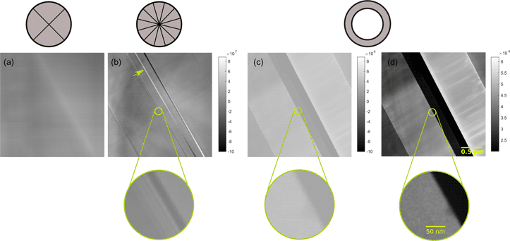
Figure 8 shows different experimental STEM images of the sample region. The images are obtained by using (Fig. 8a) the IDPC mode with fixed quadrant detector, (Fig. 8b) the IDPC mode applying the analogue of a 12-sector detector, and (Figs. 8c, 8d) the HAADF mode. The two IDPC images (Figs. 8a–b) are shown by using the same grayscale map: the lowest intensity of the two images is displayed as black, and the highest intensity is displayed as white. However, the same grayscale map cannot be applied for the HAADF image because the intensities of the HAADF image and the IDPC images are not of the same magnitude. The HAADF image in Figure 8c is displayed by using the grayscale map of the IDPC images scaled by a factor of 10−3. Unlike the IDPC images, the intensity of the HAADF image is always positive. This scaled grayscale map including negative values results in low display contrast of the HAADF image. By applying a grayscale map adapted to the intensity range of the HAADF image, one obtains Figure 8d.

Fig. 8. Experimental images of InGaN/GaN quantum wells on a 1 μm thick GaN prepared in cross-section. Images were obtained at an accelerating voltage of 200kV and the probe focuses at a plane 20nm away from the sample surface. Methods for acquiring the images include: (a) the IDPC mode employing the fixed quadrant detector, (b) the IDPC mode applying the described virtual 12-sector detector, and (c,d) the HAADF mode. The HAADF image (c) is displayed by using the grayscale map of the IDPC images scaled by a factor of 10−3, and the HAADF image (d) is the same image shown by applying a grayscale map adapted to its own intensity range. The illumination angle is 10.5 mrad. The collection angle is 8–20 mrad for the DPC mode, and 21–125 mrad for the HAADF mode. The images were recorded with a sampling of 2 nm/pixel.
As the probe focusses at a sample slice 20 nm away from the top, the IDPC image Figure 8a formed by the quadrant detector is not interpretable due to the anisotropy of the CTF. In contrast, the IDPC image Figure 8b formed by a virtual 12-sector detector shows much better resolution and contrast. It shows phase details, which are not visible in the HAADF image (Figs. 8c, 8d). One example is the white interface along the glue line marked by the arrow in panel b. Another example is the same region framed by the circles in Figures 8b–8d. The magnified image below Figure 8b shows the InGaN/GaN layers, which are not resolved in the HAADF image (Figs. 8c, 8d). The large underfocus 20 nm is not optimal for the HAADF imaging. Besides, the image recorded at low magnification suffers contrast lost due to the influence of the modulation-transfer function (MTF) of the camera (Thust, Reference Thust2009).
How Many Detector Sectors Are Necessary for the IDPC Imaging?
Figure 3 shows that the anisotropy of the CTF for the IDPC imaging mode using a quadrant detector enhances with increasing defocus or sample thickness at 80 kV. Up to a sample thickness of 10 nm, at least 18 detector sectors are required to produce an isotropic CTF for any plane within the object in the case of a C c/C 3-corrected STEM and at least 8 detector sectors are required in the case of a C 3-corrected STEM with chromatic aberration.
In this section, we explore the minimum number of detector sectors for the IDPC imaging at given sample depth and the study is exemplified for 80 kV. Instead of calculating the CTF for all the detector segments, we only calculate the CTF for one pair of detector segments based on equation (21). The CTF for any other pair of detector segments can be obtained through rotating the calculated CTF by an integer times of the angle  $360m/n\; \ ( m = 1,\; 2,\; 3\ldots,\ n-1)$. Here, n is the total number of detector segments. In order to simplify the calculation, we can assume that the pair of detector segments is located along the x-axis, as shown in Figure 9a, exemplified by the segments of a 12-sector detector. We have calculated the corresponding CTF for the IDPC imaging using this pair of detector segments by assuming that the probe focuses at a plane within the sample (Fig. 9b). The CTF (Fig. 9b) is then transformed to cartesian coordinates (Fig. 9c). By summing up all the rows of the transformed CTF (Fig. 9c), we obtain the line profile in Figure 9d. The full-width half maximum (FWHM) of each peak is denoted by w. In order to suppress anisotropy of the CTF for IDPC imaging, the minimal number of detector segments should be at least 360/w. Otherwise, the number of detector sectors is insufficient for the IDPC imaging at the given defocus or sample thickness.

Fig. 9. Procedure for determining whether a given number of detector segments is sufficient for the IDPC imaging at known sample depth, exemplified by Cc/C 3-corrected IDPC imaging at 80kV using a 12-sector detector with the probe focusing at a plane 6nm away from the sample surface. (a) A pair of detector segments extracted from a 12-sector detector; (b) calculated CTF for IDPC imaging by using the pair of detector segments in (a); (c) the CTF transformed in cartesian coordinates; (d) line profile obtained by summing up all rows of the transformed CTF. The FWHM of each peak is denoted by w. In order to avoid anisotropy of the CTF for the IDPC imaging, the number of detector segments should be more than 360/w.
We evaluated the performance of multi-sector detectors for the IDPC imaging at 80 kV and at different sample depths. We summarized the minimal numbers of detector sectors required for the IDPC imaging with isotropic CTF in Figure 10. For a C 3-corrected STEM, 8 detector sectors are sufficient for imaging up to a sample thickness of 25 nm. For a C c/C 3-corrected STEM, the minimal number of detector segments required for IDPC imaging increases almost linearly to the sample thickness of below 10 nm and above a sample thickness of 10 nm, at least 18 detector segments are required for the IDPC imaging.

Fig. 10. Minimum number of detector segments required for IDPC imaging of different cross-sections of thick samples using a C c/C 3-corrected STEM or a C 3-corrected STEM with C c = 1.2 mm at 80 kV.
Conclusion
We reported on IDPC-STEM for imaging thick samples, both exploring the potential by calculations and applying the method in a proof-of-principle experiment. We found from focal-series calculations applying a standard quadrant detector that the anisotropy of the CTF enhances strongly at the higher defoci resulting in uninterpretable image contrast, which is not the case, when using a multi-sector detector for IDPC imaging. Sector number-dependent calculations for both C c/C 3-corrected and C 3-corrected STEM have shown that increasing the number of detector sectors not only results in almost isotropic contrast transfer, but also enhances the image contrast and resolution. We suggest that the enhanced contrast at low spatial frequencies will be extremely helpful for imaging biological samples effectively without applying a large defocus or using a phase plate. Our calculations for ICOM imaging showed that a small field of view can lead to anisotropy of the CTF with this method. In our proof-of-principle IDPC experiment performed at an uncorrected STEM, we developed a procedure to realize the functionality of a 12-sector detector from a physical quadrant detector. As example, we used an InGaN/GaN quantum well structure and demonstrated the improvement in image contrast and resolution compared to the case using a standard quadrant detector. We further explored the minimal number of detector segments required to obtain an isotropic CTF for IDPC imaging at different sample thicknesses by calculations exemplified for C c/C 3-corrected and C 3-corrected STEM operating at 80 kV.
Acknowledgments
We gratefully acknowledge the financial support of the German Research Foundation (DFG) within the project 456681676.
Conflict of interest
The authors declare that they have no competing interest.


 Open access