


 where α = kT/EV, NV
is the effective density of states of the valence band, and gV
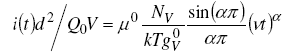
0 is the density-of-states (cm-3eV-1) for the valence bandtail at the upper edge of the valence band. The second source is the relationship NV/gV0 = kT (1-α) that obtains from the assumption that the valence band edge lies within the exponential bandtail (E. A. Schiff, Solar Energy Materials and Solar Cells, in press (2003).
where α = kT/EV, NV
is the effective density of states of the valence band, and gV
0 is the density-of-states (cm-3eV-1) for the valence bandtail at the upper edge of the valence band. The second source is the relationship NV/gV0 = kT (1-α) that obtains from the assumption that the valence band edge lies within the exponential bandtail (E. A. Schiff, Solar Energy Materials and Solar Cells, in press (2003).Crossref Citations
This article has been cited by the following publications. This list is generated based on data provided by Crossref.
Brinza, Monica
Emelianova, Evguenia V.
and
Adriaenssens, Guy J.
2006.
Link between enhanced carrier mobilities and DOS profiles in a-Si:H.
Thin Solid Films,
Vol. 511-512,
Issue. ,
p.
593.
Schiff, E.A.
2006.
Hole mobilities and the physics of amorphous silicon solar cells.
Journal of Non-Crystalline Solids,
Vol. 352,
Issue. 9-20,
p.
1087.
Lopes, V. C.
Hanson, E.
Whitfield, D.
Shrestha, K.
Littler, C. L.
and
Syllaios, A. J.
2013.
Temperature Dependence of 1/f Noise and Electrical Conductivity Measurements on p-type a-Si:H Devices.
MRS Proceedings,
Vol. 1536,
Issue. ,
p.
181.
Müller, Thomas Christian Mathias
Pieters, Bart Elger
Kirchartz, Thomas
Carius, Reinhard
and
Rau, Uwe
2014.
Effect of localized states on the reciprocity between quantum efficiency and electroluminescence in Cu(In,Ga)Se2 and Si thin-film solar cells.
Solar Energy Materials and Solar Cells,
Vol. 129,
Issue. ,
p.
95.
Lopes, V.C.
Syllaios, A.J.
and
Littler, C.L.
2017.
Low frequency noise in hydrogenated p-type amorphous silicon thin films.
Journal of Non-Crystalline Solids,
Vol. 459,
Issue. ,
p.
176.
Reynolds, Stephen
Brinza, Monica
Benkhedir, Mohammed L.
and
Adriaenssens, Guy J.
2017.
Springer Handbook of Electronic and Photonic Materials.
p.
1.
de Vrijer, Thierry
Bouazzata, Bilal
Ravichandran, Ashwath
van Dingen, Julian E. C.
Roelandschap, Paul J.
Roodenburg, Koos
Roerink, Steven J.
Saitta, Federica
Blackstone, Thijs
and
Smets, Arno H. M.
2022.
Opto‐Electrical Properties of Group IV Alloys: The Inherent Challenges of Processing Hydrogenated Germanium.
Advanced Science,
Vol. 9,
Issue. 18,