


No CrossRef data available.
Article contents
Robust resistive switching performance of pulsed laser deposited SiC/Ag/SiC tri-layer thin films deposited on a glass substrate
Published online by Cambridge University Press: 15 May 2020
Abstract
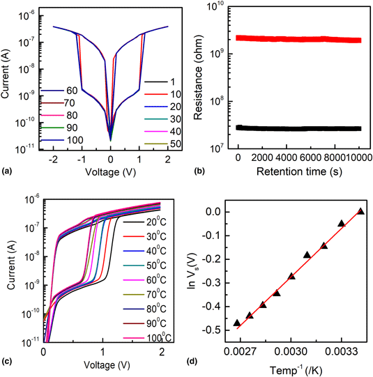
In this work, the authors developed SiC(10 nm)/Ag/SiC(10 nm) thin films showing an electroforming-free resistive switching (RS) effect with a switching ratio of 102. The observed RS effect is attributed to charging and discharging of Ag nanoparticles in the film layer. Further, SiC/Ag/SiC film shows an excellent endurance and retention as well as a good thermal stability of RS characteristics. It is also identified that the switching ratio is invariant but the switching voltage of the device greatly depends on the Ag nanoparticles concentration and the operation temperature of the device. Therefore, SiC/Ag/SiC thin films are attractive for next-generation memory devices with enhanced durability.
- Type
- Research Letters
- Information
- Copyright
- Copyright © Materials Research Society, 2020
References
Brewer, J.E. and Gill, M.: Nonvolatile Memory Technologies with Emphasis on Flash: A Comprehensive Guide to Understanding and Using Flash Memory Devices (John Wiley & Sons, New York, 2010).Google Scholar
Chiu, F.C., Shih, W.C., and Feng, J.J.: Conduction mechanism of resistive switching films in MgO memory devices. J. Appl. Phys. 111, 094104 (2012).CrossRefGoogle Scholar
Sawa, A.: Resistive switching in transition metal oxides. Mater. Today 11, 28 (2008).CrossRefGoogle Scholar
Waser, R., Dittmann, R., Staikov, G., and Szot, K.: Redox-based resistive switching memories – nanoionic mechanisms, prospects, and challenges. Adv. Mater. 21, 2632 (2009).CrossRefGoogle Scholar
Lin, C.C., Lin, C.Y., Lin, M.H., Lin, C.H., and Tseng, T.Y.: Voltage-polarity-independent and high-speed resistive switching properties of V-doped SrZrO3 thin films. IEEE Trans. Electron Devices 54, 3146 (2007).CrossRefGoogle Scholar
Ielmini, D., Nardi, F., and Cagli, C.: Universal reset characteristics of unipolar and bipolar metal-oxide RRAM. IEEE Trans. Electron Devices 58, 3246 (2011).CrossRefGoogle Scholar
Chen, C., Yang, Y.C., Zeng, F., and Pan, F.: Bipolar resistive switching in Cu/AlN/Pt nonvolatile memory device. Appl. Phys. Lett. 97, 083502 (2010).CrossRefGoogle Scholar
Ekström, M.: SiC CMOS and memory devices for high-temperature integrated circuits. Ph.D. Thesis, KTH Royal Institute of Technology, Stockholm, Sweden, 2019.Google Scholar
Lee, W., Park, J., Son, M., Lee, J., Jung, S., Kim, S., Park, S., Shin, J., and Hwang, H.: Excellent state stability of Cu/SiC/Pt programmable metallization cells for nonvolatile memory applications. IEEE Electron Device Lett. 32, 680 (2011).CrossRefGoogle Scholar
Zhong, L., Reed, P.A., Huang, R., De Groot, C.H., and Jiang, L.: Amorphous SiC based non-volatile resistive memories with ultrahigh ON/OFF ratios. Microelectron. Eng. 119, 61–64 (2014).CrossRefGoogle Scholar
Zhong, L., Jiang, L., Huang, R., and De Groot, C.H.: Nonpolar resistive switching in Cu/SiC/Au non-volatile resistive memory devices. Appl. Phys. Lett. 104, 093507 (2014).CrossRefGoogle Scholar
Morgan, K.A., Fan, J., Huang, R., Zhong, L., Gowers, R., Ou, J.Y., Jiang, L., and De Groot, C.H.: Active counter electrode in a SiC electrochemical metallization memory. J. Phys. D Appl. Phys. 50, 325102 (2017).CrossRefGoogle Scholar
Singh, N., Singh, K., and Kaur, D.: Bipolar resistive switching characteristics of silicon carbide nitride (SiCN)-based devices for nonvolatile memory applications. Ceram. Int. 43, 8970–8974 (2017).CrossRefGoogle Scholar
Fan, J., Jiang, L., Wang, S., Huang, R., Morgan, K.A., Zhong, L., and Groot, C.H.: Amorphous SiC resistive memory with embedded Cu nanoparticles. Microelectron. Eng. 174, 1–5 (2017).CrossRefGoogle Scholar
Kamakshi, K., Sekhar, K.C., Almeida, A., Agostinho Moreira, J., and Gomes, M.J.M.: Surface plasmon resonance-coupled photoluminescence and resistive switching behavior of pulsed laser-deposited Ag:SiC nanocermet thin films. Plasmonics 10, 1211 (2015).CrossRefGoogle Scholar
Manifacier, J.C., Gasiot, J., and Fillard, J.P.: A simple method for the determination of optical constants n, k and the thickness of a weakly absorbing thin film. J. Phy. E Sci. Instrum. 9, 1002 (1976).CrossRefGoogle Scholar
Zou, X., Ong, H.G., You, L., Chen, W., Ding, H., Funakubo, H., Chen, L., and Wang, J.: Charge trapping-detrapping induced resistive switching in Ba0.7Sr0.3TiO3. AIP Adv. 2, 032166 (2012).CrossRefGoogle Scholar
Fang, Y.C., Li, X.X., Blinn, K., Mahmoud, M.A., Liu, M.L., and Vac, J.: Resonant surface enhancement of Raman scattering of Ag nanoparticles on silicon substrates fabricated by dc sputtering. Sci. Technol. A 30, 050606 (2012).Google Scholar
Weimer, W.A. and Dyer, M.J.: Tunable surface plasmon resonance silver films. Appl. Phys. Lett. 79, 19 (2001).CrossRefGoogle Scholar
Wang, X., Li, M., Meng, L., Lin, K., Feng, J., Huang, T., Yang, Z., and Ren, B.: Probing the location of hot spots by surface-enhanced Raman spectroscopy: toward uniform substrates. ACS Nano 8, 528–536 (2014).CrossRefGoogle ScholarPubMed
Sun, H., Liu, Q., Long, S., Lv, H., Banerjee, W., and Liu, M.: Multilevel unipolar resistive switching with negative differential resistance effect in Ag/SiO2/Pt device. J. Appl. Phys. 116, 154509 (2014).CrossRefGoogle Scholar
Berciaud, S., Cognet, L., Tamarat, P., and Lounis, B.: Observation of intrinsic size effects in the optical response of individual gold nanoparticles. Nano. Lett. 5, 515 (2005).CrossRefGoogle ScholarPubMed
Yang, J.J., Miao, F., Pickett, M.D., Ohlberg, D.A., Stewart, D.R., Lau, C.N., and Williams, R.S.: The mechanism of electroforming of metal oxide memristive switches. Nanotechnology 20, 215201 (2009).CrossRefGoogle Scholar
Verrelli, E., Tsoukalas, D., Normand, P., Kean, A.H., and Boukos, N.: Forming-free resistive switching memories based on titanium-oxide nanoparticles fabricated at room temperature. Appl. Phys. Lett. 102, 022909 (2013).CrossRefGoogle Scholar
Silva, J.P.B., Kamakshi, K., Sekhar, K.C., Queirós, E.C., Agostinho Moreira, J., Almeida, A., Pereira, M., Tavares, P.B., and Gomes, M.J.M.: Resistive switching in ferroelectric lead-free 0.5Ba (Zr0.2Ti0.8)O3–0.5(Ba0.7Ca0.3)TiO3 thin films. J. Phys. D Appl. Phys. 49, 335301 (2016).CrossRefGoogle Scholar
Sekhar, K.C., Kamakshi, K., Bernstorff, S., and Gomes, M.J.M.: Effect of annealing temperature on photoluminescence and resistive switching characteristics of ZnO/Al2O3 multilayer nanostructures. J. Alloys Compd. 619, 248–252 (2015).CrossRefGoogle Scholar
Shin, J.W., Kim, S.H., and Cho, W.J.: Investigation on resistive switching characteristics of SiC and HfOx stacked nonvoltaile memory by microwave irradiation. Semicond. Sci. Technol. 34, 095006 (2019).CrossRefGoogle Scholar
Gogurla, N., Mondal, S.P., Sinha, A.K., Katiyar, A.K., Banerjee, W., Kundu, S.C., and Ray, S.K.: Transparent and flexible resisitve switching memory device with a very high On/OFF ratio using gold nanoparticles embedded in a silk protein matrix. Nanotechnology 24, 345202 (2013).CrossRefGoogle Scholar
Kao, K.C. and Huang, W.: Electrical Transport in Solids (Pergamon, Oxford, 1981) p. 150.Google Scholar