


Introduction
As the transistor feature sizes continue to scale ever smaller there has been a transition away from the use of conventional materials for the channel, Si, and the gate oxide, SiO2.[ Reference Goley and Hudait 1 ] Germanium has electron and hole mobility of 3900 and 1900 cm2/Vs, respectively, compared with 1400 and 470 cm2/Vs at 300 K, respectively, in Si. For this reason, Ge is being considered for p-type metal-oxide semiconductor field effect transistors (MOSFETs).[ Reference Goley and Hudait 1 , Reference Simoen, Mitard, Hellings, Eneman, De Jaeger, Witters, Vincent, Loo, Delabie, Sioncke, Caymax and Claeys 2 ] There are multiple considerations in selecting a gate oxide material including the dielectric constant, band offset, leakage current, interface trap density (D it ), and ease of manufacturing.[ Reference Kamata 3 , Reference Wilk, Wallace and Anthony 4 ] Various groups have reported gate oxides on Ge in MOSFETs, including TiO2/Al2O3, ZrO2, LaAlO3 on an interfacial layer of SrGex, HfO2 on an interfacial layer of Y2O3-doped GeO2, Y2O3 on a GeOx interfacial layer, and HfO2 with Al2O3 to suppress HfO2–GeO x intermixing.[ Reference Swaminathan, Shandalov, Oshima and McIntyre 5 – Reference Zhang, Huang, Taoka, Takenaka and Takagi 10 ]
Amorphous oxides generally have lower dielectric constants than the crystalline form. However, the absence of grain boundaries in amorphous films is a potential advantage as grain boundaries can serve as defect trap sites.[ Reference Rollett, Humphreys, Rohrer and Hatherly 11 ] Crystalline oxides have been reported on silicon[ Reference Reiner, Kolpak, Segal, Garrity, Ismail-Beigi, Ahn and Walker 12 – Reference McKee, Walker and Chisholm 14 ] and germanium.[ Reference McKee, Walker and Chisholm 13 , Reference Jahangir-Moghadam, Ahmadi-Majlan, Shen, Droubay, Bowden, Chrysler, Su, Chambers and Ngai 15 ] These crystalline oxides on semiconductors (COS) can offer high dielectric constants, perfection of the crystal structure at the oxide/semiconductor interface, and the possibility to coherently bond across the interface and minimize dangling bonds.[ Reference Reiner, Kolpak, Segal, Garrity, Ismail-Beigi, Ahn and Walker 12 , Reference McKee, Walker and Chisholm 13 , Reference Demkov, Posadas, Seo, Choi, Kormondy, Ponath, Hatch, McDaniel, Ngo and Ekerdt 16 ] Many COS are grown using molecular beam epitaxy (MBE). We recently reported an all-chemical growth process for SrTiO3 (STO) and SrHfO3 (SHO) on Ge (001) using atomic layer deposition (ALD) that illustrates a potentially scalable integration route to crystalline oxides on germanium.[ Reference McDaniel, Hu, Lu, Ngo, Posadas, Jiang, Smith, Yu, Demkov and Ekerdt 17 , Reference McDaniel, Ngo, Posadas, Hu, Lu, Smith, Yu, Demkov and Ekerdt 18 ]
SHO has a large band gap of 6.1 eV with favorable conduction band offset (~2.2 eV) and valence band offset (~3.2 eV) with Ge.[ Reference Oh, Kim, Lee, Lee, Lansalot-Matras, Noh, Park, Noori, Thompson, Chu, Maeng and Kim 19 , Reference Bjaalie, Himmetoglu, Weston, Janotti and de Walle 20 ] This is in contrast with Ti-based perovskites, where the Ti 3d states yield negligible conduction band offsets with Si and Ge (~0.1–0.5 eV).[ Reference Chambers, Liang, Yu, Droopad and Ramdani 21 – Reference Zhang, Demkov, Li, Hu, Wei and Kulik 23 ] Incorporation of Hf into the SrHf x Ti1−x O3 alloy provides an upward shift of the d-states, which improves the conduction band offset, and increases the lattice constant, which may affect epitaxy. The dielectric constants were k ~ 90 and k ~ 20 for thin films of STO and SHO, respectively. Capacitor structures showed the leakage current for STO was around 10 A/cm2 at 0.7 MV/cm with equivalent oxide thickness (EOT) of 0.7 nm and the leakage current for SHO was less than 10–5 A/cm2 at 1.0 MV/cm with EOT of 1.0 nm.[ Reference McDaniel, Hu, Lu, Ngo, Posadas, Jiang, Smith, Yu, Demkov and Ekerdt 17 , Reference McDaniel, Ngo, Posadas, Hu, Lu, Smith, Yu, Demkov and Ekerdt 18 ]
In the previous studies amorphous films were deposited during ALD and the crystalline films formed after annealing at temperatures from 530 to 660 °C. The present study was undertaken to explore the role of strain on the crystallization temperature and composition on the film properties by growing alloys of SrHf x Ti1−x O3 (SHTO) by ALD on Ge (001). The lattice constants of 3.905 Å and 4.069 Å for bulk STO and SHO, respectively, lead to 2.2% and −1.9% strain with the Ge (001) substrate for fully-strained, commensurate films affording a composition for which the lattice constant will match Ge (001) surface spacing along the [110] direction.
Experiment
The Ge substrates (18 × 20 mm2) are diced from a 4-in Ge wafer (n-type, Sb-doped, 0.029–0.054 Ω·cm resistivity from MTI Corp.) The sample preparation procedure and experimental system are described in previous work.[ Reference McDaniel, Hu, Lu, Ngo, Posadas, Jiang, Smith, Yu, Demkov and Ekerdt 17 , Reference McDaniel, Ngo, Posadas, Hu, Lu, Smith, Yu, Demkov and Ekerdt 18 ] The wafer pieces are cleaned with acetone, isopropyl alcohol, and deionized water in an ultrasonic bath for 10 min each. After drying with nitrogen the sample is exposed to UV/ozone for 30 min to remove residual carbon contamination. The sample is mounted on a molybdenum puck and loaded into the vacuum system immediately and transferred to a MBE chamber. The sample is annealed and deoxidized in vacuum (<2 × 10⁻⁹ Torr) by heating from 200 to 500 °C at 20 °C/min and then from 550 to 650 °C at 10 °C/min, annealed at 650 °C for 1 h, and finally cooled to 200 °C at 30 °C/min. This procedure produces the 2 × 1-reconstructed clean Ge (001) surface, which is essential as the starting surface for perovskite ALD.[ Reference McDaniel, Hu, Lu, Ngo, Posadas, Jiang, Smith, Yu, Demkov and Ekerdt 17 , Reference McDaniel, Ngo, Posadas, Hu, Lu, Smith, Yu, Demkov and Ekerdt 18 ] In situ reflection high-energy electron diffraction (RHEED) is used to verify the surface order; Supplementary Material Fig. S1 shows a representative surface after this procedure.
The Ge substrate with the 2 × 1-reconstructed surface is transferred in situ to the ALD chamber[ Reference McDaniel, Posadas, Wang, Demkov and Ekerdt 24 ] where it is allowed to equilibrate for ~15 min at the growth temperature of 225 °C. Film growth is performed at 1 Torr using strontium bis(triisopropylcyclopentadienyl) [Sr(iPr3Cp)2] (HyperSr), hafnium formamidinate [Hf(fmd)4] (Hf-FAMD), titanium tetraisopropoxide [Ti(O-iPr)4] (TTIP), and water as the co-reactant (oxygen source).[ Reference McDaniel, Hu, Lu, Ngo, Posadas, Jiang, Smith, Yu, Demkov and Ekerdt 17 , Reference McDaniel, Ngo, Posadas, Hu, Lu, Smith, Yu, Demkov and Ekerdt 18 ] The Sr, Hf, and Ti precursors were heated to 130, 115, and 40 °C, respectively. The quaternary compound was grown using the dosing and purging times indicated in Supplementary Material Fig. S2. For each metalorganic precursor, a 2-s dose time saturates the surface;[ Reference McDaniel, Hu, Lu, Ngo, Posadas, Jiang, Smith, Yu, Demkov and Ekerdt 17 , Reference McDaniel, Ngo, Posadas, Hu, Lu, Smith, Yu, Demkov and Ekerdt 18 ] the co-reactant water is dosed for 1 s. Following each precursor or water dose, a 15-s Ar purge is required. Our previous work showed that excess Sr was required to initiate the growth of STO on Ge. For this reason the Sr:Ti cycle ratio is 2:1[ Reference McDaniel, Ngo, Posadas, Hu, Lu, Smith, Yu, Demkov and Ekerdt 18 ] and we adopted that protocol herein. Similarly, SHO growth on Ge used a Sr:Hf cycle ratio of 1:1 and that was used herein.[ Reference McDaniel, Hu, Lu, Ngo, Posadas, Jiang, Smith, Yu, Demkov and Ekerdt 17 ] The cycle ratios in Fig. S2 produce SHTO films that are slightly Sr-rich (Sr/(Sr + Hf + Ti)) and a 1:1 (Sr:Ti + Hf) film requires some of the Sr:Ti cycle ratios to be 1:1 rather than 2:1. The quaternary SrHf x Ti1−x O3 oxide was grown by adjusting the number of m SHO subcycles and n STO subcycles to vary the Hf content (x). Different film thickness is controlled by the total number of supercycles l.
Following ALD growth, the sample is transferred back to the MBE chamber and annealed while monitoring the surface in real time with RHEED to follow the transformation from amorphous to crystalline. The substrate is heated from 200 to 500 °C with a 20 °C/min ramp rate, followed by a ramp rate of 10 °C/min as the temperature is increased further. Fig. S3 in Supplementary Material shows a representative transformation for an 11.4-nm SrHf0.34Ti0.66O3 film. The temperature at which spots in the RHEED pattern emerge is monitored and this is referred to as the crystallization temperature. The temperature is then increased by 20 °C and held at this as annealing temperature for 5 min to fully crystallize the sample. The sample is then cooled to 200 °C at 30 °C/min and transferred from the MBE chamber.
The films were characterized by in situ x-ray photoelectron spectroscopy (XPS) to analyze the composition and uniformity using monochromatic Al Kα source at 1486.6 eV and a VG Scienta R3000 analyzer, which is calibrated by a silver foil. High-resolution spectra are measured five times and summed up for the Sr (3d, 3p) Ti 2p, O 1s, C 1s, Hf 4f, and Ge 3d features. The measurement settings were 50 meV steps with 157 ms/step dwell time and 100 eV pass energy with a 0.4 mm analyzer slit width, which resulted in 350 meV effective resolution. The stoichiometry and Hf content x, which is defined as the ratio of Hf to (Hf + Ti), for the SrHf x Ti1−x O3 films are calculated by the integrated area of the Sr 3d, Ti 2p, and Hf 4f peaks. The atomic sensitivity factors for Sr 3d, Ti 2p, and Hf 4f are set as 1.843, 2.001, and 2.639, respectively.[ Reference Wagner, Riggs, Davis, Moulder and Muilenberg 25 ]
The thickness and crystallinity of the SHTO films were measured by x-ray reflectivity (XRR) and x-ray diffraction (XRD) on a Rigaku Ultima IV system with a Cu Kα source. The interface of selected samples was examined by cross-sectional transmission electron microscopy (TEM). The samples were prepared via standard cross-section method with Ar ion milling. Aberration-corrected scanning transmission electron microscopy (STEM) was used for further interface study. The TEM images were taken with a JEOL 2010F and STEM images were taken with a JEOL ARM 200F. Electron-energy-loss spectroscopy (EELS) composition mapping was also applied to investigate the elemental distributions in the growth direction.
Electrical properties (dielectric constant k and leakage current I) were established for some samples by fabricating standard metal oxide semiconductor capacitor (MOS capacitor) structures. The films had a top electrode of TaN applied by sputtering and 15 µm photolithographic features were defined with a SF6-based plasma etch. After building up the MOS capacitor structure the back side of the wafer was scratched and silver paste was applied to form the bottom electrode. The capacitance–voltage (C–V) and current–voltage (I–V) measurements were performed on an Agilent B1500A semiconductor device parameter analyzer with a Cascade Microtech probe station.
Results and Discussion
Deposition and crystallization of SHfxTi1−xO3 films
Films with Hf content x distributed from 0 to 1 and with thickness between 8.0 and 14.0 nm were grown. SHTO films were deposited with subcycle ratios (Fig. S2) m:n from 1:3 to 7:1. STO (x = 0) and SHO (x = 1) films were deposited with around 100 cycles producing films that were 9.7 and 12.6 nm thick, respectively. SHTO films were grown with a total of l × (2m + 3n) cycles as the composition was varied.
The XRD and rocking curve measurements confirmed the crystallization that was indicated by RHEED. Figure 1 shows the θ–2θ XRD and rocking curve around the film (002) reflection at 2θ = 45.45 ± 0.5° for a film with a composition of SrHf0.47Ti0.53O3. This sample was grown with a m:n = 2:1 subcycle ratio and l = 14 supercycles. The crystallization temperature was found to be 612 °C. Ex situ XRR measurement indicates the thickness is 13.9 nm. The (002) reflection at 2θ = 45.45 ± 0.5° leads to an out-of-plane lattice constant of c = 3.989 ± 0.005 Å. The rocking curve scan around the SHTO (002) reflection reveals a full-width half-maximum (FWHM) of 1.3°. The best quality STO and SHO films grown by ALD had FWHM of 0.8° and 1.2°, respectively.[ Reference McDaniel, Hu, Lu, Ngo, Posadas, Jiang, Smith, Yu, Demkov and Ekerdt 17 , Reference McDaniel, Ngo, Posadas, Hu, Lu, Smith, Yu, Demkov and Ekerdt 18 ]

Figure 1. X-ray diffraction pattern (a), and rocking curve (b), for a 13.9-nm SrHfxTi1−xO3 (x = 0.47) film grown on Ge (001) by ALD, and annealed at 632 °C for 5 min in vacuum. The peak of the SHTO (002) reflection is at 2θ = 45.45 ± 0.5° and the rocking curve for the (002) reflection has a full width at half maximum (FWHM) of 1.3°.
Figure 2(a) illustrates that the temperature for crystallization onset increases monotonically with increasing Hf content from 510 °C for STO to 640 °C for SHO. The bulk lattice constants for SHO and STO are 4.069 Å and 3.905 Å, respectively. By assuming SHTO forms a substitutional alloy, and by applying Vegard's law the bulk SHTO lattice constants (a) can be estimated as a function of x and these are represented by the red line in Fig. 2(b). From Ge surface spacing of 3.992 Å along the <110> direction we compute the in-plane strain that should result from a fully-strained, commensurate film at room temperature and present this as the green line in Fig. 2(b). The fully-strained films vary from tensile (2.2% for x = 0) to compressive (−1.9% for x = 1). At room temperature a value of x ~ 0.53 should give zero strain.

Figure 2. (a) Crystallization temperature T versus Hf content x for 8–14-nm thick SrHf x Ti1−x O3 films. The dashed line is drawn to guide the eye. (b) Predicted dependence of the bulk lattice constant and film with Hf content x at room temperature. The red line indicates the cubic lattice constant a of bulk SrHf x Ti1−x O3 based on Vegard's law. The green line presents the strain for commensurate and fully-strained SHTO films on Ge. The squares are the experimental out-of-plane lattice constants c for different x; the squares with letters indicate that samples with Sr-rich compositions of around 55% and other squares indicate samples for which the Sr composition varied from 49% to 51%.
The coefficient of thermal expansion for Ge is approximately one order of magnitude less than a composition-averaged value for SHTO alloys[ Reference de Ligny and Richet 26 – Reference Yamanaka, Maekawa, Muta, Matsuda, Kobayashi and Kurosaki 28 ]; over the 500–650 °C annealing window the x-value that matches the Ge separation distance decreases from x ~ 0.4 to x ~ 0.3. We sought to determine how interface strain influenced crystallization. The monotonically increasing crystallization temperature with x [Fig. 2(a)] suggests that the annealing temperature does not depend on the strain between the substrate and the SHTO alloy but is rather dependent on the atomic mass of the elements that comprise the alloy. Since the atomic mass of Hf is much heavier than Ti, it will require more thermal energy to move Hf to the correct perovskite crystal structure location compared with Ti, similar to what has been found for A-site cations in ATiO3 perovskites.[ Reference Meldrum, Boatner, Weber and Ewing 29 ]
Both Sr-rich or Sr-lean stoichiometry in STO films grown on STO produced an out-of-plane lattice constant that was greater than expected for a fully strained film.[ Reference Brooks, Kourkoutis, Heeg, Schubert, Muller and Schlom 30 ] Similar results are reported herein for SHTO alloys. The SHTO out-of-plane lattice constants c are determined from the (002) XRD reflections and are also presented in Fig. 2(b). In general the experimental c-values are greater than a [the red line in Fig. 2(b)] for compressive films and less than a for tensile films, consistent with expectations for commensurate films. The squares with letters in Fig. 2(b) correspond to samples that have Sr-enrichment around 55% and could be expected to have out-of-plane lattice constants that are greater than fully-strained stoichiometric films. A fully-strained stoichiometric STO film on Ge should have an out-of-plane lattice constant of 3.852 Å at room temperature based on a Possion ratio for STO of 0.232.[ Reference Ledbetter, Lei and Kim 31 ] The experimental STO value [Square (a) in Fig. 2(b)] is 3.883 Å due to Sr-enrichment. Similarly Squares (b), (c), and (d) correspond to samples with out-of-plane lattice constants that are greater than the bulk, cubic lattice constant. Whereas, films with similar compositions as (b), (c), and (d), which should be under tension if fully strained, display out-of-plane lattice constants less than a.
In situ XPS study and composition uniformity
In situ XPS was performed on the SHTO films before and after annealing. Figure 3 presents results for a SrHf0.56Ti0.44O3 film grown with an m:n = 3:1 subcycle ratio and l = 11 supercycles. This film started to crystallize at 633 °C had an out-of-plane lattice constant of 4.04 Å. Figures 3(a)–3(e) present the Sr 3d, Ti 2p, O 1s, C 1s + Sr 3p, and Hf 4f core levels, respectively. The Sr 3d 3/2 and 3d 5/2 peaks are located at binding energies of 135.5 eV and 133.8 eV, respectively, which indicates that the Sr is fully oxidized (Sr2+) in the SHTO film.[ Reference Moulder, Stickle, Sobol, Bomben and Chastain 32 ] Similarly, the Ti 2p and Hf 4f features in Figs. 3(b) and 3(e), respectively, correspond to fully oxidized Ti (Ti4+) and Hf (Hf4+). Figure 3(d) shows that there is no carbon peak at the C 1s position of 285 eV.

Figure 3. X-ray photoelectron spectra for Sr 3d (a), Ti 2p (b), O 1s (c), C 1s and Sr 3p (d), and Hf 4f (e) in a SrHf x Ti1−x O3 (x = 0.56) film grown by ALD on Ge (001). The blue line in each figure corresponds to the spectrum post-deposition and the red line corresponds to the spectrum after annealing at 654 °C for 5 min.
The Hf content x = 0.56 and stoichiometry are determined by integrating the areas of the Sr 3d, Ti 2p, and Hf 4f features. The Sr:(Hf + Ti) ratios for films in this study reveal a stoichiometry that is consistent with an ABO3 perovskite. Previous work in our group has shown that slightly Sr-rich films (i.e., A-rich) crystallize more readily on Ge (001) than B-rich films.[ Reference McDaniel, Hu, Lu, Ngo, Posadas, Jiang, Smith, Yu, Demkov and Ekerdt 17 , Reference McDaniel, Ngo, Posadas, Hu, Lu, Smith, Yu, Demkov and Ekerdt 18 ] The Sr composition (viz., Sr/(Sr + Hf + Ti)) of all crystallized films falls in the range from 49% to 56%. Some films outside this range, such as 47% Sr, are still observed to crystallize. However, the RHEED images for such films (not shown) suggest rough surfaces and imply lower crystalline quality. The sample in Fig. 3 has the ratio of A:B of 55:45. The value of x = 0.56 for a m:n = 3:1 subcycle ratio suggests that Ti is more readily incorporated into the SHTO alloy during ALD.
Compositional uniformity across the Ge substrates and throughout the films was probed with XPS. Figure S4 in Supplementary Material presents results for the film discussed in Fig. 3 after annealing at 653 °C for 5 min. The composition is uniform across the film and constant with gas flow direction, as would be expected for an ALD process. Angle-resolved XPS (AR-XPS) was performed at wafer position Number 5 to examine uniformity of the composition through the thickness of the film. Based on the universal escape depth curve[ Reference Seah and Dench 33 ] we estimate nearly 97% of the signal comes from a depth of no more than ~6.2 nm from the SHTO surface when the sample is fixed on the horizontal plane (i.e., 0°). The analysis angles [Fig. S4(b)] of 0°, 15°, 30°, 45°, and 60° correspond to sampling depths of 6.2, 6,0, 5.4, 4.4, and 3.1 nm, respectively. For the AR-XPS scans that sampled depths of 6.2–3.1 nm from the free surface, the Sr, Hf, and Ti compositions were 54.8 ± 0.9%, 25.0 ± 0.6%, and 20.3 ± 0.6%, respectively, confirming the composition uniformity with depth of the film.
Microstructure
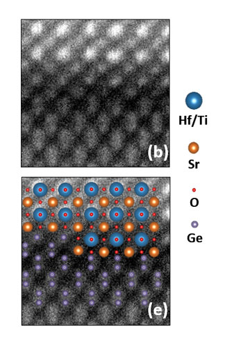
Previous work in our group showed that annealing temperature affected the interface trap density of SHO films. Films annealed at less than 650 °C retained an abrupt Ge–SHO interface. SHO annealed at 700 °C and 750 °C resulted in an interfacial layer evidenced by Ge XPS features that are suggestive of a hafnium germanide and a noncrystalline layer at the SHO–Ge interface.[ Reference McDaniel, Hu, Lu, Ngo, Posadas, Jiang, Smith, Yu, Demkov and Ekerdt 17 ] TEM and high-angle annular-dark-field (HAADF) analysis was performed on a 14-nm SrHf0.55Ti0.45O3 sample, which was grown with a subcycle ratio m:n = 3:1 using 11 supercycles. For this sample the Sr:Ti dosing ratio was 1:1 within subcycle n and this produced a film with Sr/(Sr + Hf + Ti) of 49%. A film with good thickness uniformity and surface smoothness is visible in Fig. 4(a). Figures 4(b) and 4(c) show HAADF STEM images of the SHTO–Ge interface and Fig. 5 shows enlargements from selected regions in Fig. 4(c). An abrupt interface without an obvious interfacial layer is found when the SHTO was annealed at 645 °C, which is consistent with previous work.[ Reference McDaniel, Hu, Lu, Ngo, Posadas, Jiang, Smith, Yu, Demkov and Ekerdt 17 ] EELS composition mapping was performed to investigate the element distribution across the interface. The EELS data presented in Supplementary Material Fig. S5 indicate that there is no interdiffusion across the Ge–SHTO interface and that the SHTO composition is spatially uniform.

Figure 4. Transmission electron micrographs of 14.0-nm SrHf0.55Ti0.45O3 with post-deposition annealing at 645 °C for 5 min: (a) TEM image showing the cross-sectional view of the SHTO film, (b) and (c) high-resolution HAADF STEM images showing details of the SHTO–Ge interface. In Figure (b), the full lines mn and nl indicate the Hf/Ti plane, the dotted line is the extension of mn. The included angle between nl and the dotted line is ~2.2°. Regions ![]() ,
, ![]() , and
, and ![]() in Figure (c) are selected for further analysis in Fig. 5.
in Figure (c) are selected for further analysis in Fig. 5.

Figure 5. HAADF STEM images (a), (b), and (c) showing enlarged portions of regions ![]() ,
, ![]() , and
, and ![]() in Fig. 4(c), respectively. (d), (e), and (f) HAADF STEM images with atomic structure overlaid for (a), (b), and (c), respectively.
in Fig. 4(c), respectively. (d), (e), and (f) HAADF STEM images with atomic structure overlaid for (a), (b), and (c), respectively.
Local grain tilting is apparent in Fig. 4(b). The solid lines mn and nl represent the Hf/Ti plane adjacent to the Ge (001) surface and the dotted line is an extension of line mn. The included angle indicates a local crystal tilt near the Ge surface of ~2.2°. Grain tilting can be caused by several factors, including lattice mismatch and the resulting film strain.[ Reference Jiang, Zhang, Yu and Lee 34 , Reference Foster, Li, Buckett, Miller, Baldo, Rehn, Bai, Guo, You and Merkle 35 ] The SrHf0.55Ti0.45O3 film is expected to be under compressive strain through the crystallization and cooling steps. During the transformation from amorphous into a crystalline film, nucleation likely occurs at the Ge–SHTO interface to produce the epitaxial film. The presence of a stepped surface with a step height of ~5.658/4 = 1.414 Å, as visible in Fig. 4(b) and Region 1 in Fig. 4(c), will impact the lateral area over which an epitaxial crystalline domain can grow before it encounters a step that is not commensurate with the SHTO step height.
An antiphase boundary (APB) is visible in Region 1 of Fig. 4(c) as illustrated in the enlargements in Figs. 5(a) and 5(d). One possible reason is that crystallites initiated on adjacent Ge regions extend laterally to intersect above the surface step leading to APB formation in the crystalline film.[ Reference Wu, Aoki, Posadas, Demkov and Smith 36 ] The Ge columns near the APB in Figs. 5(a) and 5(d) are misaligned with the Hf/Ti columns, which is consistent with APB observed for STO grown by MBE on Si(001).[ Reference Wu, Aoki, Posadas, Demkov and Smith 36 ] Since the misalignments can result in increased Ge−Sr bond length, dangling Ge bonds may also be formed. Both of the column misalignments and the possible Ge dangling bonds at the interface may contribute to the electrical trap states observed for SHO.[ Reference McDaniel, Hu, Lu, Ngo, Posadas, Jiang, Smith, Yu, Demkov and Ekerdt 17 ] Surface steps without the formation of an APB are also indicated in Figs. 5(b) and 5(e).
The enlarged images in Figs. 5(c) and 5(f) indicate that some Ge retains the 2 × 1 reconstruction present in the starting surface (Fig. S1) during ALD and annealing. The local interface structure in Figs. 5(b)/5(e) and 5(c)/5(f) is similar to that found for BaTiO3 deposited by MBE on a Ge (001) surface that first had ½-monolayer of Sr deposited to form a Zintl layer.[ Reference Fredrickson, Ponath, Posadas, McCartney, Aoki, Smith and Demkov 37 ] This might indicate that Sr orders at the Ge(001) surface during the initial ALD cycles to form a Zintl layer with Ge.
Electrical properties
The crystallization temperatures for 4-nm thick STO and SHO were around 510 and 640 °C, respectively.[ Reference McDaniel, Hu, Lu, Ngo, Posadas, Jiang, Smith, Yu, Demkov and Ekerdt 17 , Reference McDaniel, Ngo, Posadas, Hu, Lu, Smith, Yu, Demkov and Ekerdt 18 ] At 700 °C an interfacial layer forms at the Ge–SHO interface that is <0.5 nm thick. This interfacial layer may contribute to the D it values that were as low as 2 × 10¹²/cm2/eV for crystalline SHO and increased with higher annealing temperatures.[ Reference McDaniel, Hu, Lu, Ngo, Posadas, Jiang, Smith, Yu, Demkov and Ekerdt 17 ] To test the dielectric performance, the SrHf x Ti1−x O3 film with x = 0.55 was used to fabricate a MOS capacitor. The microstructure for this film revealed the presence of an APB in the near surface region and partial 2 × 1 reconstruction at the Ge–SHTO interface and these could be sources of interface trap states. The C–V and I–V curves are shown in Figs. 6(a) and 6(b), respectively. From Fig. 6(a), the capacitance achieves saturation at around 1.93 µF/cm2, corresponding to a relative dielectric constant of k ~ 30. The I–V measurement shows leakage current of 0.1 A/cm2 at 1 MV/cm with an EOT = 1.8 nm. The leakage current for SHO is 6.3 × 10⁻⁶ A/cm2 at 1 MV/cm with an EOT = 1.0 nm and for STO is 10 A/cm2 at 1 MV/cm with an EOT = 0.7 nm. Ignoring the EOT difference, which will cause even higher leakage current for this SrHf0.55Ti0.45O3 sample if it was considered, the leakage current of SHTO shows two orders of magnitude improvement over STO. However, the leakage current was too high to allow reliable D it to be measured.

Figure 6. Capacitance–voltage (C–V) measurement (a) and current–voltage (I–V) measurement (b) for a 14.0-nm SrHf x Ti1−x O3 (x = 0.55) film on Ge. The dielectric constant is k = 30 and the leakage current is 0.1 A/cm2 at 1 MV/cm with an EOT = 1.8 nm.
Conclusion
In this study, amorphous SrHf x Ti1−x O3 films have been grown on Ge (001) by ALD and annealed at 530 °C to 660 °C to crystallize the film into a heteroexpitaxial layer. Matching the lattice constant for the SHTO alloy with the substrate by adjusting x did not lower the SHTO crystallization temperature rather the crystallization temperature increased monotonically with increasing Hf content. In situ XPS and AR-XPS analysis verified the stoichiometry and uniformity of the grown films. The ex situ XRR, XRD and rocking curve measurements were used to determine the thickness, lattice constant and crystallinity, respectively. The interface of a selected sample was explored by STEM and EELS mapping. The interface was abrupt with no apparent interdiffusion between the substrate and the SHTO layer. Regions of the Ge surface retained the 2 × 1 reconstruction. Film defects included grain tilting and APBs that are attributed to steps at the Ge (001) surface. Capacitance–voltage (C–V) and current–voltage (I–V) measurements show the dielectric constant k = 30 and a leakage current I = 0.1 A/cm2 (at 1 MV/cm with EOT = 1.8 nm) after the standard MOS capacitor was fabricated from a 14.0-nm SHTO film with Hf content x = 0.55.
These results for SHTO films illustrate that ALD growth of quaternary perovskites directly on Ge (001) is feasible and that the properties can be adjusted with B-site substitution. Understanding the influence of strain and film microstructure on the D it for crystalline ABO3 layers on Ge necessarily requires systems that do not feature Ti on the B-site since Ti 3d states yield negligible conduction band offset with Ge, and require systems that crystallize at or below 650 °C to maintain an abrupt interface.
Supplementary Material
The supplementary material for this article can be found at http://dx.doi.org/10.1557/mrc.2016.36
Acknowledgments
This research was supported by the National Science Foundation (Award CMMI-1437050) and the Air Force Office of Scientific Research (Grant FA9550-14-1-0090).


