


Introduction
The performance improvement of large-scale integration (LSI) has progressed owing to the miniaturization of transistors. The degree of integration has increased following Moore's law, which predicted that the number of components in LSI would doubles every 2 years.[Reference Moore1, Reference Moore2] This prediction has surprisingly come true since—the semiconductor industry has made constant efforts to continue satisfying the law. The increase in the number of transistors has been directly linked to the growth of computing performance, and such continuous improvement of computing performance has been realized over the last 70 years.
Koomey et al. examined the strong correlation between computing performance and power efficiency of computation.[Reference Koomey, Berard, Sanchez and Wong3] Their work showed that the improvement of power efficiency is essential for the improvement of computing performance. From the perspective of electronic devices, the improvement of power consumption of transistors paved the way to increase the available number of transistors with a limited power supply, which resulted in the successful improvement of computing performance. In other words, low-power consumption is the essence of transistor miniaturization. This has enabled us to realize outstanding applications such as notebook personal computers, smartphones, tablets, and so on.
Dennard scaling guided the miniaturization of metal–oxide–semiconductor field-effect transistors (MOSFETs), which are the building blocks of contemporary LSIs.[Reference Dennard, Gaensslen, Rideout, Bassous and LeBlanc4] Dennard scaling provides guidelines to reduce the power consumption of MOSFETs with device-size miniaturization. However, Dennard scaling is not valid any longer for the state-of-the-art MOSFETs, because of short-channel effects.[Reference Taur and Ning5] However, the semiconductor industry has achieved both miniaturization and the reduction of power consumption after the era of Dennard scaling, in which the key technologies were finFETs,[Reference Hisamoto, Lee, Kedzierski, Takeuchi, Asano, Kuo, Anderson, King, Bokor and Fu6] SOI-FETs,[Reference Kuhn7] and high-k technology[Reference Robertson8] to enhance electrostatic gate control. In the current situation, the scaling law seems to have been prolonged, but some new technologies have realized miniaturization and low-power consumption together.
Now, we are at the last stage of miniaturization. However, the enhancement of computing performance is still a demand because of new applications such as machine learning and artificial intelligence. In this situation, the reduction of power consumption must be continued even if miniaturization has been completed.
An approach to reduce the power consumption without miniaturization is the use of steep slope devices (SSDs) as new building blocks for LSIs instead of MOSFETs. SSDs can realize much steeper switching from the OFF to ON state, resulting in decreasing voltage for switching. MOSFETs have a physical limit that the subthreshold swing (SS) cannot be < 60 mV/decade at 300 K.[Reference Sze9] SSDs can operate with an SS < 60 mV/decade; thus, they can operate at a lower voltage compared with the operating voltage of MOSFETs, resulting in low-power consumption. Some existing candidates for SSDs are tunnel field-effect transistors (TFETs),[Reference Seabaugh and Zhang10] negative capacitance FETs,[Reference Salahuddin and Datta11] and threshold switches.[Reference Shukla, Grisafe, Ghosh, Jao, Aziz, Frougier, Jerry, Sonde, Rouvimov, Orlova, Gupta and Datta12]
This paper concerns TFETs, which are a type of gated p–i–n diodes and have MOSFET-like structures in which the source and drain show different types of conduction. In TFETs, the tunnel barrier is a pn junction at the source side edge of the gate. The gate electrostatic control regulates tunneling current flowing through the barrier by changing the thickness of the pn junction, which enables TFETs to realize steeper switching compared with that of MOSFETs. Stuetzer's and Shockley's experiments have formed the foundation of TFET-like devices.[Reference Stuetzer13, Reference Schockley and Hopper14] Modern TFETs having the MOS structure were proposed by Quinn et al.[Reference Quinn, Kawamoto and McCombe15] and independently demonstrated by Baba.[Reference Baba16] Appenzeller et al. first demonstrated sub-60 mV/decade operation using a carbon-nanotube TFET.[Reference Appenzeller, Lin, Knoch and Avouris17] Choi et al. first demonstrated sub-60 mV/decade operation in Si-TFETs.[Reference Choi, Park, Lee and King Liu18] Since then, many research groups have reported sub-60 mV/decade operation of Si-TFETs.[Reference Kim, Kam, Hu and King Liu19–Reference Mori, Yasuda, Fukuda, Morita, Migita, Tanabe, Maeda, Mizubayashi, O'uchi, Liu, Masahara, Miyata and Ota24]
The low ON current (I ON) is the most significant issue in TFET research. The I ON of TFETs is still not sufficient for practically fast circuit operation. TFETs inherently have a high-resistance tunneling barrier. As the tunneling current is essentially related to material science, many TFETs with new materials, including not only Ge or III–V materials[Reference Takagi, Ahn, Noguchi, Gotow, Nishi, Kim and Takenaka25] but also two-dimensional semiconductors,[Reference Li, Yan, Jena and Xing26] have been reported. Recently, a material engineering technique to enhance tunneling current in Si has been proposed, which utilizes isoelectronic traps (IETs),[Reference Mori, Morita, Miyata, Migita, Fukuda, Masahara, Yasuda and Ota27, Reference Mori, Morita, Miyata, Migita, Fukuda, Mizubayashi, Masahara, Yasuda and Ota28] Experimental demonstrations of the current enhancement and improvement of circuit performance have been reported,[Reference Mori, Morita, Miyata, Migita, Fukuda, Masahara, Yasuda and Ota27, Reference Mori, Asai, Hattori, Fukuda, Otsuka, Morita, O'uchi, Fuketa, Migita, Mizubayashi, Ota and Matsukawa29] in which IET-assisted tunneling (IETT) is utilized instead of conventional band-to-band tunneling (BTBT).
This paper reviews the IET technology to enhance I ON in Si-TFETs. General issues concerning TFETs have been reviewed in.[Reference Seabaugh and Zhang10, Reference Ionescu and Riel30] First, we present an overview of the state-of-the-art TFET research. Then, we examine the IET technology for Si-TFETs.
Overview of state-of-the-art TFET research
Guidelines to enhance BTBT
Before starting to discuss IET technology, we briefly discuss the conventional guidelines to improve TFET performance, aiming to summarize the background of the IET technology.
BTBT through a pn junction is categorized as Esaki tunneling under a forward bias or as Zener tunneling under a reverse bias. TFETs utilize Zener tunneling [Fig. 1(a)]. We begin with the equation of tunneling current flowing through a junction sandwiched between two electrodes[Reference Datta31]:
 $$I \propto \mathop \int \nolimits \left[ {\,f_1 \left( E \right) - f_2 \left( E \right)} \right]\left \vert M \right \vert ^2 D_1 \left( E \right)D_2 \left( E \right)dE, $$
where f(E) is a Fermi function, M is a transfer matrix element for transition, and D(E) is a density-of-state (DOS) function. Tunneling is a transition between two states. Thus, M can be expressed following Fermi's golden rule as
 $$\left \vert M \right \vert ^2 \,\propto\, \left \vert {\langle\psi _2 {\rm \vert} \!\!-\!\!Fx{\rm \vert} \psi _1\rangle} \right \vert ^2, $$
where ψ is a wave function and the perturbative transition Hamiltonian is –Fx, in which F is the strength of the electric field at the junction, and x is the electron coordinate along the tunneling direction. In the case of BTBT through a pn junction, ψ 1 is the state of valence band maximum (VBM), and ψ 2 is that of conduction band minimum (CBM).
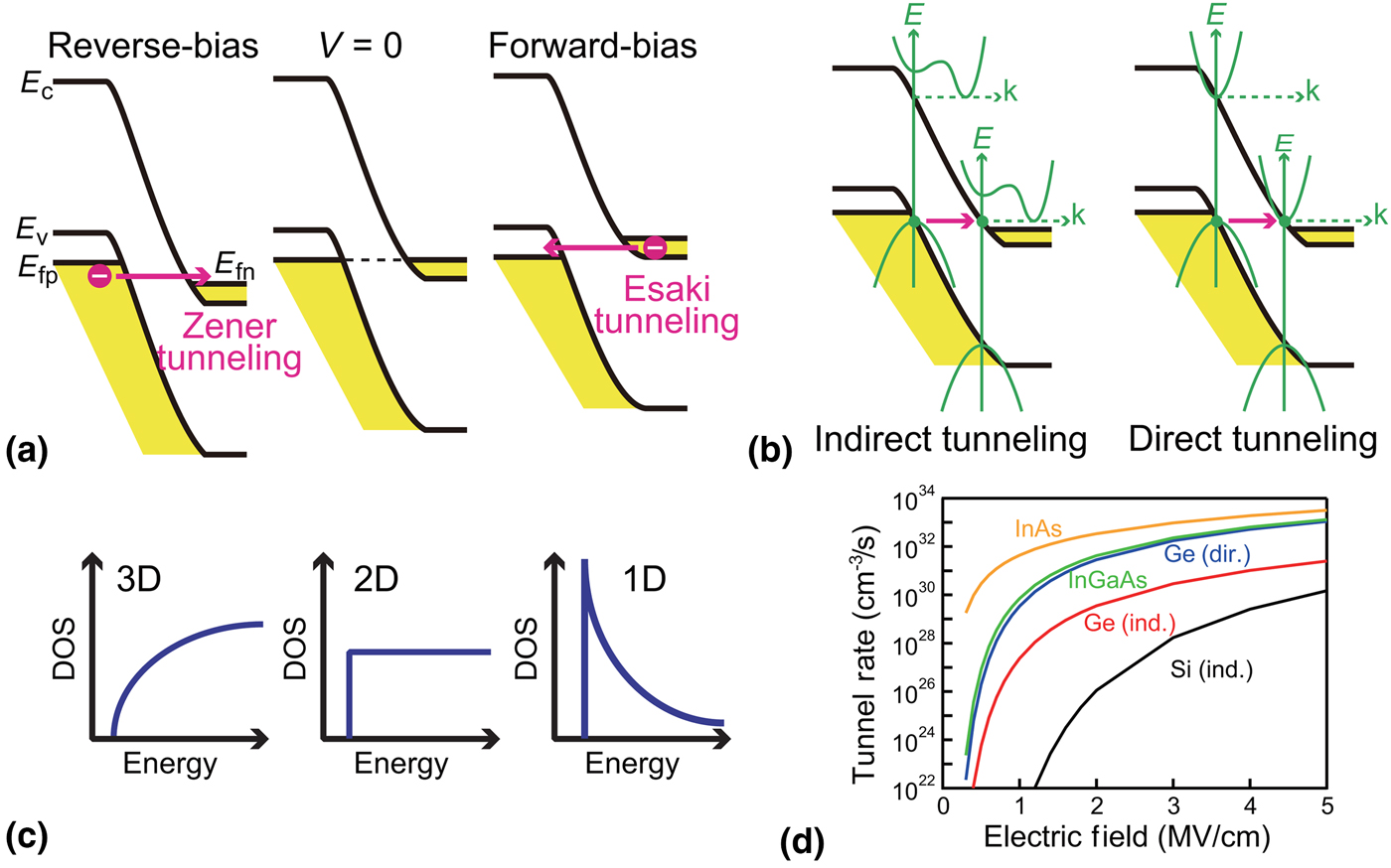
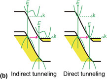
Figure 1. (a) Schematic band diagrams for a pn diode. (b) Schematic views of indirect and direct processes for Zener tunneling. The E–k relationship is superimposed on band diagrams. (c) Density of states for free electrons in 3D, 2D, and 1D systems. (d) Tunneling rates for typical semiconductors calculated with Eqs. (3)–(5).
Equation (2) provides the first guideline to enhance tunneling current in TFETs: we should aim to increase the value of the integral on the right-hand side of the equation. Among conventional semiconductor materials used in electronic devices, which have crystal structures such as diamond, zincblende, and wurtzite, direct-band gap semiconductors, such as InGaAs, have a p-like VBM state and an s-like CBM state. Here the integral on the right-hand side of Eq. (2) has a significant value. In contrast, indirect-gap semiconductors, such as Si, have p-like CBM and VBM states, because of which the integral on the right-hand side has an insignificant value [Fig. 1(b)]. In indirect-gap semiconductors, as in the case of luminescence, phonon-assisted indirect tunneling occurs; however, its transition probability is lower than that of direct tunneling. This situation can be understood as the wave-number conservation rule. However, the indirect Ge case, in which direct tunneling occurs because the direct gap energy is close to the indirect gap energy, is complicated.[Reference Kao, Verhulst, Vandenberghe, Sorée, Groeseneken and De Meyer32] The direct/indirect tunneling current can be experimentally distinguished by temperature-dependent electric measurements.[Reference Mori, Morita, Miyata, Migita, Fukuda, Mizubayashi, Masahara, Yasuda and Ota28]
The second guideline is related to DOS, as expressed in Eq. (1). A higher DOS results in a higher tunneling current. Furthermore, the DOS depends on the dimensionality of a system, which affects SS [Fig. 1(c)]. For example, the step function of the DOS in two-dimensional (2D) systems leads us to expect steeper switching than in the corresponding three-dimensional (3D) case.[Reference Lattanzio, De Michielis and Ionescu33–Reference Agarwal, Teherani, Hoyt, Antoniadis and Yablonovitch35] This is also valid in one-dimensional (1D) systems. Thus, low-dimensional systems like 2D semiconductors or nanowires have an advantage in terms of SS in addition to electrostatic control, as expected in MOSFETs.
Kane derived a familiar equation for Zener's BTBT,[Reference Kane36] which yields the third guideline. The equation for tunneling rate G, which is proportional to I, is expressed as[Reference Kao, Verhulst, Vandenberghe, Sorée, Groeseneken and De Meyer32, Reference Kane36]
 $$G = AF^P {\rm exp}\left( { - \displaystyle{B \over F}} \right),$$
where A and B are Kane tunneling parameters, and P is 2 and 2.5 for direct and indirect BTBT, respectively. In the case of direct BTBT, the Kane tunneling parameters are
 $$A = \displaystyle{{gm_{\rm r}^{1/2} q^2} \over {\pi h^2 E_{\rm g}^{1/2}}}, $$
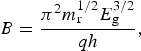 $$B = \displaystyle{{\pi ^2 m_{\rm r}^{1/2} E_{\rm g}^{3/2}} \over {qh}},$$
where g is a degeneracy factor, m r is the tunnel mass (1/m r = 1/m c + 1/m v, where m c and m v are the effective masses for conduction and valence bands, respectively), and E g is the band gap energy. According to Eqs. (3) and (5), a smaller B results in a higher tunneling current. Then, according to Eq. (5), we can expect a higher tunneling current with smaller E g and m r. Qualitatively speaking, m c is proportional to E g[Reference Harrison37]; therefore, we can choose materials having both a small E g and small m r. However, materials with a smaller effective mass have a smaller DOS.[Reference Davis38] Because of this trade-off relationship, a balance between E g and m r, as expressed in Eq. (4), is required. Figure 1(d) shows a plot of G versus F calculated using Eqs. (3)–(5) for typical semiconductor materials. It is noted that the OFF current in TFETs increases with decreasing E g because of the lower tunneling barrier, although here we discuss I ON and SS only.
As discussed above, the guidelines to obtain a higher tunneling current are the utilization of direct-gap semiconductors with lower E g (so as to not increase the OFF current) and low-dimensional device structures.
Device demonstrations
To our knowledge, the best performance thus far was reported in Lund University for an N-type nanowire TFET, in which an InAs/GaAsSb heterojunction was utilized.[Reference Kane36] The device exhibited I on = 10 µA/μm and SS = 48 mV/decade at V DS = 0.3 V. The device follows the guidelines discussed in the previous section.
Figure 2(a) shows a benchmark for experimentally demonstrated N-type TFETs. III–V TFETs exhibit higher I ON values. The benchmark follows the guidelines discussed in the previous section. For Ge-TFETs, which can utilize direct tunneling, the highest performance reported thus far was achieved in Tokyo University.[Reference Harrison37] The highest SS of 21 mV/decade was achieved in Hokkaido University with InAs/Si heterojunction nanowire TFETs.[Reference Davis38] For Si-TFETs, two devices showing better performance have been reported[Reference Choi, Park, Lee and King Liu18, Reference Huang, Zhan, Huang, Mao, Zhang, Qiu and Wang51]; however, because these two devices were operated with a relatively high operation voltage, we cannot compare them with the devices shown in this benchmark.
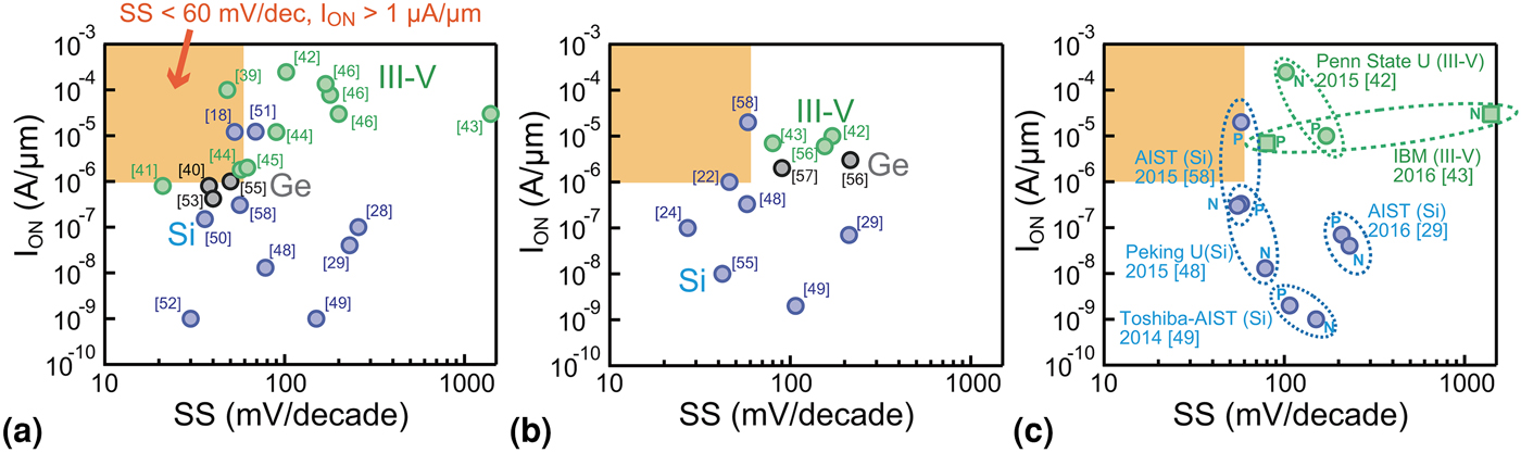
Figure 2. Benchmark plots for (a) N-type and (b) P-type TFETs. (c) A plot for a limited number of samples realizing integration.
Some discussions are required on P-type TFETs. Figure 2(b) shows a benchmark for P-type TFETs. Surprisingly, Si-TFETs, which are expected to show poor performance because of indirect tunneling, exhibits better performance than III–V and Ge TFETs. This is probably because it is difficult to fabricate the source–channel junction for P-type TFETs with III–V materials or Ge, for which the source is n-type and the channel is p-type. At present, we do not have a solution for this problem, but some articles discussed the feasibility of realizing P-type TFETs with these materials.[Reference Pandey, Schulte-Braucks, Sajjad, Barth, Ghosh, Grisafe, Sharma, von den Driesch, Vohra, Rayner, Loo, Mantl, Buca, Yeh, Wu, Tsai, Antoniadis and Datta56]
Recently, some papers reported the experimental demonstration of TFET integration. Six papers reported the fabrication of both types of TFETs on the same wafer. A benchmark limited to these six papers is shown in Fig. 2(c). Of these, two papers utilized III–V TFETs,[Reference Pandey, Madan, Liu, Chobpattana, Barth, Rajamohanan, Hollander, Clark, Wang, Kim, Gundlach, Cheung, Suehle, Engel-Herbert, Stemmer and Datta42, Reference Cutaia, Moselund, Schmid, Borg, Olziersky and Riel43] and the other four utilized Si-TFETs.[Reference Mori, Asai, Hattori, Fukuda, Otsuka, Morita, O'uchi, Fuketa, Migita, Mizubayashi, Ota and Matsukawa29, Reference Huang, Jia, Chen, Zhu, Guo, Wang, Wang, Wu, Wang, Bu, Kang, Wang, Wu, Lee, Wang and Huang48, Reference Kondo, Goto, Morita, Mori, Migita, Hokazono, Ota, Masahara and Kawanaka49, Reference Morita, Mori, Migita, Mizubayashi, Fukuda, Matsukawa, Endo, O'uchi, Liu, Masahara and Ota58] Si-TFETs show good performance owing to the ease of integration. The guidelines for TFET development are as discussed in the previous section; however, there remain difficulties in satisfying all the guidelines.
Isoelectronic trap (IET) technology
Concept
For taking advantage of the ease of integration of Si-TFETs, we aim to enhance I ON in Si-TFETs sufficiently for practical application. However, the BTBT rate in Si-TFETs is low in principle. A new idea to enhance I ON in Si-TFETs is to utilize a tunneling path different from BTBT, and Mori et al. proposed the use of IET technology.[Reference Mori, Morita, Miyata, Migita, Fukuda, Masahara, Yasuda and Ota27, Reference Mori, Morita, Miyata, Migita, Fukuda, Mizubayashi, Masahara, Yasuda and Ota28] The proposal is to produce an intermediate isolated state in the pn junction and utilize the tunneling current mediated by the state [Fig. 3(a)]. The intermediate state acts as a “stepping stone” for electrons tunneling from the valence to conduction bands. Thus, we can realize a tunneling path different from BTBT. In this idea, the key point is the concentration of the intermediate state. The concentration should be sufficiently low such that the intermediate state is isolated and does not form a band. In this situation, the intermediate state is not selective in terms of wave numbers, like atoms. In other words, the intermediate state can take any wave number because of the uncertainty principle. Following this scenario, we can aim to relax the k-conservation rule in indirect-gap semiconductors and realize pseudo-direct tunneling to obtain a higher tunneling rate. Here isoelectronic impurities (IEIs) are chosen to form the intermediate state. Specifically, the Al–N pair is chosen, as discussed later.
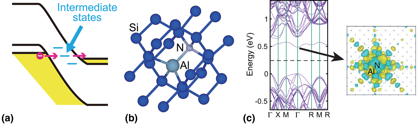
Figure 3. (a) Schematic representation showing the idea of using intermediate states for tunneling through a pn junction. (b) Schematic atomic configuration of an Al–N pair in a host Si crystal. (c) Calculated band diagram of Si with an Al–N pair. The Al–N pair provides a discrete state in the band gap. The wave function of the discrete state at the Γ point is also shown.
Isoelectronic impurities
There is a long history of research on IEIs, which have been mentioned in papers published in the 1960s. IEIs are also called “isovalent electron impurities” because the impurities are isovalent with the host material and do not produce carriers. In the simplest substitutional view, for Si, other group-IV elements such as C, Ge, and Sn can be IEIs. The impurity pairs following the octet rule, such as III–V and II–VI pairs, are also IEIs if they do not produce dangling bonds. The definition as not producing carriers is notably wide, but the IEIs of interest form states in the band gap of host materials and produce unique physical phenomena such as luminescence. The mechanisms for the formation of states by IEIs have been discussed previously.[Reference Brown, Hall and Lockwood59] There are two scenarios: one is that the core charge, different from that of the host material, provides strong short-range potential perturbation, while the other is that the atom-size difference between the IEIs produces local strains resulting in potential perturbation in the host material.
Thus far, the most successful application of IEIs has been green light-emitting diodes (LEDs) realized using GaP:N before the InGaN era. GaP is an indirect-gap host material.[Reference Thomas and Hopfield60] The IEI in this application is N, which forms N–N pairs in the host GaP and realizes strong pseudo-direct luminescence at room temperature. Specifically, the luminescence originates from the exciton emission bound to the IET.
Isoelectronic impurities in silicon
The IEIs in Si have also been studied with the motivation to realize LEDs. Unfortunately, the binding energy of excitons bound to IET states is not sufficient for emission at room temperature, because of which its practical application has not been realized yet. The situation of IETs in Si is slightly complicated. The substitutional C, Ge, and Sn—the previously called “simple” IEIs—do not exhibit the exciton emission bound to the IETs. It is supposed that these IEIs do not yield the important states in the band gap. The IET emissions were observed with single-atom IEIs, which are In,[Reference Thewalt, Ziemelis and Parsons61] Be,[Reference Henry, Lightowlers, Killoran, Dunstan and Cavenett62] Cu,[Reference Weber, Bauch and Sauer63] S,[Reference Brown and Hall64] Se,[Reference Bradfield, Brown and Hall65] and Zn,[Reference Henry, Campion and McGuigan66] and an atom-pair IEI, which is Al–N.[Reference Modavis and Hall67] The single-atom IEIs contain donor/acceptor impurities. For Zn, for example, it is suggested that Zn–O pairs are produced with residual O impurities in Si substrates.[Reference Daly, McGlynn, Henry, Campion, McGuigan, do Carmo and Nazaré68] For Be, the IET is produced by Be–Be pairs.[Reference Brown, Bradfield, Hall and Soref69] For In, it is suggested that residual N atoms in Si substrates cause the IET formation.[Reference Brown, Hall and Lockwood59]
There are a relatively large number of papers on the Al–N IEI, and we utilized the Al–N IEI for our works. First, Weber et al. experimentally investigated emissions observed in Si:Al in detail; then, they suggested that the IETs in Si:Al were produced by a substitutional pair having C3v symmetry along the 〈111〉 axis.[Reference Weber, Schmid and Sauer70] Subsequently, Alt and Tapfer revealed that N atoms participate in these emissions,[Reference Ch. Alt and Tapfer71] and Modavis and Hall realized strong luminescence by the co-doping of Al and N.[Reference Modavis and Hall67] Moreover, Tajima and Kamata utilized these emissions to estimate the residual N concentration in Si wafers.[Reference Tajima and Kamata72] The IET state is approximately 30 meV below the CBM.[Reference Weber, Schmid and Sauer70] The most recent studies were conducted by Iizuka and Nakayama using first-principles calculations.[Reference Iizuka and Nakayama73, Reference Iizuka and Nakayama74] They clarified the stable atomic configuration of the Al–N pair: the substitutional nearest-neighbor configuration is preferred over configurations comprising interstitials [Fig. 3(b)]. This configuration follows the prediction of Weber et al. based on their experiments. The Al–N pair provides a state in the band gap, which mainly comprises the N 3s state [Fig. 3(c)].[Reference Iizuka and Nakayama73]
Proof-of-concept experiments
On diodes
In this section, we discuss the enhancement of tunneling current flowing in diodes under the reverse-bias condition resulting from the introduction of an IEI, which was the first proof-of-concept experiment.[Reference Mori, Morita, Miyata, Migita, Fukuda, Masahara, Yasuda and Ota27, Reference Mori, Morita, Miyata, Migita, Fukuda, Mizubayashi, Masahara, Yasuda and Ota28] The diode consisted of an n-type epitaxial Si thin film on a p-type substrate [Fig. 4(a)]. The Al–N IEI was doped by the ion implantation (I/I) processes and activated by low-temperature annealing at 450°C. The formation of the IET state was confirmed by photoluminescence spectroscopy at cryogenic temperature. The concentrations of Al and N were approximately 1018 cm−3 around the pn junction. Four types of diodes were examined: Al–N-, Al-, and N-implanted diodes and a control diode without additional impurities [Fig. 4(b)]. The temperature dependence of tunneling current in the control diode follows the trend of conventional indirect BTBT.[Reference Mori, Morita, Miyata, Migita, Fukuda, Mizubayashi, Masahara, Yasuda and Ota28] In the higher temperature range, the tunneling current flowing in the implanted diodes comprises the so-called trap-assisted tunneling (TAT) consisting of tunneling to an impurity or defect state and thermal emission from the state to the band. Therefore, it is fair to compare such currents with currents in the lower temperature range, in which tunneling consists of “pure” tunneling without thermal paths. In the comparison, the Al–N-implanted diode exhibited a current enhancement by a factor of 735, which implies that the Al–N co-doping enhances the tunneling current. The Al-implanted diode also exhibited current enhancement, but the enhancement was less than that in the Al–N case and is probably similar to the case of Tajima's experiments,[Reference Tajima and Kamata72] in which the residual N impurity in a Si wafer causes the Al–N formation. The N-implanted diode exhibited no enhancement, but the current decreased because I/I defects are likely to compensate for carrier-generating dopants making the junction less steep. The current enhancement does not originate from the change of carrier concentration accompanying Al and N doping. The co-doping of Al and N induces hole generation in Si, and its activation ratio is approximately 10%.[Reference Mori75] Therefore, the change of carrier concentration does not significantly affect tunneling current.
Figure 4. (a) Schematic representation of diodes fabricated in Refs. Reference Mori, Morita, Miyata, Migita, Fukuda, Masahara, Yasuda and Ota27 and Reference Mori, Morita, Miyata, Migita, Fukuda, Mizubayashi, Masahara, Yasuda and Ota28. (b) Temperature dependence of four types of diodes.[Reference Mori, Morita, Miyata, Migita, Fukuda, Mizubayashi, Masahara, Yasuda and Ota28] (c) Summary of tunneling paths in IET-assisted diodes.[Reference Mori, Morita, Miyata, Migita, Fukuda, Mizubayashi, Masahara, Yasuda and Ota28]
The above experiment was the first to show that the co-doping of Al and N enhances the tunneling current in Si. The supposed tunneling paths are summarized in Fig. 4(c). From this demonstration, it is not certain what IETT is—it will be discussed later with the results of a theoretical calculation.
On TFETs
The next experiment was on TFETs,[Reference Mori, Morita, Miyata, Migita, Fukuda, Masahara, Yasuda and Ota27, Reference Mori, Migita, Fukuda, Asai, Morita, Mizubayashi, Liu, O'uchi, Fuketa, Otsuka, Yasuda, Masahara, Ota and Matsukawa76] which demonstrated N-type TFETs on a silicon-on-insulator (SOI) wafer. The high-k/metal gate technology was also utilized [Fig. 5(a)]. The I–V characteristics at room temperature are shown in Fig. 5(b). The I d − V d curves exhibit I ON enhancement by a factor of 11 owing to the doping of Al–N. The SS was also improved owing to the current enhancement, as expected from Eq. (3). These improvements were also observed at a cryogenic temperature, as in the diode case. The I OFF slightly increased because of the increase of tunneling current flowing through the junction at the drain side. This is not essential for the IET technology. If we utilize the so-called drain-offset structure,[Reference Mori, Yasuda, Maeda, Mizubayashi, O'uchi, Liu, Sakamoto, Masahara and Ota77] we can avoid the I OFF increase despite utilizing IET technology.[Reference Mori, Mizubayashi, Morita, Migita, Fukuda, Miyata, Yasuda, Masahara and Ota78] Unfortunately, the enhancement is less than that of diodes, which is supposed to be related to the mechanism of IETT, as discussed later. The entire active region consisting of the source, channel, and drain was exposed by Al–N I/I in the experiments. Then, the source sheet resistance was increased with I/I,[Reference Mori, Morita, Miyata, Migita, Fukuda, Masahara, Yasuda and Ota27] which suggests that Al–N implantations compensate for carrier-generating dopants, as is the case with N implantation in the diodes.
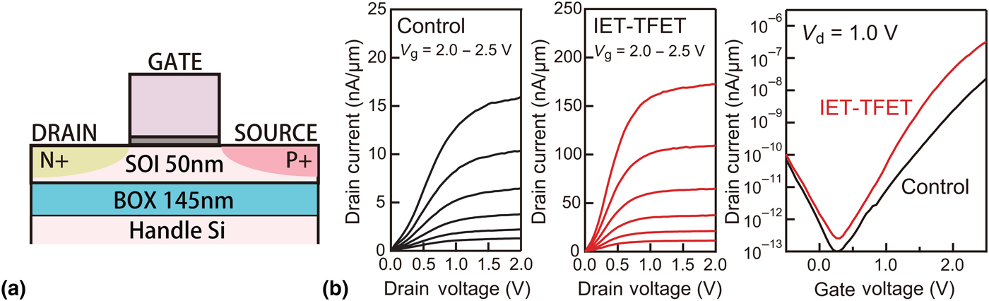
Figure 5. (a) Schematic representation of an N-type TFET fabricated on an SOI wafer.[Reference Mori, Morita, Miyata, Migita, Fukuda, Masahara, Yasuda and Ota27] (b) I–V curves of the control TFET, which does not incorporate IET, and IET–TFET.[Reference Mori, Morita, Miyata, Migita, Fukuda, Masahara, Yasuda and Ota27]
Another experiment has been conducted utilizing heated ion implantation (HII),[Reference Mori, Mizubayashi, Morita, Migita, Fukuda, Miyata, Yasuda, Masahara and Ota78] which is used to reduce implantation defects by heating the wafer when I/I is performed. In the experiment, the wafer was heated to 200°C in the Al and N implantation processes. The HII process realized an I ON value three times that of the conventional IET–TFET with the RT I/I process. A lower number of I/I defects result in stronger IET effects. The comprehensive scenario is as follows. The defects hamper the IET activation. Fewer defects increase active IET and result in the greater current enhancement. It is supposed that the current enhancement with IET notably concerns the microscopic structure surrounding Al–N pairs.
On TFET circuits
The final objective of I ON enhancement is faster circuit operation. Complementary TFET (CTFET) circuit operation has been demonstrated with the IET technology.[Reference Mori, Asai, Hattori, Fukuda, Otsuka, Morita, O'uchi, Fuketa, Migita, Mizubayashi, Ota and Matsukawa29] The experiment was slightly different from the experiments in the previous section. I ON enhancement by factors of five and two has been achieved in P- and N-type TFETs, respectively [Fig. 6(a)]. The simplest CTFET circuit is an inverter, as shown in Fig. 6(b). A higher gain was achieved, especially in a low operation-voltage range, owing to the I ON enhancement. The full swing was not achieved because of the high I OFF, which can be avoided by using the drain-offset structure simulated as an orange curve in Fig. 6(b). The situation seems to be the case in the previous section.
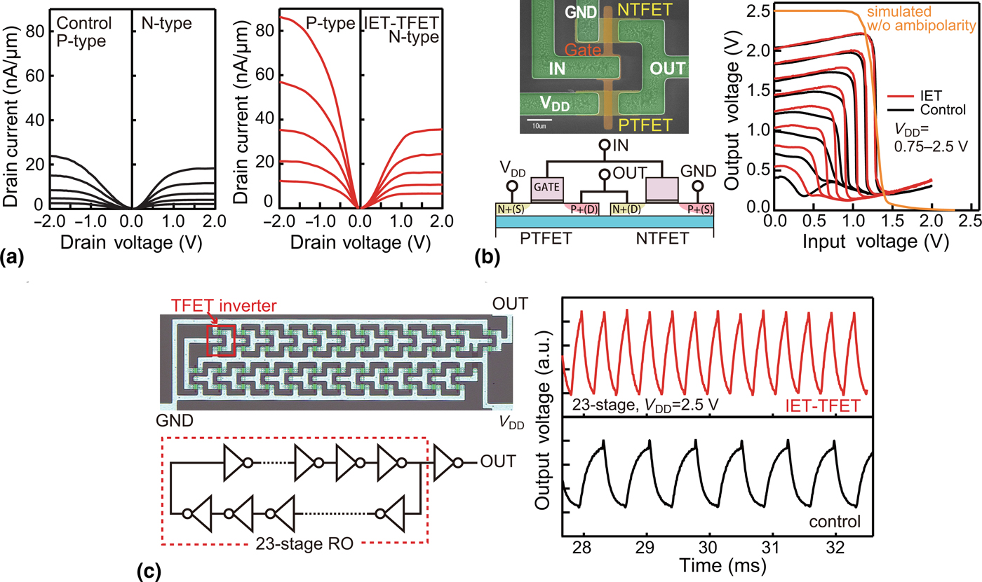
Figure 6. (a) I D − V D curves of P- and N-type TFETs. The IET technology enhances tunneling current.[Reference Mori, Asai, Hattori, Fukuda, Otsuka, Morita, O'uchi, Fuketa, Migita, Mizubayashi, Ota and Matsukawa29] (b) SEM image, schematic structure, and transfer curves of TFET inverters.[Reference Mori, Asai, Hattori, Fukuda, Otsuka, Morita, O'uchi, Fuketa, Migita, Mizubayashi, Ota and Matsukawa29] (c) Optical microscope image, schematic circuit diagram, and output waveforms of 23-stage full TFET ring oscillators.[Reference Mori, Asai, Hattori, Fukuda, Otsuka, Morita, O'uchi, Fuketa, Migita, Mizubayashi, Ota and Matsukawa29]
The ring oscillator (RO) circuit is fabricated to estimate circuit operation speed, which is the first performance indicator for newly developed devices. Twenty-three-stage full TFET ROs, in which all transistors were TFETs, were fabricated and successfully operated [Fig. 6(c)].[Reference Mori, Morita, Miyata, Migita, Fukuda, Masahara, Yasuda and Ota27] The output waveforms are also shown in the figure. It is clear that the IET technology enhances operation speed owing to the current enhancement. It is noted that this was the first demonstration of RO circuit operation for TFETs.
Theoretical view of IETT
Iizuka et al. reported the theoretical framework of IETT.[Reference Iizuka, Asayama and Nakayama79] This section is based on their paper. Figure 7(a) shows the tunneling path of IETT. Electron tunneling occurs in path A, which has a long distance. It is assumed that electrons move in path B by drift transport because the IET state resonates with the CB state. We find that the assumption is correct later. It is noted that IETT does not include thermal paths; therefore, it is expected that IETT exhibits no temperature dependence like TAT, which includes a thermal transition path. On the other hand, the experiments showed a temperature dependence of SS. It was probably caused by TAT originating from defects in the junction, which are not an essential characteristic of IETT.[Reference Mori, Morita, Miyata, Migita, Fukuda, Masahara, Yasuda and Ota27]
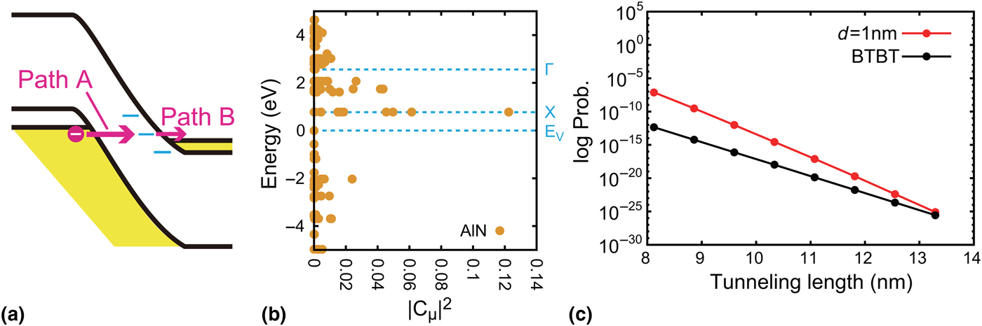
Figure 7. (a) Tunneling of IETT consisting of two paths: the longer path A and the shorter path B. (b) Plot of components of ψ IET decomposed by wave functions of host Si, φ Si,μ, as a function of eigenenergy, where |C μ|2 = |〈ψ IET|ϕ Si,μ〉|2.[Reference Iizuka, Asayama and Nakayama79] (c) Tunneling probability of BTBT and IETT. The length of path B is assumed as d = 1 nm.[Reference Iizuka, Asayama and Nakayama79]
According to Eq. (1), we should first consider DOS. The DOS of the VBM and CBM were estimated as D v = 1.19 × 10¹⁰ eV−1 and D c = 8.16 × 10⁹ eV−1, respectively. In contrast, the DOS of the IET state was liberally estimated as D IET = 3.25 × 10⁷ eV−1 under the assumption that all Al and N atoms formed activated pairs in the host material. As D IET is two orders of magnitude less than D c, |M|2 must compensate for the shortage to realize a higher current.
Two factors are involved in the enhancement of |M|2. One is tunneling length. The effective tunneling length of IETT is the length of path A shown in Fig. 7(a), which is clearly shorter than the length of BTBT, resulting in a larger |M|2. Here, we consider path B in which electrons move by drift transport as assumed in the first part of this section. Figure 7(b) shows a plot of components of ψ IET decomposed by the wave functions of host Si as a function of eigenenergy. The IET state mainly comprises X-point-like states. This indicates that the IET state resonates with the CBM state of host Si, because of which path B does not contribute to tunneling and IETT takes advantage of the shorter tunneling length. The other factor is the relaxed k-conservation rule. Figure 7(b) also shows that the variety of components is notably significant, which indicates that the IET state is localized and can relax the k-conservation rule along the tunneling direction. In relation to this, it is also important that the probability of BTBT in silicon is lower because of p-to-p transition as discussed previously, while the probability of IETT is higher because of p-to-s transition owing to the N-3s orbital nature of the IET state as discussed with Fig. 3(c). These two factors, tunneling length and relaxed k-conservation rule, enhance |M|2 to enhance tunneling current, despite the lower DOS.
Figure 7(c) shows the tunneling probability as a function of tunneling length. Both BTBT and IETT show the same trend of exponential increase with decreasing length. Here, we point out the difference of slope between these two curves. This difference is due to the difference of envelope function, and it indicates that a shorter tunneling length can realize a much higher enhancement ratio between IETT and BTBT. That is, if we realize a much shorter tunneling length—through device-structure modification, for example—we can expect a higher I ON in Si-TFETs. Furthermore, it is speculated that this causes the difference of enhancement ratio between the diodes and TFETs in the experiments. This fact is notably promising for Si-TFETs because we can expect a higher I ON than in the proof-of-concept experiments.
Summary and future outlook
In summary, we reviewed the IET technology proposed to enhance I ON in Si-TFETs. The proof-of-concept experiments demonstrated an I ON enhancement in SOI-TFETs by a factor of approximately 10. Theoretical calculation predicts that it is possible to realize a much higher I ON enhancement.
Here we comment on certain features of TFETs not mentioned in the main text. The fabrication process of Si-TFETs is compatible with that of conventional Si-MOSFETs; therefore, the fabrication cost does not matter. The scalability is expected to be better than that of MOSFETs because the short-channel effect is supposed to be insignificant in TFETs, the major characteristics of which are determined by the source-side edge of the gate. Therefore, in principle, planar-type TFETs could operate even in the technology node in which finFETs are utilized. The most important issue in the fabrication is source/drain formation because the self-alignment process of the source and drain for TFETs is not clear at present, which could hamper dimensional scaling. The performance variability is also under research. Especially for IET–TFETs, we can speculate that the IET impurities provide additional variation. On the other hand, it was reported that IET–TFETs exhibited less variation than conventional TFETs in the case of large devices, which is attributed to the decrease of tunneling rate fluctuation with the increase of tunneling probability.[Reference Mori, Migita, Fukuda, Asai, Morita, Mizubayashi, Liu, O'uchi, Fuketa, Otsuka, Yasuda, Masahara, Ota and Matsukawa76] Smaller IET–TFETs could exhibit much larger variation because of impurity fluctuation; however, there is a trade-off relationship between the increase of impurity fluctuation and the suppression of tunneling rate fluctuation. More research is needed to discuss the variability of IET–TFETs in detail.
Finally, we present an estimation of the future performance of IET–TFETs by utilizing simulations.[Reference Mori, Asai, Hattori, Fukuda, Otsuka, Morita, O'uchi, Fuketa, Migita, Mizubayashi, Ota and Matsukawa29] The enhancement in Si-TFET was assumed to be as high as in the case of the diodes; that is, enhancement by a factor of 735 was assumed. Here, not only I ON enhancement but also threshold-voltage optimization and device miniaturization to reduce capacitance were considered. The target operation voltage is approximately 0.3 V, at which MOSFETs show subthreshold operation.[Reference Myers, Savanth, Howard, Gaddh, Prabhat and Flynn80] Here, MOSFETs operate with diffusion current, because of which mobility enhancement technologies to enhance drift current cannot be utilized. In this low operation-voltage range, IET–TFETs can be comparable or superior to 65-nm-node MOSFETs.
A similar prediction has been reported for III–V or Ge TFETs. These TFETs still have issues as P-type TFETs and in the device integration process. On the other hand, IET–TFETs are required to realize a much higher I ON experimentally. Now, we have some types of TFETs as candidates for building blocks of low-power-consumption LSIs. Competition for device demonstrations with performance suitable for practical application is underway. At present, it is not certain which TFET is the best, but researchers are expected to usher in a new era of high-performance computers realized by new low-power-consumption transistors.
Acknowledgments
This study was supported by the FIRST program initiated by CSTP through JSPS, JSPS KAKENHI Grant-in-Aid for Young Scientists (A) No. 15H05526, and NEDO, Japan.


 Open access