Hostname: page-component-848d4c4894-jbqgn Total loading time: 0 Render date: 2024-06-20T01:38:21.590Z Has data issue: false hasContentIssue false

Electronic structure of technologically important interfaces and heterostructures

Published online by Cambridge University Press:  24 August 2020

Richard Haight*
Affiliation:
IBM TJ Watson Research Center, PO Box 218, Yorktown Heights, NY10598, USA
*
Address all correspondence to Richard Haight at rahaight@us.ibm.com
Get access

Abstract

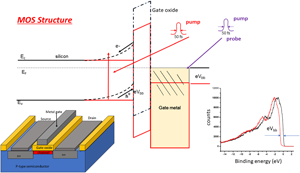
From thin film solar cells to metal–oxide–semiconductor (MOS) devices in leading edge integrated circuits, the electronic structure at and near the interfaces between component materials determines the most important fundamental operating characteristics of those devices such as turn-on voltage, power dissipation, and off-state current leakage. Fermi level location at buried interfaces, semiconductor (SC) band bending, charge transfer, oxide defects, and work functions of the constituent materials all contribute to device performance. This paper describes how these important parameters can be determined by employing femtosecond photovoltage spectroscopy, an extension of ultraviolet photoelectron spectroscopy (UPS) using ultrafast lasers. While standard UPS is fundamentally a surface-sensitive spectroscopy, pump/probe techniques add a new dimension to this venerable spectroscopy, permitting the accurate extraction of the underlying band bending in SCs. When combined with the valence band edge location of the SC and oxide, and determination of the system Fermi level, full characterization of the electronic structure of a MOS stack can be obtained providing key insights on device operating properties. This approach can be extended to study key device materials in emerging areas of artificial intelligence and quantum computing. In each case, surprising new details were uncovered that led to performance optimization of these technologically important devices.

Type
Prospective Articles
Copyright
Copyright © The Author(s), 2020, published on behalf of Materials Research Society by Cambridge University Press

Access options

Get access to the full version of this content by using one of the access options below. (Log in options will check for institutional or personal access. Content may require purchase if you do not have access.)

References

Plummer, E.W. and Eberhardt, W.: Angle-resolved photoemission as a tool for the study of surfaces. Adv. Chem. Phys. 49, 533656 (2007).CrossRefGoogle Scholar
Seah, M.P. and Dench, W.A.: Quantitative electron spectroscopy of surfaces: A standard data base for electron inelastic mean free paths in solids. Surf. Interface Anal. 1, 211 (1979).CrossRefGoogle Scholar
Krause, J.L., Schafer, K.J., and Kulander, K.C.: High-order harmonic generation from atoms and ions in the high intensity regime. Phys. Rev. Lett. 68, 35353538 (1992).CrossRefGoogle ScholarPubMed
Bartels, R.A., Paul, A., Green, H., Kapteyn, H.C., Murnane, M.M., Backus, S., Christov, I.P., Liu, Y., Attwood, D., and Jacobsen, C.: Generation of spatially coherent light at extreme ultraviolet wavelengths. Science 297, 376378 (2002).CrossRefGoogle ScholarPubMed
Backus, S., Peatross, J., Huang, C.P., Murnane, M.M., and Kapteyn, H.C.: Ti: Sapphire amplifier producing millijoule-level, 21-fs pulses at 1 kHz. Opt. Lett. 20, 20002002 (1995).CrossRefGoogle ScholarPubMed
Durfee, C.G. III, Rundquist, A.R., Backus, S., Herne, C., Murnane, M.M., and Kapteyn, H.C.: Phase matching of high-order harmonics in hollow waveguides. Phys. Rev. Lett. 83, 2187 (1999).CrossRefGoogle Scholar
Popmintchev, T., Chen, M.-C., Arpin, P., Murnane, M.M., and Kapteyn, H.C.: The attosecond nonlinear optics of bright coherent X-ray generation. Nat. Photon. 4, 822832 (2010).CrossRefGoogle Scholar
Haight, R. and Peale, D.R.: Antibonding state on the Ge (111): As surface: Spectroscopy and dynamics. Phys. Rev. Lett. 70, 3979 (1993).CrossRefGoogle ScholarPubMed
Haight, R.: Electron dynamics at surfaces. Surf. Sci. Rep. 21, 275325 (1995).CrossRefGoogle Scholar
Gauthier, A., Sobota, J.A., Gauthier, N., Xu, K.J., Pfau, H., Rotundu, C., Shen, Z.X., and Kirchmann, P.S.: Tuning time and energy resolution in time-resolved photoemission spectroscopy. arXiv Prepr arXiv200607758 (2020).CrossRefGoogle Scholar
van de Burgt, Y., Lubberman, E., Fuller, E.J., Keene, S.T., Faria, G.C., Agarwal, S., Marinella, M.J., Talin, A.A., and Salleo, A.: A non-volatile organic electrochemical device as a low-voltage artificial synapse for neuromorphic computing. Nat. Mater. 16, 414 (2017).CrossRefGoogle ScholarPubMed
Gloeckler, M. and Sites, J.R.: Efficiency limitations for wide-band-gap chalcopyrite solar cells. Thin Solid Films 480–481, 241245 (2005).CrossRefGoogle Scholar
Noufi, R. and Zweibel, K.: High-efficiency CdTe and CIGS thin-film solar cells: Highlights and challenges. In 2006 IEEE 4th World Conference on Photovoltaic Energy Conference, Waikoloa, HI, 2006; pp. 317–320. doi: 10.1109/WCPEC.2006.279455.CrossRefGoogle Scholar
Dhanam, M., Prabhu, R.R., and Manoj, P.K.: Investigations on chemical bath deposited cadmium selenide thin films. Mater. Chem. Phys. 107, 289296 (2008).CrossRefGoogle Scholar
Tauchi, Y., Kim, K., Park, H., and Shafarman, W.: Characterization of (AgCu)(InGa)Se2absorber layer fabricated by a selenization process from metal precursor. IEEE J. Photovolt. 3, 467471 (2013).CrossRefGoogle Scholar
Mansfield, L.M., Noufi, R., Muzzillo, C.P., Dehart, C., Bowers, K., To, B., Pankow, J.W., Reedy, R.C., and Ramanathan, K.: Enhanced performance in Cu(In,Ga)Se2 solar cells fabricated by the two-step selenization process with a potassium fluoride postdeposition treatment. IEEE J. Photovolt. 4, 16501654 (2014).CrossRefGoogle Scholar
Platzer-Björkman, C., Törndahl, T., Abou-Ras, D., Malmström, J., Kessler, J., and Stolt, L.: Zn(O,S) buffer layers by atomic layer deposition in Cu(In,Ga)Se2 based thin film solar cells: Band alignment and sulfur gradient. J. Appl. Phys. 100, 044506 (2006).CrossRefGoogle Scholar
Wang, W., Winkler, M.T., Gunawan, O., Gokmen, T., Todorov, T.K., Zhu, Y., and Mitzi, Y.Z.: Device characteristics of CZTSSe thin-film solar cells with 12.6% efficiency. Adv. Energy Mater. 4, 15 (2014).CrossRefGoogle Scholar
Haight, R., Barkhouse, A., Gunawan, O., Shin, B., Copel, M., Hopstaken, M., and Mitzi, D.B.: Band alignment at the Cu2ZnSn(SxSe1–x)4/CdS interface. Appl. Phys. Lett. 98, 253502-1–3 (2011).CrossRefGoogle Scholar
Ki, W. and Hillhouse, W.H.: Earth-abundant element photovoltaics directly from soluble precursors with high yield using a non-toxic solvent. Adv. Energy Mater. 15, 732735 (2011).CrossRefGoogle Scholar
Paik, H., Schuster, D.I., Bishop, L.S., Kirchmair, G., Catelani, G., Sears, A.P., Johnson, B.R., Reagor, M.J., Frunzio, L., Glazman, L.I., and Girvin, S.M.: Observation of high coherence in Josephson junction qubits measured in a three-dimensional circuit QED architecture. Phys. Rev. Lett. 107, 240501 (2011).CrossRefGoogle Scholar
McDermott, R.: Materials origins of decoherence in superconducting qubits. IEEE Trans. Appl. Supercond. 19, 2 (2009).CrossRefGoogle Scholar
Lim, D., Haight, R., Copel, M., and Cartier, E.: Oxygen defects and Fermi level location in metal-hafnium oxide-silicon structures. Appl. Phys. Lett. 87, 72902 (2005).CrossRefGoogle Scholar
del Alamo, J.A.: Nanometre-scale electronics with III–V compound semiconductors. Nature 479, 317 (2011).CrossRefGoogle ScholarPubMed
Gibson, E.A., Paul, A., Wagner, N., Gaudiosi, D., Backus, S., Christov, I.P., Aquila, A., Gullikson, E.M., Attwood, D.T., Murnane, M.M., and Kapteyn, H.C.: Coherent soft X-ray generation in the water window with Quasi-phase matching. Science 302, 95 (2003).CrossRefGoogle ScholarPubMed
Lewenstein, M., Balcou, P., Ivanov, M.Y., L'huillier, A., and Corkum, P.B.: Theory of high-harmonic generation by low-frequency laser fields. Phys. Rev. A 49, 2117 (1994).CrossRefGoogle ScholarPubMed
Haight, R. and Carr, A.V.: Industrial Applications of Ultrafast Lasers. 1st ed. (World Scientific Press, London, Singapore, 2018). ISBN 2335-6596 v. 11.CrossRefGoogle Scholar
Lim, D. and Haight, R.: In situ photovoltage measurements using femtosecond pump-probe photoelectron spectroscopy and its application to metal–HfO2–Si structures. J. Vac. Sci. Technol. A 23, 16981705 (2005).CrossRefGoogle Scholar
Carstens, H., Högner, M., Saule, T., Holzberger, S., Lilienfein, N., Guggenmos, A., Jocher, C., Eidam, T., Esser, D., Tosa, V., Pervak, V., Limpert, J., Tünnermann, A., Kleineberg, U., Krausz, F., and Pupeza, I.: High-harmonic generation at 250 MHz with photon energies exceeding 100 eV. Optica 3, 366 (2016).CrossRefGoogle Scholar
Sze, S.M. and Ng, K.K.: Physics of Semiconductor Devices (John Wiley & Sons, New Jersey, US, 2006).CrossRefGoogle Scholar
Kraut, E.A., Grant, R.W., Waldrop, J.R., and Kowalczyk, S.P.: Precise determination of the valence-band edge in x-ray photoemission spectra: Application to measurement of semiconductor interface potentials. Phys. Rev. Lett. 44, 1620 (1980).CrossRefGoogle Scholar
Chambers, S.A., Droubay, T., Kaspar, T.C., and Gutowski, M.: Experimental determination of valence band maxima for SrTiO3, TiO2, and SrO and the associated valence band offsets with Si (001). J. Vac. Sci. Technol. B 22, 22052215 (2004).CrossRefGoogle Scholar
Lim, D. and Haight, R.: Temperature dependent defect formation and charging in hafnium oxides and silicates. J. Vac. Sci. Technol. B 23, 201205 (2005).CrossRefGoogle Scholar
Dicks, O.A., Cottom, J., Shluger, A.L., and Afanasiev, V: The origin of negative charging in amorphous Al2O3 films: The role of native defects. Nanotechnology 30, 205201 (2019).CrossRefGoogle ScholarPubMed
Frank, D.J., Nowak, E., and Solomon, P.M.: Device scaling limits of Si MOSFETs and their application dependencies. Proc. IEEE 89, 259 (2001).CrossRefGoogle Scholar
Haight, R., Barkhouse, A., Gunawan, O., Shin, B., Copel, M., Hopstaken, M., and Mitzi, D.B.: Band alignment at the Cu2ZnSn (SxSe1−x)4/CdS interface. Appl. Phys. Lett. 98, 253502 (2011).CrossRefGoogle Scholar
Haight, R., Gershon, T., Gunawan, O., Antunez, P., Bishop, D., Lee, Y.S., Gokman, T., Sardashti, K., Chagarov, E., and Kummel, A.: Industrial perspectives on earth abundant, multinary thin film photovoltaics. Semicond. Sci. Technol. 32, 033004 (2017).CrossRefGoogle Scholar
Minemoto, T., Hashimoto, Y., Satoh, T., Negami, T., Takakura, H., and Hamakawa, Y.: Cu(In,Ga)Se[sub 2] solar cells with controlled conduction band offset of window/Cu(In,Ga)Se2 layers. J. Appl. Phys. 89, 8327 (2001).CrossRefGoogle Scholar
Barkhouse, D.A.R., Haight, R., Sakai, N., Hiroi, H., Sugimoto, H., and Mitzi, D.B.: Cd-free buffer layer materials on Cu2ZnSn(SxSe1-x)4: Band alignments with ZnO, ZnS, and In2S3. Appl. Phys. Lett. 100, 49 (2012).CrossRefGoogle Scholar
Haight, R., Barkhouse, A., Wang, W., Luo, Y., Shao, X., Mitzi, D.B., Homare, H., and Sugimoto, S.: CdS and Cd-free buffer layers on solution phase grown Cu2 ZnSn (SxSe1–x)4: Band alignments and electronic structure determined with femtosecond ultraviolet photoelectron spectroscopy. In MRS Proceedings, Vol. 1638 (Cambridge University Press, Cambridge, UK, 2014) p. mrsf13-1638.Google Scholar
Li, J., Wei, M., Du, Q., Liu, W., Jiang, G., and Zhu, C.: The band alignment at CdS/Cu2ZnSnSe4 heterojunction interface. Surf. Interface Anal. 45, 682684 (2013).CrossRefGoogle Scholar
Bär, M., Schubert, B.A., Marsen, B., Wilks, R.G., Pookpanratana, S., Blum, M., Krause, S., Unold, T., Yang, W., Weinhardt, L., and Heske, C.: Cliff-like conduction band offset and KCN-induced recombination barrier enhancement at the CdS/Cu2ZnSnS4 thin-film solar cell heterojunction. Appl. Phys. Lett. 99, 222105 (2011).CrossRefGoogle Scholar
Barinov, A., Dudin, P., Gregoratti, L., Locatelli, A., Menteş, T.O., Nino, M.A., and Kiskinova, M.: Synchrotron-based photoelectron microscopy. Nucl. Instrum. Methods Phys. Res. A 601, 1952002 (2009).CrossRefGoogle Scholar