Hostname: page-component-848d4c4894-75dct Total loading time: 0 Render date: 2024-05-05T20:53:22.124Z Has data issue: false hasContentIssue false

Boron doping of ultrananocrystalline diamond films by thermal diffusion process

Published online by Cambridge University Press:  13 August 2018

Pablo Tirado
Affiliation:
Departamento de Investigación en Física, Universidad de Sonora, Rosales y Luis Encinas, Hermosillo, Sonora 83000, México Department of Materials Science and Engineering, University of Texas at Dallas, Richardson, TX 75080, USA
Jesus J. Alcantar-Peña
Affiliation:
Department of Materials Science and Engineering, University of Texas at Dallas, Richardson, TX 75080, USA
Elida de Obaldia
Affiliation:
Department of Materials Science and Engineering, University of Texas at Dallas, Richardson, TX 75080, USA Facultad de Ciencia y Tecnología, Universidad Tecnológica de Panamá, Panamá, República de Panamá
Yuriy Kudriavtsev
Affiliation:
Departamento de Ingeniería Eléctrica, CINVESTAV-IPN, Ciudad de México, México
Rafael García
Affiliation:
Departamento de Investigación en Física, Universidad de Sonora, Rosales y Luis Encinas, Hermosillo, Sonora 83000, México
Orlando Auciello*
Affiliation:
Department of Materials Science and Engineering, University of Texas at Dallas, Richardson, TX 75080, USA Department of Bioengineering, University of Texas at Dallas, Richardson, TX 75080, USA
*
Address all correspondence to Orlando Auciello at orlando.auciello@utdallas.edu
Get access

Abstract

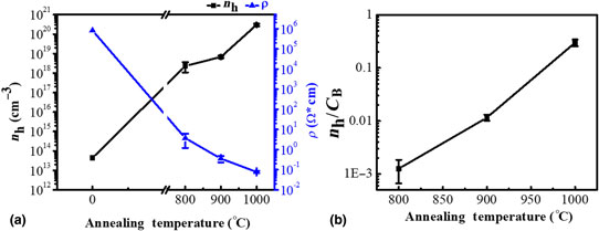
A novel process for Boron doping of ultrananocrystalline diamond (UNCD) films, using thermal diffusion, is described. Hall measurements show an increase in carrier concentration from 1013 to 1020 cm−3. Ultraviolet Photoelectron Spectroscopy and x-ray Photoelectron Spectroscopy show a band gap of 4.4 eV, a work function of 5.1 eV and a Fermi level at 2.0 eV above the valence band. Boron atoms distribution through UNCD films, was measured by Secondary Ion Mass Spectrometry, revealing Boron atoms diffusivity of about 10−14 cm2/s. Raman spectroscopy and x-ray Diffraction analysis revealed that UNCD films did not suffer graphitization nor structural damage during annealing.

Type
Research Letters
Copyright
Copyright © Materials Research Society 2018 

Access options

Get access to the full version of this content by using one of the access options below. (Log in options will check for institutional or personal access. Content may require purchase if you do not have access.)

References

1.Auciello, O. and Sumant, A.V.: Status review of the science and technology of ultrananocrystalline diamond (UNCD™) films and application to multifunctional devices. Diamond Relat. Mater. 19, 699 (2010); (www.thindiamond.com).Google Scholar
2.Fabisiak, K. and Staryga, E.: CVD diamond: from growth to application. J. Achievements Mater. Manuf. Eng. 37, 264 (2009).Google Scholar
3.Kraft, A.: Doped diamond: a compact review on a new, versatile electrode material. Int. J. Electrochem. Sci. 2, 355 (2007).Google Scholar
4.Suman, A.V., Krauss, A.R., Gruen, D.M., Auciello, O., Erdemir, A., Wlliams, M., Artiles, A.F., and Adams, W.: Ultrananocrystalline diamond film as a wear-resistant and protective coating for mechanical seal applications. Tribol. Trans. 48, 24 (2005); (www.thindiamond.com).Google Scholar
5.Zeng, H., Konicek, A.R., Moldovan, N., Mangolini, F., Jacobs, T., Wylie, I., Arumugam, P.U., Siddiqui, S., Carpick, R.W., and Carlisle, J.A.: Boron-doped ultrananocrystalline diamond synthesized with an H-rich/Ar-lean gas system. Carbon. N. Y. 84, 103 (2015).Google Scholar
6.Xiao, X., Wang, J., Carlisle, J.A., Mech, B., Greenberg, R., Freda, R., Humayun, M.S., Weiland, J., and Auciello, O.: In Vitro and In Vivo evaluation of ultrananocrystalline diamond for coating of implantable retinal microchips. J. Biomed. Mater. 77B, 273 (2006).Google Scholar
7.Suzuki, M., Ono, T., Sakuma, N., and Sakai, T.: Low-temperature thermionic emission from nitrogen-doped nanocrystalline diamond films on n-type Si grown by MPCVD. Diamond Relat. Mater. 18, 1274 (2009).Google Scholar
8.Bhattacharyya, S., Auciello, O., Birrell, J., Carlisle, J.A., Curtiss, L.A., Goyette, A.N., Gruen, D.M., Krauss, A.R., Schlueter, J., Sumant, A.V., and Zapol, P.: Synthesis and characterization of highly-conducting nitrogen-doped ultrananocrystalline diamond films. Appl. Phys. Lett. 79, 1441 (2001).Google Scholar
9.Bhattacharyya, S.: Mechanism of high n-type conduction in nitrogen-doped nanocrystalline diamond. Phys. Rev. B70, 125412 (2004).Google Scholar
10.Williams, O.: Growth and properties of nanocrystalline diamond films. Physica Status Solidi: Appl. Mater. Sci. 203, 3375 (2006).Google Scholar
11.Sun, Q., Wang, J., Weng, J., and Liu, F.: Surface structure and electric properties of nitrogen incorporated NCD films. Vacuum 137, 155 (2017).Google Scholar
12.Kato, H., Takeuchi, D., Ogura, M., Yamada, T., Kataoka, M., Kimura, Y., Sobue, S., Nebel, C.E., Yamasaki, S., Meir, S., Stephanos, C., Geballe, T.H., Mannhart, J., Suzuki, M., Ono, T., Sakuma, N., Sakai, T., Schwede, J.W., Bargatin, I., Riley, D.C., Hardin, B.E., Rosenthal, S.J., Sun, Y., Schmitt, F., Pianetta, P., Howe, R.T., Shen, Z.X., Melosh, N.A., Sun, T., and Grilj, M.: Thermionic emission characterization of boron-doped microcrystalline diamond films at elevated temperatures. Diamond Relat. Mater. 5, 165 (2013).Google Scholar
13.Seo, J., Wu, H., Mikael, S., Mi, H., Blanchard, J.P., Venkataramanan, G., Zhou, W., Gong, S., and Morgan, D.: Thermal diffusion boron doping of single-crystal natural diamond. J. Appl. Phys. 119, 205703 (2016).Google Scholar
14.Wort, C.J.H. and Balmer, R.S.: Diamond as an electronic material. Mater. Today 11, 22 (2008).Google Scholar
15.Basher, M.K. and Shorowordi, K.M.: Fabrication of monocrystalline silicon solar cell using phosphorous diffusion technique. Int. J. Sci. Res. Pub. 5, 1 (2015).Google Scholar
16.Bentzen, A., Schubert, G., Christensen, J.S., Svensson, B.G., and Holt, A.: Influence of temperature during phosphorus emitter diffusion from a spray-on source in multicrystalline silicon solar cell processing. J. Optoelectron. Adv. Mater. 15, 3 (2013).Google Scholar
17.Filik, J.: Raman spectroscopy: a simple, non-destructive way to characterize diamond and diamond-like materials. Spectrosc. Eur. 17, 10 (2005).Google Scholar
18.Birrell, J., Gerbi, J.E., Auciello, O., Gibson, J.M., Johnson, J., and Carlisle, J.A.: Interpretation of the Raman spectra of ultrananocrystalline diamond. Diamond Relat. Mater. 14, 86 (2005).Google Scholar
19.Fuentes-Fernandez, E.M.A., Alcantar-Peña, J.J., Lee, G., Boulom, A., Phan, H., Smith, B., Nguyen, T., Sahoo, S., Ruiz-Zepeda, F., Arellano-Jimenez, M.J., Gurman, P., Martinez-Perez, C.A., Yacaman, M.J., Katiyar, R.S., and Auciello, O.: Synthesis and characterization of microcrystalline diamond to ultrananocrystalline diamond films via Hot Filament Chemical Vapor Deposition for scaling to large area applications. Thin Solid Films 603, 62 (2016).Google Scholar
20.Alcantar-Peña, J.J., Lee, G., Fuentes-Fernandez, E.M.A., Gurman, P., Quevedo-Lopez, M., Sahoo, S., Katiyar, R.S., Berman, D., and Auciello, O.: Science and technology of diamond films grown on HfO2 interface layer for transformational technologies. Diamond Relat. Mater. 69, 221 (2016).Google Scholar
21.Cui, J., Ristein, J. and Ley, L.: Electron affinity of the bare and hydrogen covered single crystal diamond (111) surface. Phys. Rev. Lett. 81, 429 (1998).Google Scholar
22.Bob Downs, R.S. and Bartelmehs, K.: Interactive software for calculating and displaying x-ray or neutron powder diffractometer patterns of crystalline materials. Am. Mineral. 78, 1104 (1993).Google Scholar
23.Tyrrell, H.J.V.: The origin and present status of Fick's diffusion law. J. Chem. Educ. 41, 397 (1964).Google Scholar
24.Sung, T., Popovici, G., Prelas, M.A., and Wilson, R.G.: Boron diffusion coefficient in diamond. MRS Proc. 416, 467 (1996).Google Scholar
25.Popovici, G., Sung, T., Khasawinah, S., Prelas, M.A., and Wilson, R.G.: Forced diffusion of impurities in natural diamond and polycrystalline diamond films. J. Appl. Phys. 77, 5625 (1995).Google Scholar
26.Vickerman, J.C. and Gilmore, I.S. (eds.): Surface Analysis—The Principal Techniques, 2nd ed (John Wiley and Sons, Ltd., Hoboken, New Jersey, 2009).Google Scholar
27.Nichols, M.T., Li, W., Pei, D., Antonelli, G.A., Lin, Q., Banna, S., Nishi, Y., and Shoet, J.L.: Measurement of bandgap energies in low-k organosilicates. J. Appl. Phys. 115, 94105 (2014).Google Scholar
28.Pelaz, V.: Activation and deactivation of implanted Boron in Si. Appl. Phys. Lett. 75, 662 (1999).Google Scholar
Supplementary material: File

Tirado et al. supplementary material

Figures S1-S3

Download Tirado et al. supplementary material(File)
File 1.3 MB