


Biological Applications
Fluorescence-Based Detection of Membrane Fusion State on a Cryo-EM Grid using Correlated Cryo-Fluorescence and Cryo-Electron Microscopy by LA Metskas and JAG Briggs, Microsc Microanl | doi: 10.1017/S1431927619000606
Correlated light and electron microscopy (CLEM) has become a popular technique for combining the protein-specific labeling of fluorescence with electron microscopy, both at ambient and cryogenic temperatures. Fluorescence applications at cryo-temperature have typically been limited to localization of tagged protein oligomers due to photophysical and optical issues. Here, we present a dialkylcarbocanine DiD autoquenching-based membrane fusion assay adapted for cryo-CLEM and use it to identify areas of fusion between influenza virus-like particles and fluorescently labeled lipid vesicles. The fluorescence signal may be used either to target areas of fusion for cryo-EM imaging or to characterize the fusion state of locations chosen by cryo-EM. This result demonstrates that cryo-CLEM can be used to localize functions in addition to tagged proteins and that fluorescence autoquenching by resonance energy transfer can be incorporated successfully into cryo-CLEM approaches. In the case of membrane fusion applications, this method provides both an orthogonal confirmation of functional state, independent of the morphological description from cryo-EM, and a way to bridge room-temperature kinetic assays and the cryo-EM images.
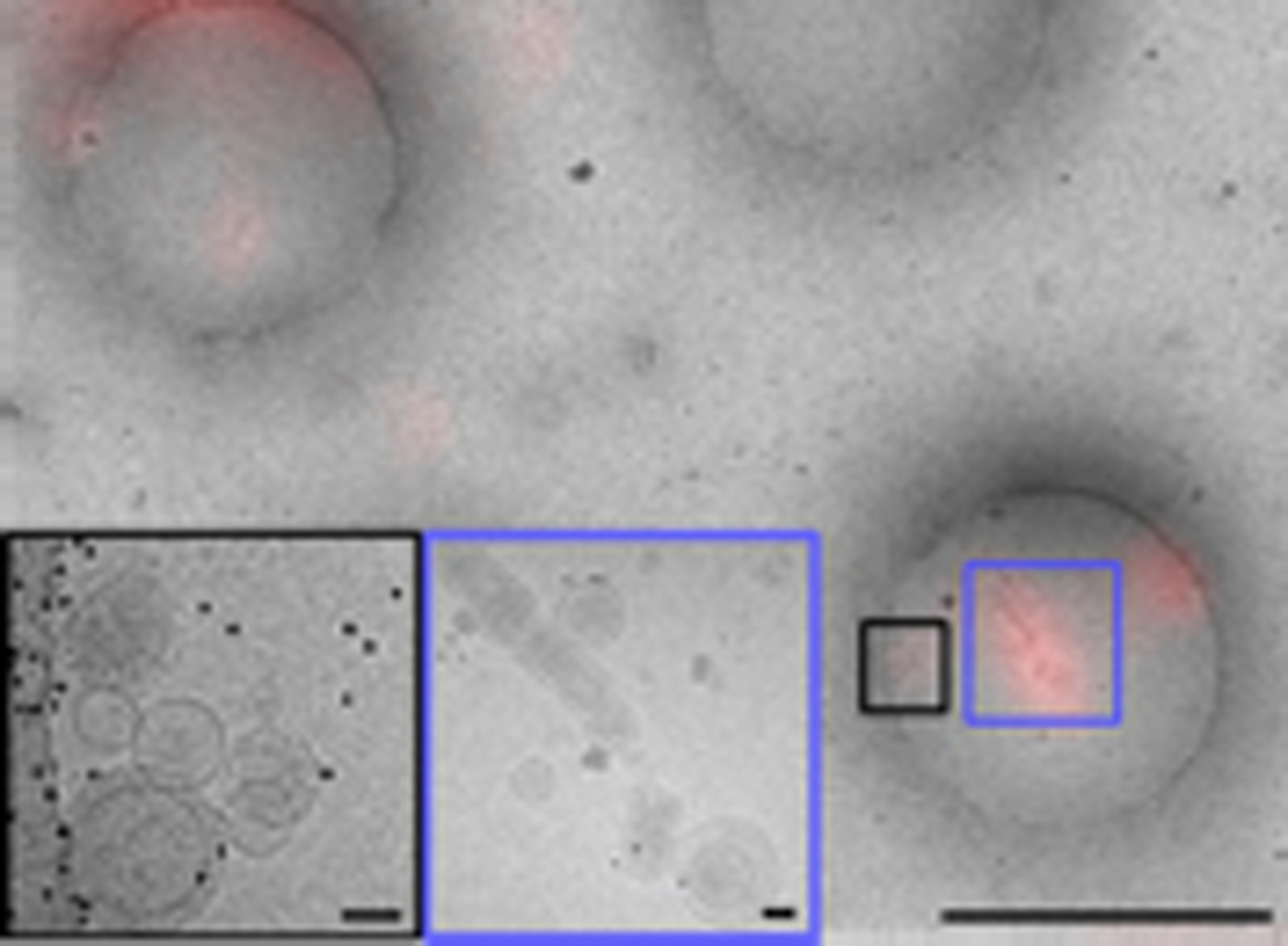
Cryo-CLEM image of influenza virus-like particles fusing with synthetic target vesicles. Strong fluorescence intensity spots (blue outline) indicate areas of lipid mixing. Inserts at left bottom: higher-resolution cryo-EM images at the indicated locations. Scale bars are 50 nanometers for inserts, 2 micrometers for larger overview.
Techniques and Material Applications
Ion Beam Induced Artifacts in Lead Based Chalcogenides by X Zhang, S Hao, G Tan, X Hu, EW Roth, MG Kanatzidis, C Wolverton, and VP Dravid, Microsc Microanal | doi: 10.1017/S1431927619000503
Metal chalcogenides have shown great potential in applications ranging from solar cells and superconductors to thermoelectrics. Microstructure, especially at the atomic and nanoscale, can alter the intrinsic properties and performance of metal chalcogenides. Scanning transmission and transmission electron microscopy (STEM and TEM) can resolve microstructure and composition at atomic scale, making them great approaches for studying the structure-property-performance relationship in metal chalcogenides. However, damage and artifacts from TEM specimen preparation can obfuscate the interpretation of intrinsic structure. We compare the effects of several TEM specimen preparation methods on the microstructure of stoichiometric lead telluride (PbTe). We observed that argon (Ar) ion milling can lead to surface irradiation damage, generating likely Pb vacancy clusters and self-interstitial atom (SIA) clusters. The SIA clusters appear as orthogonal nanoscale features along <001> orientations, reminiscent of classical nanoscale precipitates. Methods for surface damage reduction are also covered in this work, which reveal the materials’ intrinsic structure. This collective approach may assist standard protocols for future TEM specimen preparation of lead-based chalcogenides.
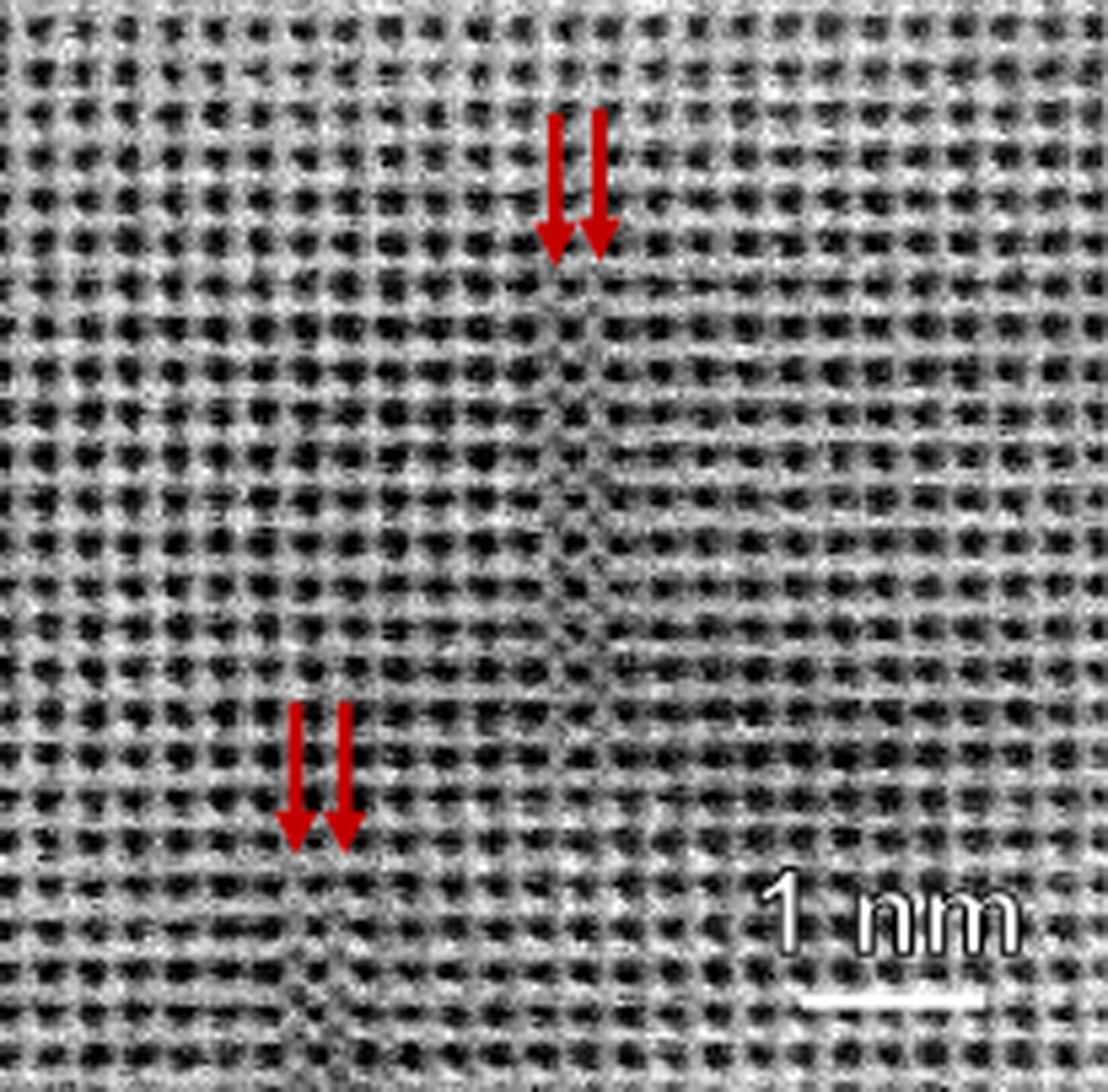
Bright-field scanning transmission electron microscopy image of ingot PbTe specimen prepared by ion milling. The ion beam induced SIA clusters are highlighted by the red arrows.
Techniques and Material Characterization
Automated Reconstruction of Spherical Kikuchi Maps by C Zhu, K Kaufmann, and KS Vecchio, Microsc Microanal | doi: 10.1017/S1431927619000710
Electron backscatter diffraction (EBSD) is a surface characterization technique, based on scanning electron microscopy, used to extract location-specific crystallographic orientation information from crystalline materials. The conventional EBSD setup allows real-time orientation determination from two-dimensional Kikuchi patterns. Those Kikuchi patterns are gnomonically projected onto a flat phosphor screen, although the electron diffraction that originates from the point source produces a three-dimensional spherical Kikuchi map with specific orientations dictated by the orientation of the crystal. We report in this study a fully automated method to recover the spherical Kikuchi map from experimental Kikuchi patterns. First, experimental patterns are filtered based on the pattern quality, relative misorientation, and the cross-correlation coefficient with simulated patterns. Next, an inverse gnomonic projection is implemented to transform the collected pattern in the gnomonic projection frame to the detector frame before rotating it into the correct orientation in the Cartesian crystal frame (Figure). This method potentially enables more accurate orientation determination, new pattern center refinement methods, and improved EBSD-based phase identification.

(Top) Crystal unit cell of aluminum; (middle) a kinematically simulated Kikuchi sphere for aluminum at 20 kV; (bottom) a reconstructed spherical Kikuchi map from experimental patterns for aluminum at 20 kV.
