


Introduction
Solid materials in subambient gaseous environments have been imaged using in situ transmission electron microscopy (TEM), for example to study dynamic effects: carbon nanotube growth [Reference Helveg, Lopez-Cartes, Sehested, Hansen, Clausen, Rostrup-Nielsen, Abild-Pedersen and Norskov1], nanoparticle changes during redox reactions [Reference Crozier, Wang and Sharma2], and phase transitions in nanoscale systems [Reference Kim, Tersoff, Wen, Reuter, Stach and Ross3]. In these studies the vacuum level in the specimen region of the electron microscope was increased to pressures of up to 10 mbar using pump-limiting apertures that separated the specimen region from the rest of the high-vacuum electron column [Reference Ruska4], but it has not been possible to achieve the higher pressures that are desirable for catalysis research [Reference Gates5]. TEM imaging at atmospheric pressure and at elevated temperature was achieved with 0.2-nm resolution by enclosing a gaseous environment several micrometers thick between ultra-thin, electron transparent silicon nitride windows [Reference Creemer, Helveg, Hoveling, Ullmann, Molenbroek, Sarro and Zandbergen6]. Although Ångström-level resolution in situ TEM has been demonstrated with aberration-corrected systems [Reference Gai and Boyes7], the key difficulty with TEM imaging is its dependence on phase contrast, which requires ultra-thin specimens, limiting the choice of experiments.
The parameter space changes radically when using scanning transmission electron microscopy (STEM). We have recently introduced a simple and inexpensive system for in situ for STEM imaging through 360 micrometers of gas at atmospheric pressure [Reference Bigelow and Veith8].
Instrumentation
In the present work, the flow cell was composed of two silicon microchips supporting silicon nitride (SiN) windows placed directly in the vacuum chamber of the electron microscope (Figure 1). A 0.36-mm spacer created a gap between the chips. Plastic tubing mounted into the flow cell allowed gas to flow to and from the sample. The entire flow cell and the tubing were sealed with epoxy. Nanoparticles were fixed on the entrance window, which was defined with respect to the electron beam direction. Images were obtained by scanning the focused electron beam over the sample and detecting elastically scattered electrons with an annular dark-field (ADF) detector.
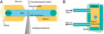
Figure 1: Schematic of the flow system for atmospheric-pressure STEM. (A) A cross section of a sample compartment filled with gas at atmospheric pressure is enclosed between two silicon microchips supporting electron-transparent SiN windows. The microchips are separated by a spacer and sealed with epoxy. The flow cell is placed in the vacuum of the electron microscope. Images are obtained by scanning a focused electron beam over nanoparticles attached to the top window and detecting elastically scattered transmitted electrons. The dimensions and angles are not to scale. (B) Top view schematic of the flow cell. The gas flow path is from the input tubing, over the SiN window in the interior of the flow cell, and out the output tubing. Small pieces of tubing serve as the spacer. Figure modified from [Reference Bigelow and Veith8].
The dimensions of the silicon microchips (Protochips, Inc.) were 2.00 × 2.60 × 0.30 mm3, and each chip supported a 50 μm × 200 μm × 50 nm SiN window [Reference Peckys, Kremers and Piston9] (Figures 2A and 2B). These dimensions presented an optimum balance between the field of view and the strength to withstand the pressure difference between the interior of the flow cell and the vacuum of the electron microscope. The sides of the silicon chips were diced vertically with a precision of ±10 μm with respect to the SiN window to aid in the precise alignment of the two microchips.
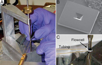
Figure 2: Assembly of the flow cell. (A) Picture of the microchips being glued together with epoxy. The chips are kept in position by a loading device with two poles. (B) SEM image showing the backside of a microchip; the opening for the silicon nitride window is visible in the middle. (C) Picture of the assembled flow cell kept in place between the metal poles of the loading device. The plastic tubing is glued in place using epoxy.
A thin-film Au/TiO2 catalyst sample was prepared on the SiN side of one of the Si chips before it was assembled into a flow cell [Reference Bigelow and Veith8]. Gold supported on TiO2 was selected as the catalyst because of the high contrast of gold in the STEM, the room temperature activity of Au/TiO2 toward the oxidation of CO, and the exothermic nature of CO oxidation. This reaction provides heat, which promotes gold migration that could be studied in the electron microscope [Reference Veith, Lupini, Rashkeev, Pennycook, Mullins, Schwartz, Bridges and Dudney10]. We used a catalyst with lower activity compared to other Au/TiO2 catalysts [Reference Veith, Lupini, Rashkeev, Pennycook, Mullins, Schwartz, Bridges and Dudney10], thus avoiding gold particle migration and coarsening for the purpose of testing the flow cell.
The flow cell was assembled using a locally designed mounting device. The device consisted of two thin poles to support the chips from the bottom and to hold them in place from the top. There was also a movable arm to aid in balancing the chips on the bottom pole; this arm can be moved away from the chips for the final assembly steps.
The silicon chip with the catalyst sample was placed with the SiN side facing up on the bottom pole of the mounting device. Using tweezers, short (<2 mm) pieces of plastic tubing (Peek tubing, Upchurch Scientific) with an inner diameter of 50 μ and an outer diameter of 0.36 mm were placed on the chip to serve as spacers. The second chip was then placed with the SiN side facing down on top of this stack, and the top pole of the mounting tool was lowered. The chips were precisely aligned by lightly squeezing the diced edges of the chips with tweezers. The chips were then sealed with vacuum epoxy (Torr Seal, Varian), leaving one of the long sides open (the left side as seen in Figures 1 and 2). After two hours of drying, the gas-flow tubing (typically ~1 m long each) was inserted into the open side of the flow cell and fixed in place with epoxy. The stack was dried overnight. The assembled flow cell and the flow cell with tubing is shown in Figures 2C and 3, respectively.
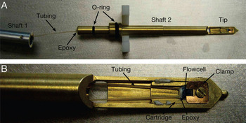
Figure 3: Specimen holder for atmospheric pressure STEM. (A) Picture of the specimen rod (Hitachi style) consisting of two shafts. Shaft 1 (left) leads the tubing to the exterior of the microscope. Shaft 2 contains the tip positioned in the center of the microscope. The flow cell is placed in the tip, and its tubing is fed through the hollow interior of shaft 2 and epoxied in place at the end of the shaft. Shaft 2 fits into shaft 1, sealed by the small O-ring. The larger O-ring provides a vacuum seal in the microscope. (B) Close-up of the tip. The flow cell is fixed in place inside a cartridge with a clamp. Pictures from [Reference Bigelow and Veith8].
The flow cell, with tubing attached to it, was then placed in a locally designed specimen rod (Figure 3). The rod consisted of two separable shafts, where shaft 2 fit into shaft 1. The smaller O-ring in Figure 3A provided the vacuum seal between the shafts, and the tubing fit through their hollow interior. A vacuum seal was made with epoxy at the outer end of shaft 1 (left side of Figure 3A), which sealed the tubing in place. The flow cell was then placed into a cartridge, which was placed into the tip of the rod and held in place by a spring clamp and screw (Figure 3B). The purpose of the cartridge was to provide the ability to reshape the tip region if needed, without having to change the whole shaft. The contents of the rod were separated from the vacuum of the microscope by the larger O-ring shown in Figure 3A.
Methods
Electron microscopy was performed in high-resolution mode with a Hitachi HD-2000 STEM at 200 kV using a probe current of approximately 0.1 nA. First, the vertical position of the stage was adjusted by focusing on the top window of the flow cell using the secondary electron detector. The flow cell was then imaged in transmission mode with the ADF detector. The brightness and contrast settings were adjusted for optimal visibility of the gold nanoparticles. Images of 1280 × 960 pixels were recorded with a 10-second acquisition time. Images were first recorded with the tubing open, thus with the interior of the flow cell at atmospheric pressure. This experiment verified that the windows did not rupture at atmospheric pressure when exposed to the electron beam. The tubing was then connected using valves and fittings (Upchurch Scientific) to a premade mixture of 1-percent CO, 5-percent O2, He (Air Products) stored in an Al cylinder to prevent the formation of Fe(CO)5. Gas entered the cell at slightly higher than ambient barometric pressure (743 torr, for the location of the experiment). Gas flow was verified by observing the volume of water displaced in an inverted graduated cylinder containing water, and flow rates were estimated to be about 0.4 cc/hour (>200 gas exchanges/hour). The integrity of the flow cell was confirmed because we maintained vacuum in the electron microscope in this configuration.
Results
Figure 4A shows a STEM image of gold nanoparticles adjacent to a 0.36-mm thick layer of CO/O2/He gas mixture at atmospheric pressure. Image noise was reduced using a convolution filter with a kernel of (1, 1, 1; 1, 5, 1; 1, 1, 1) (Image J software, NIH). The image shows several different sizes of gold islets. The background signal varied over the image, which possibly can be explained by a combination of thickness variation in the TiO2 layer and the formation of carbon contamination during imaging. Two of the smallest nanoparticles are indicated with the arrows 1 and 2. Line scans over these nanoparticles are shown in Figures 4B and 4C. They exhibit a FWHM of the peak above the background level of 0.8 nm and 1.0 nm, respectively. The spatial resolution was 0.4 nm [Reference Bigelow and Veith8].
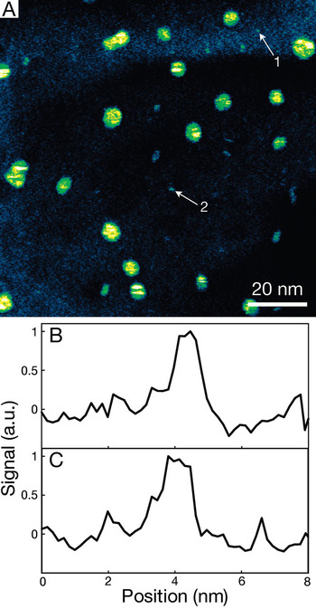
Figure 4: Atmospheric STEM image of gold nanoparticles in a 360-m thick 1-percent CO/ 5-percent O2/ He gas-filled enclosure. (A) Image showing gold islets on the top SiN window recorded at a magnification M = 600,000, a pixel size of 0.17 nm, a pixel-dwell time of 8 seconds. For improved visibility of the nanoparticles, a convolution filter was applied and the signal intensity was color-coded. (B) Line scan, signal versus horizontal position, over the nanoparticle indicated with arrow 1 in (A). The background level was set to zero. (C) Line scan, signal versus horizontal position, over the nanoparticle indicated with arrow 2 in (A). From [Reference Bigelow and Veith8].
Discussion
The electron probe of the STEM enters the flow cell through the top SiN window. The interaction between the window and the electron beam leads to a small amount of broadening of the electron probe only [Reference Bigelow and Veith8]. The beam is elastically scattered by the specimen located immediately below the SiN window, and this forms the contrast for the ADF detector. The scattered electrons then interact with the gas molecules of the 0.36-mm thick layer of 1-percent CO, 5-percent O2, He at atmospheric pressure. The effect of these interactions can be calculated from the elastic scattering cross section and mean free path length [Reference Reimer11]. The mean free path length in, for example, He2 gas at atmospheric pressure is 4 mm [Reference Bigelow and Veith8]. Because the mean free path length is much larger than the thickness of the gas column, the efficiency of detection will not change noticeably from that of imaging in a vacuum. Inelastic scattering can be neglected because it does not affect the angles of the electrons scattered into the ADF detector but merely causes a small reduction in the energy of some of the electrons compared to the total beam energy. Higher pressures than ambient pressure can probably be achieved with the present system, and, if needed, smaller or thicker SiN windows could be used. Atomic resolution should be achievable when using aberration-corrected STEM. Advanced microchip technology can be used to provide heating and cooling rates of 106 degrees Celsius per second [Reference Allard, Bigelow, Jose-Yacaman, Nackashi, Damiano and Mick12].
Conclusions
Our results show that subnanometer resolution can be achieved through a 0.36-mm thick layer of gas at atmospheric pressure, using a simple and inexpensive system that is compatible with current electron microscopes. The relatively large space between the SiN windows, and the ability to control the pressure of the sample, opens the possibility for a wide variety of experiments, involving clusters of nanoparticles, micrometer-sized samples, electrodes, mechanical probes, actuators, sensors, and even light guides, all without the need for complex, expensive equipment.
Acknowledgements
We thank L.F. Allard, P.S. Herrell, and D.C. Joy for help and discussions. The silicon chips were designed in collaboration with Protochips Inc. (NC). This research was conducted at the Center for Nanophase Materials Sciences, which is sponsored at Oak Ridge National Laboratory by the Division of Scientific User Facilities, U.S. Department of Energy. Financial support by the Laboratory Directed Research and Development Program of Oak Ridge National Laboratory, managed by UT-Battelle, LLC, for the U.S. Department of Energy (GMV, NJ), and by Vanderbilt University Medical Center (EAR, NJ).


