


Events Prior to 1967
The history of the atom probe is a shared history with electron microscopy and the quest to image atoms. It begins with a classic experiment that provided an initial verification for the quantum theory of matter. In 1928 Eyring, Mackeown, and Millikan (later of oil drop fame) published “Field Currents from Points” in which they measured a current from a sharply pointed metal cathode in an evacuated glass bulb (Figure 1), which was not predicted by the classical physics known at the time [Reference Eyring1]. Eyring, Mackeown, and Millikan further showed that “... an attempt was made to draw a current when the point was made the anode. No current was obtained when 100,000 volts was applied from a direct current generator built in this laboratory. This corresponds to a field at the point of 35 × 108 volts per centimeter.” Little did they know that they were at an order of magnitude greater electric field than needed to field evaporate iron atoms from the tip. The exponential dependence of the current on the voltage that they measured was explained theoretically in 1928 by Fowler and Nordheim by evoking the purely quantum mechanical process known as “tunneling” [Reference Fowler and Nordheim2].
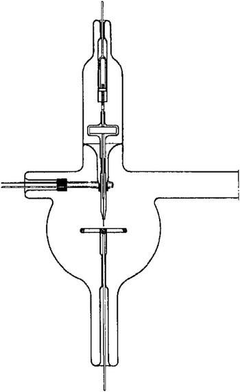
Figure 1 Apparatus used in the 1928 field emission experiments by Eyring et al. [Reference Eyring1]. A steel needle and anode were used.
In 1937, a year after Johnson and Shockley published electron emission images from a cylindrical geometry [Reference Johnson and Shockley3], Erwin Wilhelm Mìller placed a finely powdered mineral (Willemite, that fluoresces under electron bombardment) on the cathode of an apparatus and the field emission microscope, or FEM as we know it, was born [Reference Mìller4]. The electron image in the FEM reflects the variation in work function on the apex of the cathode point at a magnification of 106 and a resolution of about 10 nm. The magnification can be varied by changing the distance between the cathode and the anode, and the image is insensitive to external vibrations. The FEM demonstrated that the work function of a metal surface depends on its crystallography. It therefore explained the puzzling variation in photoelectron emission measured from flat cathode surfaces since Millikan’s 1914 experiment that confirmed Einstein’s explanation of the photoelectric effect in 1905. The FEM was also a boon to the emerging vacuum tube industry because Mìller showed that the addition of a low-work-function material like barium could be evaporated onto a cathode tip to decrease its work function, thereby greatly increasing its thermionic emission of electrons. It was possible to see structure in the emission pattern that was consistent with the crystallographic symmetry present in the specimen [Reference Mìller5]. Over the next decade, with steady improvement in quality and resolution of the patterns, there was great interest to see if the technique could be improved all the way to resolving atoms. Mìller pursued this ideal into the 1940s. His work was interrupted severely by World War II. Indeed, he almost died of starvation in Germany during that time since scientists who did not cooperate with the Third Reich were ostracized.
After the war, Mìller was invited to emigrate to the USA, and he chose Pennsylvania State College (now University) because the locale reminded him of his home region. Here, his work took a turn. One of the techniques used to improve the resolution of FEM images was to clean the tip by reversing the polarity. This seemed to remove adsorbed gases and gave sharper FEM images. At some point, Mìller and his group considered whether there was any structure in the projection of the desorbed gasses, much like FEM images. They introduced a gas into the vacuum to ensure a supply of gas atoms on the needle (Figure 2a) and indeed found detailed structure in the projected pattern. Since the electric field was oriented now to remove positive charge from the specimen, they knew that these gas atoms must be positively ionized. They thought these ions were desorbing from the surface. By 1951, they published their first field ion micrographs (FIM) [Reference Mìller6]. These FIM images (see Figure 2b) showed greater detail than the FEM images almost from the start. The obvious exciting question was whether the technique could be improved to resolve atoms. There were false starts and some luck, but eventually, on October 10, 1955, Mìller and his graduate student, Kanwar Bahadur, recorded the first ever images of atoms [Reference Bahadur7–Reference Mìller and Bahadur8] (Figure 2c). Melmed has provided a summary of the events leading up to this momentous occasion [Reference Melmed9]. You might think that the first humans ever to image atoms would have received the highest possible accolades. Unfortunately, it did not happen. It is thought by many in the field that Ruska and Mìller were being considered to share a Nobel Prize in Physics in the late 1970s but Mìller died unexpectedly in May 1977. Ruska later shared the prize in 1986 with Binnig and Rohrer of scanning tunneling microscope fame.
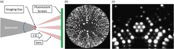
Figure 2 Field ion microscopy (FIM). (a) Schematic of an FIM instrument where the gas supply is usually an inert gas at about 10-3 Pa. (b) The first FIM images showed ledges of a tip surface [Reference Mìller6]. (c) First ever images to show individual atoms were recorded on October 11, 1955, by Bahadur and Mìller [Reference Bahadur7, Reference Mìller and Bahadur8] as recounted by Melmed [Reference Melmed9].
The Atom Probe is Born
Field ion microscopy was a big success, and it led to some publicity for Mìller and his group. For the next decade, FIM was used by a growing community of scientists to image such things as defects in materials: vacancies, interstitials, dislocations, cavities, and grain boundaries [Reference Miller10–Reference Miller11]. After a decade of atomic-scale imaging, one can imagine that the practitioners of FIM had to be wondering if they could do more than just image atoms on the surface: could they also identify them? In FIM, one can observe a static field ion image and see it change as specimen atoms evaporate in the high electric field. Mìller’s group again took the initiative and sought to apply mass spectroscopy techniques to field-evaporated atoms. Doug Barofsky, a graduate student in the group, was tasked with adapting a magnetic sector mass spectrometer to the field evaporated atoms (as recounted in [Reference Panitz12]). Before long Barofsky realized that time-of-flight (ToF) mass spectroscopy would likely be the more successful method. Mìller assigned another graduate student, John Panitz, to this task. Note that not only did Panitz need to sort out a ToF configuration, but he also had to figure out how to detect single atoms! This had never been done before. Within a year Panitz had built an instrument that could image a tip with FIM, position a particular atom inside an aperture on the image screen, pulse the electric field on the specimen to initiate an evaporation event, and detect that atom (as an ion) and determine its flight time (Figure 3) [Reference Mìller13]. By analogy with the electron microprobe, which had gained prominence in the 1960s, Mìller dubbed this instrument the atom probe [Reference Mìller13]. Because it utilized a field ion microscope, it was often referred to as an atom-probe field ion microscope (APFIM). Within months of their first public disclosures, other groups in the world had replicated the feat. Atom probes sprung up in Pittsburgh at US Steel under Sid Brenner, at the University of Oxford under George Smith, at Cornell University under David Seidman, and at the Technical University of Chalmers in Gothenburg under Hans Nordén.
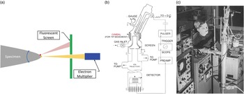
Figure 3 The atom probe field ion microscope (APFIM) [Reference Mìller13]. (a) Schematic of the probe hole geometry for APFIM. The specimen may be tilted to select that either the yellow atom or the red atom passes through the probe hole to the detector. (b) Overall schematic of the first APFIM. (c) John Panitz at the first APFIM instrument at Pennsylvania State University. Quartz tubing was used for the specimen and gimble and stainless steel for the flight tube.
Atom Probes Grow Up
The first atom probes were one-dimensional; that is, the data structure consisted of detected atoms in a sequence that represented depth into the specimen. Figure 4 shows the application of an atom probe to the study of carbon distribution in steels [Reference Williams14]. One could discern the composition of each of the phases in a material at the atomic scale as a one-dimensional composition profile. The first commercial atom probe was built in the late 1970s by Vacuum Generators in cooperation with the group at the University of Oxford under the leadership of George Smith. It was not long before the desire arose to detect not just the few ions that passed through a small aperture, but all the atoms field evaporated from the specimen. Panitz took a key step in this direction when he developed the 10 cm atom probe [Reference Panitz15] shown in Figure 5, followed later by the imaging atom probe (IAP) [Reference Panitz16]. These were the first truly three-dimensional atom probes since they could detect all of the ions of a given species (with 100% detection efficiency) by time gating for the flight time of those ions on a large detector [Reference Panitz and Foesch17]. Now, for example, all the carbon atoms in a phase could be seen over an area. The third dimension of the image is the sequence of evaporation events that coincide with depth into the specimen as in the one-dimensional atom probe. Alas, the IAP could not map all atom types at the same time. This required detector technology, yet to be invented, that could record each atom’s hit time and its position on the detector.
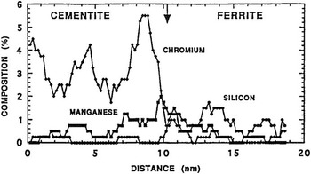
Figure 4 One-dimensional composition profile across a cementite-ferrite interface in a chromium-containing pearlitic steel. The arrow suggests the location of the interface. Reprinted with permission from [14]. Copyright 1981, TMS, Warrendale, PA.
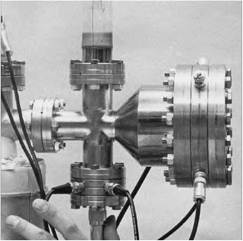
Figure 5 The 10 cm atom probe [Reference Panitz15]. This design radically changed the geometry of atom probes such that the entire emitting surface could be viewed rather than a single probe hole. It is the progenitor of today’s three-dimensional atom probes.
In the early days of atom probe, pulsing of the evaporation event was done exclusively by pulsing the electric field applied to the specimen. The specimen must have high electrical conductivity for this form of pulsing, and so all the early work in atom probe was done on metals. In the late 1970s, interest was growing to find a way to pulse non-metals, and experiments with pulsed laser heating were conducted by Kellogg and Tsong [Reference Kellogg and Tsong18]. These experiments succeeded and eventually, as recounted below, laser pulsing became the dominant mode of pulsing by 2010. All manner of materials can now be analyzed in the atom probe regardless of their electrical conductivity.
Atom Probe Tomography is Born
An attempt to overcome the limitations of the IAP was made by Michael Miller in the mid-1980s [Reference Miller19]. This instrument was never built, but it did spark interest in his ideas. The first working atom probe to map all detected atoms in three dimensions was developed in the late 1980s when Alfred Cerezo, Terry Godfrey, and George Smith adapted a position-sensitive detector to a VG APFIM 100 [Reference Cerezo20–Reference Cerezo21] and called it the position-sensitive atom probe (PoSAP). The images were awe-inspiring. Here now was an instrument that could map the atomic composition in three dimensions with atomic-scale resolution. The community dubbed these instruments three-dimensional atom probes (3DAP). The group at the Université de Rouen soon developed a 3DAP called the tomographic atom probe (TAP) [Reference Blavette22–Reference Blavette23], which generated similarly spectacular images. Eventually, the Oxford group founded a company, Kindbrisk (later called Oxford NanoScience), to commercialize the PoSAP. The Rouen group developed a relationship with CAMECA SAS in Paris to commercialize the TAP. By 1995, both companies were selling 3DAPs at the rate of about one per year. Interest in the technique grew.
Toward Higher Performance
As spectacular as the images from 3DAPs were, there were some serious challenges. Firstly, the data were generated at a rate of about 1 atom per second. A million-atom dataset, which is small for materials studies, would take over a week to collect. The largest images recorded were a couple of million ions. The mass resolving power was limited to about 200 by the fact that field pulsing was used, which introduces an energy spread on the evaporated ions. The field of view, about 15 to 20 nm diameter, was not very large. In a ToF instrument, if you move the detector toward the source, the image size increases, but the flight times decrease and the mass resolution degrades. About this time, Osamu Nishikwa presented a concept he called the scanning atom probe (SAP) [Reference Nishikawa and Kimoto24–Reference Nishikawa25]. The intent was to make it possible to analyze sharp protrusions that might occur or be fabricated on a surface by applying the high electric field from an aperture at the apex of a hollow cone. Nishikawa built an instrument where the aperture was scanned across a surface with a high potential applied, and a detector collected ions that were field evaporated from a sharp protrusion.
About this time in 1993, Tom Kelly was pursuing ways to improve the 3DAP and was struck by the potential of the conical aperture idea to effect improvements. The low data rate of 3DAPs at the time was a consequence of the technology used to perform field pulsing: reed switches were used to produce about 100 pulses per second with a detection rate of one atom per 100 pulses. Because of the proximity of the counter electrode in a SAP, the electric field was notably higher than with a remote counter electrode. This made it possible to lower the amplitude of the voltage pulse required, which made it possible to achieve several orders of magnitude greater pulse repetition rates. Because the voltage was lower, post acceleration of the ions could be used to reduce the relative energy spread of the evaporated ions. This gave a direct improvement in the mass resolution. The mass resolution improvement was independent of field of view, so the field of view could be increased. The net effect of these improvements was a 3DAP that had a data collection rate of a million atoms per minute (16,000 atoms per second) with a mass resolving power of 500 over a field of view greater than 100 nm. The largest data sets have reached a billion ions from a single specimen. The local electrode was the key to these improvements, and the instrument was called the local electrode atom probe or LEAP [Reference Kelly26–Reference Kelly and Larson27]. Figure 6 shows a schematic of the key components [Reference Giddings28].
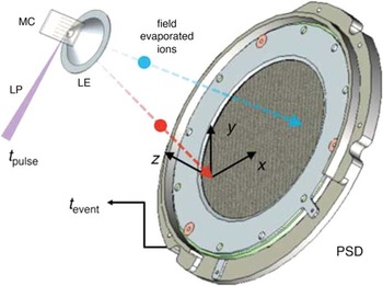
Figure 6 Schematic of a local electrode atom probe (LEAP). MC is a microtip coupon, LP is a laser pulse, LE is the local electrode, and PSD is the position-sensitive detector. Reprinted with permission from [Reference Giddings28]. Copyright 2014 Cambridge University Press.
Laser pulsing was applied to 3DAPs first by Cerezo et al. [Reference Cerezo29–Reference Cerezo30] and later by Gault et al. [Reference Gault31] and Bunton et al. [Reference Bunton32]. Laser pulsing has been a crucial component of the success of atom probe tomography (APT) in the past decade because it opened the possibility of analysis of materials with low electrical conductivity, that is, semiconductors and insulators.
A Commercial LEAP
In 1998, Tom Kelly founded Imago Scientific Instruments Corporation to commercialize the LEAP. The first instrument was purchased and shipped in 2003 to Michael Miller at Oak Ridge National Laboratory. Imago was acquired in 2010 by Ametek, Inc. and was made part of CAMECA SAS. As of 2017, over 100 LEAPs have been shipped. The field has grown markedly as evidenced by the growth in the number of publications per year, which correlates with the number of instruments shipped. There is one other commercial instrument that is being developed by a group headed by Guido Schmitz at the University of Stuttgart. This instrument is designed to be attached to a focused ion beam (FIB) instrument so that specimens may be prepared by the FIB and travel to the atom probe without being exposed to atmosphere [Reference Schmitz33].
The unique strength of APT lies in its ability to determine compositions in 3D. Figure 7 shows an atom cloud of a reconstructed dataset taken from a commercial blue light-emitting diode [Reference Giddings28]. A complex structure is apparent. Figures 8a to 8c show one-dimensional elemental compositional profiles generated from within the reconstructed volume. Four distinct regions are identified, labeled α through δ, each with different roles and alloy concentrations. It used to be that manufacturers of such devices could sleep comfortably at night knowing that it would be very difficult for competitive analysis to reveal the details of their structures. Not any more.
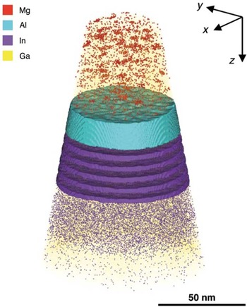
Figure 7 Atom map of a commercial light-emitting diode (LED). Single points mark the positions of detected atoms. Colors are used to represent different elements: Mg is represented by red, Al by cyan, In by indigo, and Ga by yellow. Isosurfaces indicate volumes containing concentrations greater than 3.0 at.% Al and 3.0 at.% In. Reprinted with permission from [Reference Giddings28]. Copyright 2014 Cambridge University Press.
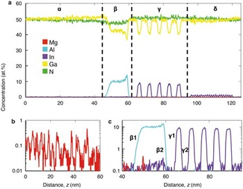
Figure 8 Time-of-flight mass spectrometry. (a) One-dimensional composition profiles of the data shown in Figure 6. Four distinct regions are evident from the profile. Region α is composed of 0.07 at.% Mg ions in addition to the GaN matrix; a close-up of this profile is shown in (b). Regions deeper into the device exhibit layers with rapid composition changes: β contains 10 at.% Al ions, and γ contains a high concentration (7.2 at.%) of In ions in a periodic structure. A close-up of this region is shown in (c), with the interfaces between the doped and undoped regions respectively labeled. δ contains a low concentration of In atoms. Reprinted with permission from [Reference Giddings28]. Copyright 2014 Cambridge University Press.
Composition analyses from grain boundaries in ceramic materials can be challenging with electron beam techniques due to radiolysis. Reliable light element analyses can be especially difficult to obtain. Ten years ago, atom probe analysis of ceramics had never been achieved and was thought by some to be impossible. Modern laser pulsing methods, however, have made it straightforward to obtain such analyses. Figure 9 shows an example from work by Diercks et al. [Reference Diercks34] on Nd-doped ceria near a grain boundary. The composition maps in the figure are for four elements that exhibit significant segregation to or away from the grain boundary, depending on the surrounding matrix. The techniques employed here are directly applicable to other technologically relevant polycrystalline ceramics and create opportunities for correlating nano-scale composition with macro-scale properties for optimizing materials design, expanding progress in ionic chemistry theory, and refining simulations for “real-world” polycrystalline materials.
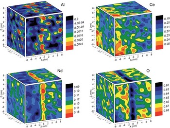
Figure 9 Concentration maps (red is high, blue/black is low) for four elements in the vicinity of a grain boundary in Nd-doped ceria. The elements have segregated in different amounts, but all show clear segregation levels toward (Al, Ce, Nd) or away (O) from the boundary. Concentrations are given in mass fractions. Reprinted with permission from [Reference Diercks34]. Copyright 2016 Royal Society of Chemistry.
Conclusion
APT has come a long way since the first atom probe in 1967. Like electron microscopy, its humble roots in mid-twentieth century have led to an essential microscopy and microanalysis tool for the twenty-first century. We can only imagine what the next 50 years will bring.


