


Introduction
Both atomic force microscopy (AFM) and Raman spectroscopy are techniques used to gather information about the surface properties of a sample. There are many reasons to combine these two technologies, and this article looks both at the complementary information gained from the techniques and how a researcher having access to a combined system can benefit from the additional information available.
Two Surface Analysis Methods
Atomic force microscopy. In AFM, a sharp probe is brought into close proximity with a sample and held at that distance by means of a force-based feedback loop [Reference Binnig, Quate and Gerber1]. In addition to the force on which the primary feedback loop is based, different quantities such as electrical current, surface potential, or specific nanomechanical properties can be measured. By scanning tip and sample relative to each other and measuring these quantities at discrete locations in a serial fashion, three-dimensional images of selected sample properties can be created. The information from AFM has proven to be extremely useful for scientific research, but it lacks the chemical specificity available from vibrational spectroscopies.
Raman spectroscopy. Spectroscopy is the study of the interaction of electromagnetic radiation with matter. The most common kinds are X-ray, fluorescence, infrared, and Raman [Reference Kuzmany2]. The latter two are vibrational techniques, that is, the energy of radiation employed is sufficient to excite molecular or lattice vibrations. In a Raman experiment the sample is illuminated with monochromatic light, and the inelastically scattered light is detected. If a sample is illuminated with light of a frequency v 0, most of the scattered light is Raleigh scattered, that is, elastically scattered without a change in frequency. A small portion, however, is scattered at a different frequency v 1 because of a change in the polarizability of the illuminated molecule. This shift is referred to as the Stokes shift if v 1 is red-shifted with regard to the incident light, or anti-Stokes if v 1 is blue-shifted. A plot of the measured intensity of these shifts versus the frequency is referred to as a Raman spectrum and is a representation of the vibrational modes excited by the Raman light source [Reference Harris and Bertolucci3].
Raman spectroscopy can provide information about a variety of materials-related phenomena: (a) composition by analyzing bands at characteristic frequencies (fingerprint), (b) symmetry or orientation of molecules or crystals by monitoring peaks using polarization techniques for the incident and scattered light [Reference Berweger, Neacsu, Mao, Zhou, Wong and Raschke4], or (c) measurement of stress or strain in a crystal by analyzing, for example, the frequency shift of a characteristic Raman band. For an in-depth review article about how Raman spectroscopy can be applied to popular sp2 carbon allotropes, see reference [Reference Saito, Hoffmann, Dresselhaus, Jorio and Dresselhaus5].
As a direct probe of the vibrational structure, Raman does not depend on the presence of an electronic state with high fluorescence quantum yield (in contrast to fluorescence), giving it wide applicability as a probe of chemistry and symmetry. This can be especially useful for the analysis of bio-related systems because Raman, unlike fluorescence, does not require labeling of the sample. What makes Raman spectroscopy challenging is that its cross section is quite small. Only 1 in a million photons interacting with a sample will be inelastically scattered and thus exhibit a Raman shift, while the other photons are simply Raleigh scattered. To get enough signal for analysis, acquisition times of several tens of seconds per location may become necessary.
A Raman spectrometer is often combined with a light microscope to take advantage of the good spatial resolution that a confocal optical setup can offer. The main components of a dispersive Raman setup are a laser to illuminate the sample, optics to collect the backscattered radiation, a laser-line rejection filter, and a spectrometer consisting of an entrance slit, a diffraction grating, and a CCD camera.
Analytical spatial resolution is limited by diffraction and, for a conventional upright Raman setup, is typically 500 nm–1 μm with a depth of focus of around 1 μm. As an example, the lateral resolution in a transmission mode setup, with an oil-objective NA of 1.2 and red laser light, may be calculated to be 322 nm, using the Raleigh criterion: R = 0.61 •λ/NA. Bringing AFM and Raman spectroscopy together offers a way to improve this spatial resolution of analysis.
Combining AFM with Raman Spectroscopy
Near-field microscopy. The full synergistic effect of AFM and optical spectroscopies comes into play when we task the AFM tip with “becoming the light source” because the end radius of an AFM tip is <20 nm, which is much smaller than the conventional diffraction limit spot size. In near-field microscopy, one uses the effect that a small object brought into a propagative field induces an evanescent wave and vice versa. One of the characteristics of evanescent waves is that they decay exponentially with increasing distance, which offers a gateway to resolution beyond the classical diffraction-based limitations. This requires the light source and sample to be at a distance from each other that is much smaller than the wavelength of light used, that is, the optical near-field [Reference Synge6]. By using a suitable AFM tip as a scatter light source and subsequently scanning the sample, tip-assisted optical spectroscopy measurements can be carried out. This is illustrated in Figure 1. A suitable AFM tip is brought into the optical near-field above the sample and illuminated by continuous or pulsed light at wavelengths ranging from the visible to the infrared. The incident radiation is scattered at the tip and subsequently interacts with the sample. A suitable detection scheme analyzes the light in the far-field allowing the measurement of optical signals such as Raman, infrared, or second harmonic data with lateral resolution determined by the size of the scattering source, that is, the AFM tip. These measurements can be accomplished in transmission or reflection geometry, allowing characterization of transparent and opaque samples, respectively.
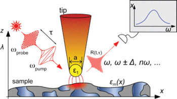
Figure 1: General setup for linear and non-linear tip-assisted optical spectroscopies. A sharp tip is brought into the optical near-field and illuminated from the side. The backscattered light from the tip-sample gap is detected in the far-field using a suitable detection scheme. For TERS the tip must be metallized so surface plasmons can be excited, which will then give rise to signal enhancement.
Tip-assisted Raman spectroscopy. The Raman signal from the sub-50 nm region associated with an AFM tip normally would be vanishingly small considering inefficiency of the Raman process in addition to the reduction of the collection area from several square-microns for a far-field illumination spot to a sub micron-square for a typical AFM tip. However, if one chooses a suitable combination of tip and incident light and places them in the correct geometry, a strong electromagnetic field is generated at the apex of the tip (see Figure 1). This field results from the incident light exciting a plasmon resonance in the tip.
This field can be enhanced by the combination of certain metal tips with particular excitation light sources—for example, a silver tip with green light and a gold tip with red light. Coinage metals work well as materials for tip-enhanced Raman scattering (TERS) tips because they exhibit a surface plasmon resonance in the visible range of the spectrum and thus can be excited by the incident laser beam. This strong enhancement is what makes Raman spectroscopy on the nanometer scale feasible [Reference Hartschuh7]. Incidently, a side illumination scheme as shown in Figure 1 has been shown to generate the highest enhancement factor for TERS [Reference Downes, Salter and Elfick8, Reference Yang, Aizpurua and Xu9]. Because of the strong localization of the electromagnetic field around the tip, TERS exhibits a much higher surface sensitivity than far-field Raman spectroscopy [Reference Stoeckle, Suh, Deckert and Zenobi10].
Raman is a directional process, and thus the polarization of the electromagnetic field along the tip axis has an effect on the selection rules for Raman emission. This can become important when comparing far-field and near-field data [Reference Ichimura, Fujii, Verma, Yano, Inouye and Kawata11]. The following experiment will demonstrate the importance of polarization control of the incident beam for TERS (Figure 2). An etched gold wire was used as a TERS tip and glued to a tuning fork. The tuning fork was operated at resonance so that the tip is oscillated at an amplitude of about 1 nm parallel to the surface. This non-optical feedback method is often referred to as shear-force feedback and keeps the tip in feedback approximately 3 nm above a sample [Reference Rensen12]. Using a waveplate, the incident light polarization is varied from being along the tip axis (p-polarized) to being perpendicular to the tip axis (s-polarized). The spectrum in Figure 2 shows the D- and G-band region of graphene from 1300 to 1600 cm−1, and one can see that the enhancement effect almost disappears when s-polarized illumination is used.
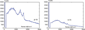
Figure 2: TERS of graphene obtained using a gold tip and tuning fork feedback. It is evident that the TERS effect only occured when the incident light was polarized along the tip axis (p-polarized) and not perpendicular to it (s-polarized). (The authors would like to thank Samuel Berweger, University of Colorado, for help in acquiring these spectra.)
Tip-enhanced spectroscopies such as TERS open the door to a whole new field of research. The improvement in spatial resolution is the obvious gain one expects from combining traditional far-field spectroscopies with AFM, but there also will be a higher sensitivity to surface features. The difference in selection rules between near- and far-field experiments indicates that TERS will be similar to conventional Raman spectroscopy but will not just yield the same information on a smaller length scale.
Instrumentation for a Combined AFM-Raman System
The biggest challenge in a combined instrument enabling Raman spectroscopy and nanoscale surface characterization is to avoid compromising the performance of either. Several design factors need to be considered.
Optical interference. Raman measurements are carried out using excitation in the visible regime. To allow parallel, simultaneous operation of the spectrometer and the AFM, the wavelength of the AFM beam-bounce system should be changed to the near-IR so as to not interfere with optical measurements. Alternatively, a non-optical feedback system such as STM or tuning fork feedback should be employed [Reference Rensen12].
Noise. Spectrometer systems often employ several lasers that may be cooled by noisy external fans or water cooling systems. They also may radiate heat in the proximity of the AFM. Both of these effects can negatively affect AFM performance. Noise from fans can couple into the AFM and cause instabilities in the feedback loop. Temperature changes will cause the sample to drift and make it extremely difficult to keep the tip in the selected field-of-view.
Measurement location. To operate without a compromise in performance, the sample could be shuttled between the AFM and the Raman spectrometer as shown in Figure 3 (upper images). However, to achieve true co-localized measurements providing the benefits of both the AFM's high spatial resolution and TERS, the sample should be scanned underneath the tip. This is because the laser beam exciting the plasmon resonance in the AFM tip must be focused on the tip during the imaging process, thus forcing the AFM imaging to be accomplished by sample scanning (Figure 3, lower).
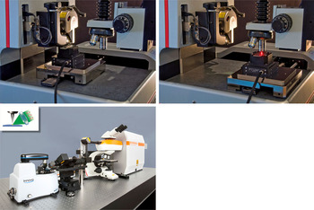
Figure 3: View of the Bruker Dimension Icon stage and optics arm of the Raman microscope for co-located AFM-Raman measurements (shown on top). The Icon stage shuttles the sample between the AFM head (left) and the Raman objective (right). The red spot emanating the objective is the Raman laser illuminating the sample during a Raman measurement. Sample-scanning Bruker Innova TERS setup (bottom). Here the Raman objective looks at the tip from the side, and AFM-Raman data are acquired simultaneously.
For certain non-TERS co-localized AFM and Raman measurements, that is, the execution of an AFM and micro-Raman experiment on the sample location, a tip-scanning AFM could be employed. These co-located measurements do not rely on the near-field enhancement of the AFM tip and are straightforward to perform and interpret because ScanAsyst® software automation can be used [Reference Kaemmer13]. However, these methods do not benefit from the resolution enhancement that TERS can provide.
Co-Localized AFM and Raman Measurements
Co-located AFM and Raman data acquisition can be accomplished in tip-scanning mode. This mode has many applications even though the spatial resolution of analysis is diffraction-limited.
Semiconductors. To better illustrate the results one can get with a co-located AFM-Raman setup, we start with a rather simple sample. The dataset depicted in Figure 4 shows a semiconductor structure with partially buried silicon. The sample topography acquired by AFM shows surface structures on the specimen but lacks chemical information. Chemical information is available in the Raman map on the right that is based on integration of the silicon peak at 520 cm−1. The areas in red, yellow, and green are exposed silicon.
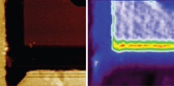
Figure 4: Simultaneous AFM-Raman acquisition sequence with (left) AFM sample topography and (right) Raman map. The Raman image was created by plotting the intensity of the main silicon band at 520 cm−1. The areas in red, yellow, and green depict the areas of exposed silicon. Image size is 30 μm.
Graphene. AFM and Raman are often used to study the material properties of graphene and carbon nanotubes [Reference Saito, Hoffmann, Dresselhaus, Jorio and Dresselhaus5]. Here we use the combination of quantitative nanomechanical measurements (QNM) and Raman spectroscopy to help better understand these materials. The intensity of the graphene G-band around 1580 cm−1 and the shape of the 2D band around 2700 cm−1 can be used as a measure of the number of layers. The intensity of the D-band around 1350 cm−1 indicates disorder of the lattice. Figure 5 shows AFM and Raman images of the G- and D-band of several graphene flakes prepared on silicon oxide. Correlations of the data unambiguously reveals the layered structure and the 300 pm step height between adjacent layers. The D-band image also hints at an area of increased defects along the edge of the single portion of the sample. This area was subsequently investigated using the QNM capabilities of the AFM. Figure 6 shows four channels (topography, adhesion, modulus, and deformation) of QNM data from a 2.5 μm scan size within the blue box of Figure 5. In the topographic map we can identify some wrinkle-like structures. These structures exhibit reduced adhesion and softer compliance (lower modulus) compared to the undisturbed portion of the layer. The deformation channel additionally shows a larger deformation on the graphene flake when compared to the substrate and allows us to deduce that the graphene flake does not mechanically relax during the sub-millisecond contact time of the QNM measurement. Thus, the combination of co-located AFM and Raman data has allowed us not only to easily find and identify relevant features on the sample but also to further investigate their mechanical behavior in detail.
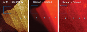
Figure 5: AFM topography (left) and Raman images of the G-band (middle) and D-band (right) of graphene flakes on silicon. Both Raman and AFM data confirm the layered structure with a 300 pm step height separating layers. The Raman image of the D-band also suggests an increased density of defects along the edge of the single layer. Image width = 15 μm. The area inside the blue box is shown at higher resolution in Figure 6.
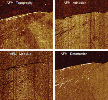
Figure 6: Simultaneously recorded quantitative nanomechanical AFM data of a single and double layer of graphene (within box of Figure 5). The wrinkles visible in the topography (top left) are reflected in the mechanical property channels as being softer (bottom left) and with less adhesion (top right) than the surrounding material. The deformation channel (bottom right) points to plastic deformation of the layers because they do not relax during the sub-millisecond contact time. Image width = 2.5 μm.
TERS Measurements
Higher spatial resolution of analysis is possible with TERS, and molecular studies are a major interest [Reference Steidtner and Pettinger14]. The following dataset depicts experiments on malachite green, a dye that has been used in the literature to demonstrate the single-molecule sensitivity of TERS [Reference Neascu, Dreyer, Behr and Raschke15]. Figure 7 shows sets of Raman spectra taken at different heights of the tip above the sample. With the tip in feedback, the spectrum, shown in red, nicely displays the characteristic bands that let one identify the functional groups of malachite green. With the sample just pulled away 60 nm, but the laser spot still focused onto the tip, it is evident that the TERS effect vanished and the spectrum, shown in black, is now purely generated by the far-field interaction. Both spectra were taken using the same integration time of 1 s. The ratio in intensity between the peak intensity in the near-field and far-field normalized to the different illumination areas is the TERS enhancement factor, which typically ranges from 104 to 108 depending on the combination of tip sample used in a specific experiment. These so-called tip checks are highly recommended in TERS to avoid the danger of getting a spectrum from material that the tip accidently picked up [Reference Domke and Pettinger16]. Another often-overlooked fact is that multiple scattering events between the metallic tip and the sample can give rise to a signal enhancement that is not caused by a near-field effect [Reference Ramos and Gordon17].
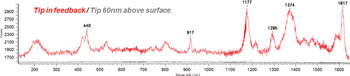
Figure 7: TERS spectra of malachite green obtained using a gold tip illuminated by 633 nm light at varying distances above the surface. The red spectrum was obtained with the tip in feedback, whereas the black spectrum was collected with the sample pulled 60 nm away from the tip (no TERS enhancement).
Besides careful polarization control, tip-sample approach curves, and good confocality of the Raman system employed, checking that the TERS signal changes reproducibly at distances well below the diffraction limit is another important step. This is shown in the experiment shown in Figure 8. After a topographic scan was taken, the tip was parked at the location indicated by the blue dot, and a TERS spectrum was acquired. Under closed-loop control, the tip was then moved to the location marked by the green dot, and another Raman spectrum was taken. To verify that no sample damage occurred, the tip was moved back to the original starting position, and another spectrum was recorded. The intensity changes in the spectra between the two locations demonstrate that the resolution is indeed sub-wavelength and that no sample or tip damage occurred during the data acquisition. Lateral resolution for TERS is related to the active area of the signal-enhancing tip and is somewhere in the range 10 nm–20 nm.
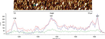
Figure 8: TERS of malachite green at two different locations separated by <90 nm indicated by the blue and green dots in the above SPM image. The first spectrum at location 1 is displayed in blue, the second spectrum at location 2 in green, and the third spectrum back at location 1 is shown in red. This figure demonstrates both sub-diffraction lateral spatial resolution and reproducibility of analysis.
Conclusion
Co-localized AFM and Raman instrumentation allows researchers to interrogate samples using both scanning probe techniques and optical spectroscopy, yielding detailed information about nanoscale properties and composition. Diffraction-limited AFM-Raman experiments are straightforward, as is the interpretation of data. Tip-enhanced Raman spectroscopy (TERS) provides chemical information on the nanometer scale. TERS experiments are straightforward to execute but may require special consideration of the tip-sample interaction in the optical near-field for data interpretation.


