


Introduction
Light elements are key constituents of many advanced materials and energy management technologies, for example, oxygen in dielectrics and superconductors, lithium in battery materials, and hydrogen in hydrogen storage materials. This makes the reliable imaging of light elements an important goal for atomic-resolution structure analysis. For preliminary, real-time exploration of unknown structures, imaging modes for which the structure can reliably be interpreted by visual inspection are essential. One particularly successful tool for atomic-resolution imaging is aberration-corrected scanning transmission electron microscopy (STEM), whereby a finely focused electron probe is scanned across a specimen and images are built up by plotting signals measured by various detectors as a function of probe position. The most established mode for directly interpretable atomic-resolution imaging in STEM is (high-angle) annular darkfield (ADF), shown schematically on the left in Figure 1, in which an annular detector collects electrons that have been scattered through large angles [Reference Pennycook and Jesson1]. In ADF images, atomic columns appear as peaks, the brightness of which scales strongly with the atomic number of the atoms in the column. This is evident in the experimental ADF images in Figure 1: the heavier Co, Ti, and Al columns are clearly visible, but the lighter O and Li columns are not. However, it has been demonstrated recently that both light and heavy elements are directly and robustly visible in atomic-resolution STEM images recorded using an annular detector in the outer area of the so-called bright-field region, that is, the portion of the diffraction plane that the unscattered beam would illuminate in the absence of a specimen [Reference Okunishi2, Reference Findlay3]. This is confirmed in the annular bright-field (ABF) images in Figure 1 in which the atomic columns appear as dark troughs: the locations of the O and Li columns are evident. This article gives a brief introduction to ABF imaging, including some examples of light-element imaging in crystal structures containing both light and heavy elements.
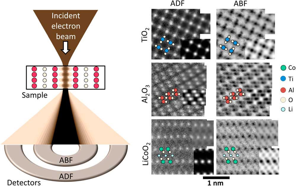
Figure 1 Left: schematic of a STEM probe scattering through a crystal and the ADF and ABF detector geometry. Right: Experimental ADF and ABF images of TiO2 [001] and Al2O3 [0 $\overline{1} $
0] for 200 keV electrons, a 22 mrad probe-forming aperture semiangle, and an 11–22 mrad ABF detector; and LiCoO2 [010] for 200 keV electrons, a 25 mrad probe-forming aperture semiangle, and a 6–25 mrad ABF detector. The main images show raw data. The upper insets show repeat-unit averages of the experimental data, while the lower insets show image simulations. The atomic structure models are also overlaid on each image.
$\overline{1} $
0] for 200 keV electrons, a 22 mrad probe-forming aperture semiangle, and an 11–22 mrad ABF detector; and LiCoO2 [010] for 200 keV electrons, a 25 mrad probe-forming aperture semiangle, and a 6–25 mrad ABF detector. The main images show raw data. The upper insets show repeat-unit averages of the experimental data, while the lower insets show image simulations. The atomic structure models are also overlaid on each image.
Materials and Methods
ABF versus ADF
An imaging mode is said to be robust and directly interpretable if a close correspondence between the appearance of the image and the specimen structure persists over a wide range of specimen thicknesses and is not overly sensitive to coherent aberrations in the lens. Figure 2 shows simulated tableaux of images for three different STEM imaging modes for a range of sample thicknesses and probe-forming lens defocus values. The assumed sample is LaAlO3, viewed along the [001] direction, using 200 keV electrons and a 23 mrad probe-forming convergence aperture semi-angle. Other parameters are given in the figure caption. This ADF imaging is seen to be robust: the images have the same, directly interpretable form, with bright peaks on the atomic columns, over a wide range of thickness values and a moderate range of defocus values. By contrast, the appearance of bright-field (BF) images formed with a small, on-axis disk detector is seen to be very sensitive to sample thickness and probe defocus: BF imaging is not robust. The ABF images, however, are seen to be robust, consistently showing dark troughs on the atomic columns over a wide range of thicknesses, albeit for a slightly narrower range of defocus values than ADF.
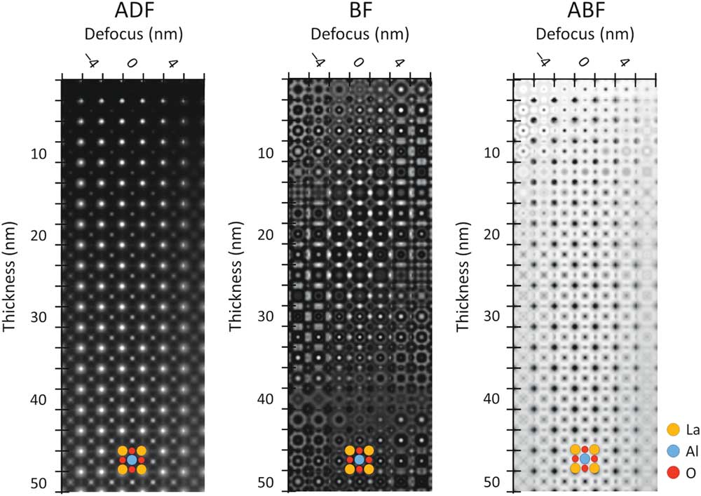
Figure 2 Simulated tableaux for LaAlO3 [001] showing how the appearance and contrast of ADF, BF, and ABF images vary over a range thickness and defocus values. Assumed conditions are 200 keV electrons and a 23 mrad probe-forming aperture semi-angle. The detector ranges are: ADF 81-228 mrad, BF 0-0.5 mrad, and ABF 11.5-23 mrad. The atomistic structure is overlaid.
Image formation in ABF
While scattering of fine electron probes through materials is a highly complex process in detail, the general form and robustness of ABF images follows because the behavior shown schematically in Figure 3 is a reasonable “first order” description for atomically-fine fast electron probes scattering through well-aligned crystal specimens. The distribution of scattered electrons remains fairly uniform when the probe is positioned between columns, as shown in the left panel in Figure 3. Elastic scattering tends to forward-focus the electron probe when it is placed on columns of light elements, as shown in the central panel in Figure 3 [Reference Findlay3, Reference Findlay4]. Thermal scattering tends to scatter the electron probe to high angles when it is placed on columns of heavy elements, as shown in the right panel in Figure 3 [Reference Findlay4]. Because both of these distinct image-forming mechanisms—forward-focusing by light element columns and high-angle scattering by heavy-element columns—reduce the electron intensity in the outer area of the bright-field region relative to its value when the probe is between columns, both light and heavy atomic columns appear consistently as dark spots in ABF images, making ABF images directly interpretable. Because the intensity reduction caused by these two distinct image-forming mechanisms is of comparable magnitude, light elements are generally visible even when much heavier elements are present. It should be noted that the idea of using an annular detector in the bright-field region has a long history [Reference Rose5–Reference Cowley8]. However, it is the recent appreciation of the relatively robust dynamics afforded for atomically fine electron probes channeling along columns, as described above, which has led to the wide uptake of ABF imaging for materials science investigations.
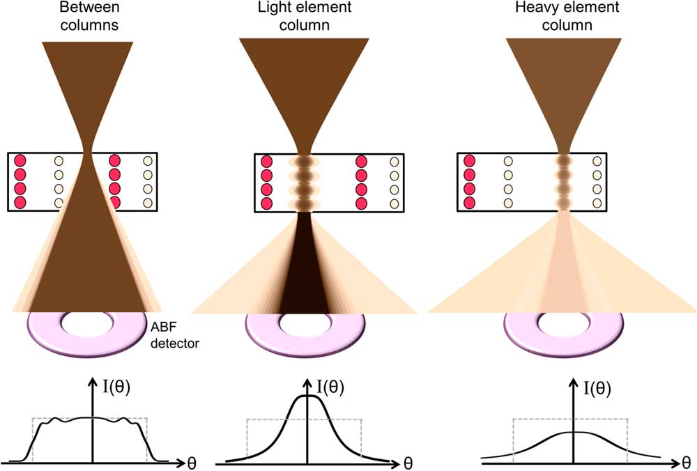
Figure 3 Upper: Conceptual sketch indicating the rough angular distribution of scattered electrons when the probe is between columns (left), on top of a light-element column (middle), and on top of a heavy-element column (right), with shade indicating electron density. Lower: Corresponding profiles through the diffraction pattern as a function of scattering angle. The dashed line is the top-hat distribution that would occur in the absence of a specimen.
STEM detector setup
A detailed analysis of the dynamics of ABF imaging has been published [Reference Findlay3, Reference Findlay4, Reference Lugg9, Reference Findlay10]. Here we will simply summarize some of the findings. Imaging in ABF mode relies on a reasonable coupling between the electron probe and the atomic columns, and so, unlike ADF, this imaging mode is restricted to atomic-resolution imaging. As a good rule-of-thumb, if the probe-forming aperture semiangle is α then the ABF detector should span the range α/2 to α. Many microscopes have an annular detector of suitable proportions, but if such is not available then one could use a disk detector in conjunction with a beam stop, or else an annular detector with different proportions in conjunction with an aperture. While we have found no systematic advantage for varying the detector inner and outer angles relative to the rule-of-thumb guide, there is also little penalty for modest variations in these angles. All other things being equal, higher accelerating voltages tend to give better ABF contrast [Reference Lugg9], though the effect is small and in practice must be balanced against other considerations such as beam damage.
Atomic column intensities
A monotonic relationship between atomic number and ABF trough depth is not guaranteed [Reference Findlay3], though relative reversals—where the trough depth of a light-element column is deeper than that of a heavy-element column—are not the norm. A more nuanced statement would note that the relevant quantity for comparison is not simply the element type, but rather the projected atomic number density; an oxygen-column trough would probably be deeper than an aluminum-column trough if there were twice as many oxygen atoms as aluminum atoms for the same thickness. Genuine contrast reversal in ABF imaging—where columns become bright peaks rather than dark troughs—can occur in extremely thin specimens (less than a few nm in thickness) [Reference Lee11, Reference Phillips and Klie12]. Note, however, that STEM allows for the simultaneous recording of an ADF image, and with the information from both ABF and ADF images we have not come across any genuine ambiguity in structure interpretation.
Results
Grain boundaries
ABF imaging is most effective when the spacing between columns is large. If the inter-column spacing is very small, roughly an angstrom (0.1 nm) or less, the location of the trough minima may be displaced somewhat from the true column locations [Reference Findlay3], an effect that also occurs in ADF [Reference Hovden13]. ABF imaging relies on electron scattering along columns and so is not suited to amorphous samples. However, for small perturbations away from crystalline order, such as mild static disorder or a small number of dopants/vacancies, ABF tends to be more robust than ADF [Reference Findlay3]. This is seen in Figure 4, which shows simultaneously recorded ADF and ABF images of a Σ13 grain boundary in α-Al2O3. In the ADF image, the contrast at the grain boundary is much lower than that in the bulk, obscuring the interface structure. It has been speculated that this is a consequence of vacancy segregation to the boundary and the associated distortions that come from structural relaxation of the atoms surrounding a vacancy [Reference Findlay14, Reference Lee15]. However, the grain boundary structure is much clearer in the ABF image, to the extent that individual O columns are evident in the grain boundary itself [Reference Findlay14].
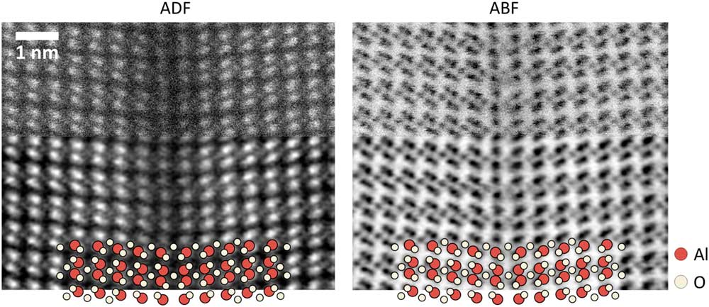
Figure 4 ADF and ABF images of a ∑13 [1 $\overline{1} $
10] (10
$\overline{1} $
4) grain boundary in α–Al2O3. The upper portion shows the raw data, while the lower portion shows the data after a radial difference filter as released by HREM Inc. [27] has been applied. The atomistic structure is overlaid. Note that the oxygen columns in the grain boundary are visible in the ABF image.
$\overline{1} $
10] (10
$\overline{1} $
4) grain boundary in α–Al2O3. The upper portion shows the raw data, while the lower portion shows the data after a radial difference filter as released by HREM Inc. [27] has been applied. The atomistic structure is overlaid. Note that the oxygen columns in the grain boundary are visible in the ABF image.
Light-element atomic columns
ABF has proven useful for visualizing oxygen columns in ceramics and nitrogen columns in semiconductors, and for these elements ABF imaging is quite robust. ABF imaging of still lighter elements is possible. ABF has been successfully applied to visualizing boron [Reference Findlay4, Reference Lazar16], lithium [Reference Oshima17, Reference Huang18] and hydrogen [Reference Findlay19, Reference Ishikawa20] within crystalline environments. However, for these lightest of elements the imaging remains challenging: direct interpretation may apply only over a restricted range of thicknesses, the signal can be of similar magnitude to the noise level, and the specimens tend to damage under the beam. All other things being equal, ABF contrast is most clearly visible when the inter-atomic spacing along the column is small while the inter-column spacing in the image is large. Thus for imaging very light elements, for example, lithium and hydrogen, some materials are more amenable to ABF imaging than others. Figure 5 shows simulated ABF images for a range of Li-bearing compounds for which the inter-atomic spacing along the column is appreciably different. It is seen that the Li-columns are most visible in LiCoO2 [010], where the space between Li atoms along the column is only 2.8 Å, whereas they are least visible in LiMn2O4 [110], where the space between Li atoms along the column is 5.8 Å.
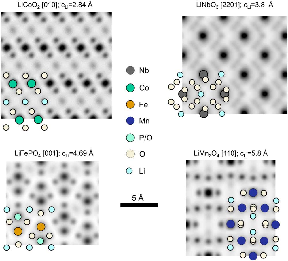
Figure 5 Simulated ABF images for a set of Li-containing compounds selected to show that lithium is more visible when the along-column interatomic distance between Li atoms, c, is smaller. The simulations assume 200 keV electrons, a 25 mrad probe-forming aperture semiangle, and an ABF detector spanning the range 12.5–25 mrad. The atomistic structure is overlaid.
Enhanced ABF
In our discussion above on the scattering behavior shown schematically in Figure 3, we concentrated on the behavior in the outer portion of the bright-field region. However, the schematic can also be used to understand the signal recorded on a disk detector complementary to the ABF detector within the bright-field region: a light-element column should appear bright, since the forward focusing peaks up the intensity in this region; a heavy-element column should appear dark, since thermal scattering reduces the intensity in this region. Kotaka and co-workers [Reference Ohtsuka21, Reference Kotaka22] refer to this imaging mode as middle-angle bright-field (MaBF) imaging and offer it as a means to enhance resolution—the contrast reversal between light and heavy elements makes their positions easier to determine—and a way of highlighting the light-element positions by forming color-composite images using both MaBF and ADF signals. If both ABF and MaBF images are recorded, subtracting one from the other serves to preferentially enhance the visibility of light elements relative to heavy elements to a greater extent than in ABF imaging alone, and the resulting imaging mode has thus been referred to as enhanced ABF (eABF) imaging [Reference Findlay23]. This is evident in Figure 6, which shows ADF, ABF, MaBF, and eABF for a SrTiO3 sample viewed along the [001] orientation.
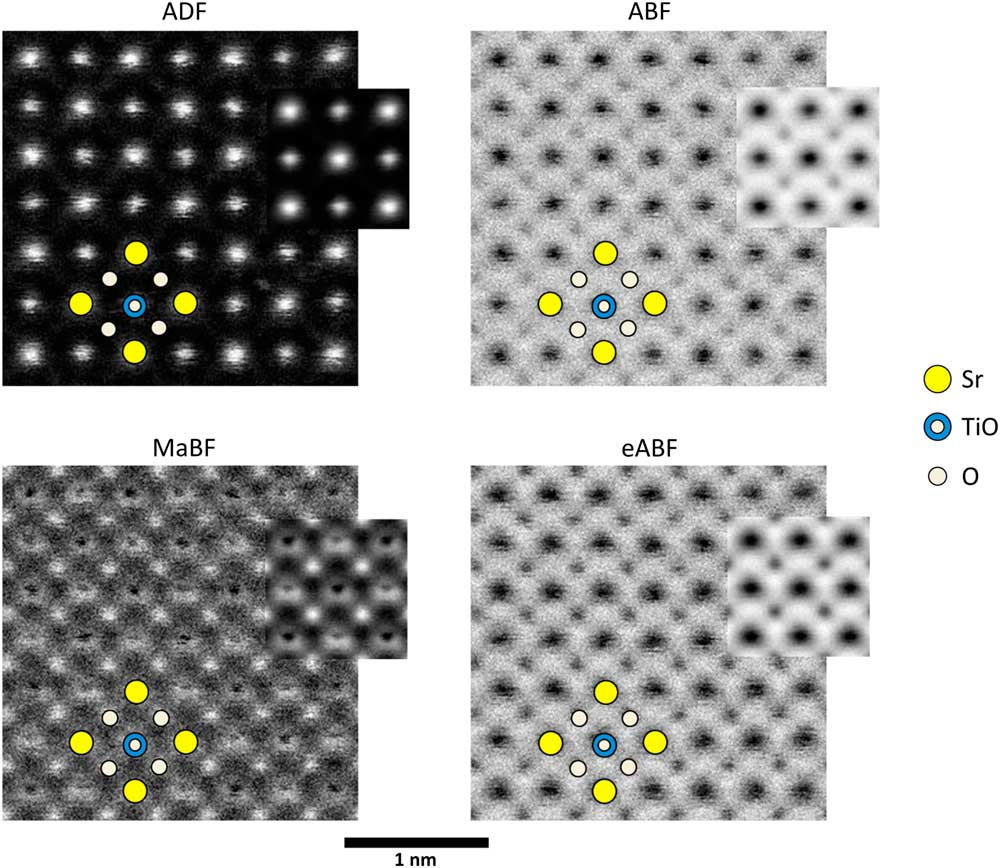
Figure 6 ADF, ABF, MaBF, and eABF images of SrTiO3 [001] for 300 keV electrons and a 24 mrad probe-forming aperture semi-angle. The ABF detector spans the range 12–24 mrad. The MaBF detector spans the range 0–12 mrad. The insets show repeat-unit averages of the experimental data. The atomistic structure is overlaid.
Other applications
With a few exceptions [Reference Lee24], ABF imaging is of questionable use for quantitative analysis based on image intensity. However, it is proving itself highly useful for cases where visualization of the location of light columns is informative, such as determining the range over which the rotation of oxygen octahedra varies in the vicinity of an interface [Reference Aso25] and the structural changes that occur through the charge/discharge cycle of lithium battery materials [Reference Sun26]. ABF images can be recorded simultaneously with STEM ADF images and also with some spectroscopic imaging modes.
Conclusion
ABF imaging uses the scattered electron intensity at the outer portion of the bright-field disk to image both light and heavy atomic columns simultaneously. By providing directly and robustly interpretable images, it can be used in real time as a tool for discovery when exploring unknown samples. This method is straightforward to implement on the majority of modern aberration-corrected scanning transmission electron microscopes.
Acknowledgments
The authors thank all their collaborators in developing and applying ABF imaging. This research was supported under the Discovery Projects funding scheme of the Australian Research Council (Project No. DP140102538). A part of this work was conducted in Research Hub for Advanced Nano Characterization, The University of Tokyo, under the support of “Nanotechnology Platform” (project No.12024046) by MEXT, Japan.


