Hostname: page-component-8448b6f56d-m8qmq Total loading time: 0 Render date: 2024-04-25T02:33:39.651Z Has data issue: false hasContentIssue false

Three Dimensional Visualization of Electromagnetic Fields from One Dimensional Nanostructures

Published online by Cambridge University Press:  23 September 2015

Charudatta Phatak
Affiliation:
Materials Science Division, Argonne National Laboratory, Lemont, IL 60439, USA
Aurelien Masseboeuf
Affiliation:
CEMES-CNRS, 29, rue Jeanne Marvig, FR - 31055 Toulouse, France
Ludvig de Knoop
Affiliation:
CEMES-CNRS, 29, rue Jeanne Marvig, FR - 31055 Toulouse, France
Christophe Gatel
Affiliation:
CEMES-CNRS, 29, rue Jeanne Marvig, FR - 31055 Toulouse, France Universite Paul Sabatier, F-31000 Toulouse, France.
Martin J. Hytch
Affiliation:
CEMES-CNRS, 29, rue Jeanne Marvig, FR - 31055 Toulouse, France

Abstract

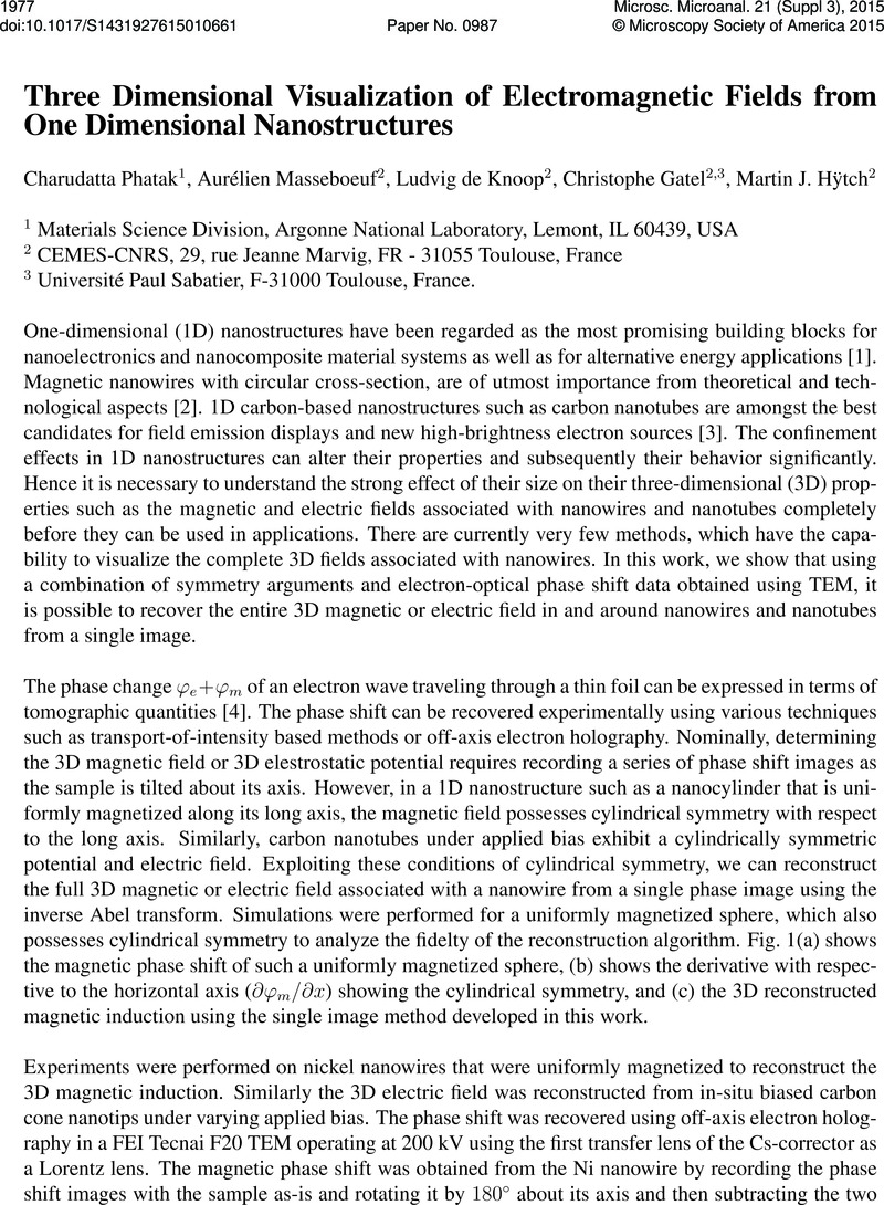
Image of the first page of this content. For PDF version, please use the ‘Save PDF’ preceeding this image.'
Type
Abstract
Copyright
Copyright © Microscopy Society of America 2015 

References

[1] Lieber, C. M., Solid State Communications 107, 607 (1998).CrossRefGoogle Scholar
[2] Chappert, C., Fert, A. & Van Dau, F. N., Nature Materials 6, 813 (2007).Google Scholar
[3] de Jonge, N., Lamy, Y., Schoots, K. & Oosterkamp, T. H., Nature 420, 393 (2002).Google Scholar
[4] Phatak, C., Beleggia, M. & De Graef, M., Ultramicroscopy 108, 503 (2008).Google Scholar
[5] This work was support by U.S. Department of Energy (DOE), Office of Science, Materials Sciences and Engineering Division.Google Scholar