Hostname: page-component-848d4c4894-pjpqr Total loading time: 0 Render date: 2024-06-24T02:10:19.312Z Has data issue: false hasContentIssue false

Etching and Mending of Graphene Edges by Cu and Pt Atoms

Published online by Cambridge University Press:  04 August 2017

Emi Kano
Affiliation:
Graduate School of Pure and Applied Sciences, University of Tsukuba, Tsukuba, Japan In-situ Characterization Technique Development Group, National Institute for Materials Science, Tsukuba, Japan
Ayako Hashimoto
Affiliation:
Graduate School of Pure and Applied Sciences, University of Tsukuba, Tsukuba, Japan In-situ Characterization Technique Development Group, National Institute for Materials Science, Tsukuba, Japan Global Research Center for Environment and Energy based on Nanomaterials Science, National Institute for Materials Science, Tsukuba, Japan Transmission Electron Microscopy Station, National Institute for Materials Science, Tsukuba, Japan
Masaki Takeguchi
Affiliation:
Graduate School of Pure and Applied Sciences, University of Tsukuba, Tsukuba, Japan In-situ Characterization Technique Development Group, National Institute for Materials Science, Tsukuba, Japan Transmission Electron Microscopy Station, National Institute for Materials Science, Tsukuba, Japan

Abstract

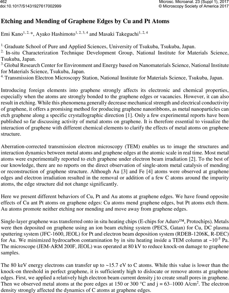
Image of the first page of this content. For PDF version, please use the ‘Save PDF’ preceeding this image.'
Type
Abstract
Copyright
© Microscopy Society of America 2017 

References

[1] Datta, S. S., et al., Nano Lett. 8 2008 19121915.Google Scholar
[2] Ramasse, Q. M., et al., ACS Nano 6 2012 40634071.Google Scholar
[3] Wang, H., et al., Nanoscale 4 2012 29202925.Google Scholar
[4] Zhao, J., et al., Proc. Natl. Acad. Sci. 111 2014 1564115646.Google Scholar
[5] Kano, E., et al., Nanoscale 8 2016 529535.Google Scholar
[6] A part of this work was supported by “Nanotechnology Platform Project” of the Ministry of Education, Culture, Sports, Science and Technology (MEXT), Japan, and JSPS KAKENHI Grant Numbers 15J04118, 25390035 and 16H03875, Japan.Google Scholar
[7] First author will move after the graduation: National Institute of Nanotechnology, 11421 Saskatchewan Drive, Edmonton, Canada.Google Scholar