Hostname: page-component-848d4c4894-8kt4b Total loading time: 0 Render date: 2024-07-07T03:44:04.258Z Has data issue: false hasContentIssue false

Assessing Hexagonal Boron Nitride Crystal Quality by Defect Sensitive Etching

Published online by Cambridge University Press:  04 August 2017

T. Hoffman
Affiliation:
Dept of Chemical Engineering, Kansas State University, Manhattan, Kansas, USA
Y. Zhang
Affiliation:
Dept of Chemical Engineering, Kansas State University, Manhattan, Kansas, USA
S. Liu
Affiliation:
Dept of Chemical Engineering, Kansas State University, Manhattan, Kansas, USA
N. Khan
Affiliation:
School of Science and Technology, Georgia Gwinnett College, Lawrenceville, Georgia, USA
M.E. Twigg
Affiliation:
United States Naval Research Laboratory, Washington, DC, USA
N.D. Bassim
Affiliation:
Dept of Materials Science and Engineering, JHE 357, McMaster University, Hamilton, Ontario, CANADA
J.H. Edgar
Affiliation:
Dept of Chemical Engineering, Kansas State University, Manhattan, Kansas, USA

Abstract

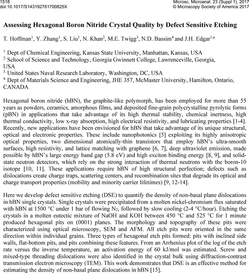
Image of the first page of this content. For PDF version, please use the ‘Save PDF’ preceeding this image.'
Type
Abstract
Copyright
© Microscopy Society of America 2017 

References

[1] Paine, R.T. & Narula, C.K. Chem. Rev 90, 73 1990.CrossRefGoogle Scholar
[2] Moore, A.W. J. Cryst. Growth 106, 6 1990.Google Scholar
[3] Perkins, R.T. Adv. X-Ray Anal 33, 625 1990.Google Scholar
[4] Pease, R.S. Acta Crystallogr 5, 356 1952.Google Scholar
[5] Austerman, S.B., Myron, S.M. & Wagner, J.W. Carbon 5, 549 1967.Google Scholar
[6] Dean, C.R., et al, Nat. Nanotechnol 5, 722 2010.Google Scholar
[7] Arnaud, B., et al, Phys. Rev. Lett 96, 932 2006.Google Scholar
[8] Kubota, Y., et al, Science 317, 932 2007.Google Scholar
[9] Kubota, Y., et al, Chem. Mater 20, 1661 2008.CrossRefGoogle Scholar
[10] McGregor, D.S., Unruh, T.C. & McNeil, W.J. Nucl. Instrum. Meth. A 591, 530 2008.Google Scholar
[11] Doan, T.C., et al, Nucl. Instrum. Meth. A 591, 121 2015.Google Scholar
[12] Huang, J. & Zhu, Y.T. Defect Diffus, Forum 186–7, 1 2000.Google Scholar
[13] Turan, S. & Knowles, K.M. Phys. Status Solidi A 150, 227 1995.Google Scholar
[14] Weyher, J.L. & Kelly, J.J. Defect-selective etching of semiconductors. Springer Handbook of Crystal Growth, 14531476, 2010.Google Scholar
[15] The authors acknowledge Dr. Tina Salquero in University of Georgia for the use of Innova AFM for surface studies. This work was supported by US Department of Homeland Security and National Science Foundation under the Academic Research Initiative program (Award No: 2011-DN-077- ARI048-03).Google Scholar