


Introduction
The fields of materials development and analysis have recently begun to explore the possibility of applying data-driven strategies and artificial intelligence (AI) for accelerating or automating a variety of tasks (Ong et al., Reference Ong, Richards, Jain, Hautier, Kocher, Cholia, Gunter, Chevrier, Persson and Ceder2013; O'Mara et al., Reference O'Mara, Meredig and Michel2016; Dagdelen et al., Reference Dagdelen, Montoya, De Jong and Persson2017; Ward et al., Reference Ward, Dunn, Faghaninia, Zimmermann, Bajaj, Wang, Montoya, Chen, Bystrom, Dylla, Chard, Asta, Persson, Snyder, Foster and Jain2018; Ziletti et al., Reference Ziletti, Kumar, Scheffler and Ghiringhelli2018; Avery et al., Reference Avery, Wang, Oses, Gossett, Proserpio, Toher, Curtarolo and Zurek2019; DeCost et al., Reference DeCost, Lei, Francis and Holm2019; Oviedo et al., Reference Oviedo, Ren, Sun, Settens, Liu, Hartono, Ramasamy, DeCost, Tian, Romano, Gilad Kusne and Buonassisi2019; Tshitoyan et al., Reference Tshitoyan, Dagdelen, Weston, Dunn, Rong, Kononova, Persson, Ceder and Jain2019; Dunn et al., Reference Dunn, Wang, Ganose, Dopp and Jain2020; Kaufmann & Vecchio, Reference Kaufmann and Vecchio2020; Kaufmann et al., Reference Kaufmann, Maryanovsky, Mellor, Zhu, Rosengarten, Harrington, Oses, Toher, Curtarolo and Vecchio2020a, Reference Kaufmann, Zhu, Rosengarten and Vecchio2020d; Stan et al., Reference Stan, Thompson and Voorhees2020; Chen et al., Reference Chen, Zuo, Ye, Li and Ong2021). Computer vision is a subset of AI with the goal of training computers to understand the visual world and potentially act on that information (Zhu et al., Reference Zhu, Kaufmann and Vecchio2020a, Reference Zhu, Wang, Kaufmann and Vecchio2020b). Deep learning algorithms enable many computer vision applications and are of particular interest owing to their excellent performance without significant feature engineering (LeCun et al., Reference LeCun, Bengio and Hinton2015). While it can be difficult to precisely determine how and why these “black-box algorithms” are capable of performing these tasks, these methods can automate routine tasks, improve upon existing solutions, or provide understanding (Adadi & Berrada, Reference Adadi and Berrada2018; Holm, Reference Holm2019). While deep learning provides significant opportunities for the advancement of materials science, robust application of these tools requires an understanding of the conditions under which optimal performance is achieved. Unlike most cases involving natural images (Deng et al., Reference Deng, Dong, Socher, Li, Li and Fei-Fei2010), scientific images are less likely to be collected utilizing a wide range of parameters. For instance, micrographs may be captured with only 1 or 2 magnifications, while photographs of animals at different distances and from different angles are typically abundant (Deng et al., Reference Deng, Dong, Socher, Li, Li and Fei-Fei2010). Moreover, the knowledge of the conditions for which a model fails can guide the future collection of labeled training data to improve subsequent versions. However, in the context of electron diffraction, there likely exists some cases (e.g., no frame averaging) where reduced quality or lack of sufficient information in the images may limit performance regardless of training data available for a given technique.
Convolutional neural networks (CNNs) are the current standard deep learning models for processing image data (LeCun et al., Reference LeCun, Bengio and Hinton2015). Before a CNN can be applied to a given task, it must learn to assign importance to various aspects of the image that maximize the network's differentiation capabilities. In doing so, deep learning methods glean intricate functions of the inputs that are sensitive to minute details, yet ignore irrelevant information such as backgrounds (LeCun et al., Reference LeCun, Bengio and Hinton2015). However, it should be noted that it is only with careful design of a training set and rigorous validation that practitioners can be confident that the model has truly learned relevant information, is robust to new conditions, and has not found an unscientific approach to solving the problem [such as learning the presence of a ruler means a lesion is more likely cancerous (Esteva et al., Reference Esteva, Kuprel, Novoa, Ko, Swetter, Blau and Thrun2017)] (Zech et al., Reference Zech, Badgeley, Liu, Costa, Titano and Oermann2018; Riley, Reference Riley2019). The application of these tools to image-based tasks in materials science has proved to be useful for classification (Modarres et al., Reference Modarres, Aversa, Cozzini, Ciancio, Leto and Brandino2017; Ziletti et al., Reference Ziletti, Kumar, Scheffler and Ghiringhelli2018; Foden et al., Reference Foden, Collins, Wilkinson and Britton2019a; Kaufmann et al., Reference Kaufmann, Maryanovsky, Mellor, Zhu, Rosengarten, Harrington, Oses, Toher, Curtarolo and Vecchio2020a), segmentation (DeCost et al., Reference DeCost, Lei, Francis and Holm2019; Stan et al., Reference Stan, Thompson and Voorhees2020), and other objectives (Xie & Grossman, Reference Xie and Grossman2018; de Haan et al., Reference de Haan, Ballard, Rivenson, Wu and Ozcan2019). Examples of techniques where interest in developing artificial intelligence agents for image-based tasks include optical microscopy (DeCost & Holm, Reference DeCost and Holm2015; DeCost et al., Reference DeCost, Lei, Francis and Holm2019), scanning transmission electron microscopy (STEM) (Laanait et al., Reference Laanait, He and Borisevich2019; Roberts et al., Reference Roberts, Haile, Sainju, Edwards, Hutchinson and Zhu2019), transmission electron microscopy (TEM) (Spurgeon et al., Reference Spurgeon, Ophus, Jones, Petford-Long, Kalinin, Olszta, Dunin-Borkowski, Salmon, Hattar, Yang, Sharma, Du, Chiaramonti, Zheng, Buck, Kovarik, Penn, Li, Zhang, Murayama and Taheri2020), and electron backscatter diffraction (EBSD) (Shen et al., Reference Shen, Pokharel, Nizolek, Kumar and Lookman2019; Ding et al., Reference Ding, Pascal and De Graef2020; Kaufmann et al., Reference Kaufmann, Maryanovsky, Mellor, Zhu, Rosengarten, Harrington, Oses, Toher, Curtarolo and Vecchio2020a, Reference Kaufmann, Zhu, Rosengarten, Maryanovsky, Harrington, Marin and Vecchio2020b, Reference Kaufmann, Zhu, Rosengarten, Maryanovsky, Wang and Vecchio2020c). These efforts are motivated by accelerating data generation rates and the traditional need for tedious or arduous analysis of the data by well-trained individuals with sufficient knowledge of the material domain. Thus, it is important that these tools can be applied robustly as imaging parameters are varied to prevent increasing, instead of alleviating, researcher workloads. While different diffraction techniques often use distinct terminology, parameters such as accelerating voltage or detector distance are common among them and have similar effects on the collected diffraction patterns. Several of these parameters play a role in the amount of time required to collect each diffraction pattern and therefore complete the analysis of a sample. In this work, the EBSD technique is used owing to the relatively high rate of data collection and ease of changing each parameter.
EBSD is a scanning electron microscope (SEM)-based method that involves the capture of 2D diffraction patterns produced from an incident electron beam scattering, diffracting, and escaping from a well-polished “bulk” sample (Schwartz et al., Reference Schwartz, Kumar, Adams and Field2009). Despite the vast amount of information in the patterns (Vecchio & Williams, Reference Vecchio and Williams1987, Reference Vecchio and Williams1988; Schwartz et al., Reference Schwartz, Kumar, Adams and Field2009), conventional EBSD has primarily focused on determining three-dimensional orientation (Schwartz et al., Reference Schwartz, Kumar, Adams and Field2009; Thomsen et al., Reference Thomsen, Schmidt, Bewick, Larsen and Goulden2013; Tong et al., Reference Tong, Knowles, Dye and Britton2019; Zhu et al., Reference Zhu, Wang, Kaufmann and Vecchio2020b). Furthermore, the technique typically relies on a user-defined phase list and Hough-based indexing (Lassen, Reference Lassen1994). Hough-based indexing generally allows for phase differentiation of sufficiently distinct crystal structures (Britton et al., Reference Britton, Maurice, Fortunier, Driver, Day, Meaden, Dingley, Mingard and Wilkinson2010; Foden et al., Reference Foden, Previero and Britton2019b; Hielscher et al., Reference Hielscher, Bartel and Britton2019), but the process remains susceptible to structural misclassification (McLaren & Reddy, Reference McLaren and Reddy2008; Chen & Thomson, Reference Chen and Thomson2010; Karthikeyan et al., Reference Karthikeyan, Dash, Saroja and Vijayalakshmi2013). Improvements to phase differentiation have been proposed and developed including dictionary indexing (Chen et al., Reference Chen, Park, Wei, Newstadt, Jackson, Simmons, De Graef and Hero2015; Ram et al., Reference Ram, Wright, Singh and De Graef2017; Ram & De Graef, Reference Ram and De Graef2018; Singh et al., Reference Singh, Guo, Winiarski, Burnett, Withers and De Graef2018) and spherical indexing (Day, Reference Day2008; Lenthe et al., Reference Lenthe, Singh and De Graef2019; Zhu et al., Reference Zhu, Kaufmann and Vecchio2019), although each still requires a user to pre-select phases and further requires simulating the Kikuchi sphere for each selected phase. Recently, the EBSD community has begun to investigate the use of CNNs for indexing, phase differentiation, and determining components of the crystal structure (Foden et al., Reference Foden, Collins, Wilkinson and Britton2019a; Ding et al., Reference Ding, Pascal and De Graef2020; Kaufmann et al., Reference Kaufmann, Maryanovsky, Mellor, Zhu, Rosengarten, Harrington, Oses, Toher, Curtarolo and Vecchio2020a, Reference Kaufmann, Zhu, Rosengarten, Maryanovsky, Harrington, Marin and Vecchio2020b, Reference Kaufmann, Zhu, Rosengarten, Maryanovsky, Wang and Vecchio2020c). It is a goal of several of these efforts that the onus of phase selection and/or structure determination can be at least partially lessened on the user (Kaufmann et al., Reference Kaufmann, Maryanovsky, Mellor, Zhu, Rosengarten, Harrington, Oses, Toher, Curtarolo and Vecchio2020a, Reference Kaufmann, Zhu, Rosengarten, Maryanovsky, Harrington, Marin and Vecchio2020b). However, to date, there has not been a systematic study of CNN performance when the EBSD patterns (EBSPs) are collected using different experimental geometry than was used during collection or simulation of the training data. The knowledge of how these changes to the diffraction patterns influence proper pattern identification is paramount to widespread adoption of these machine-learning-based techniques.
This work seeks to develop an understanding of model performance as several of the most common EBSD operating conditions are varied. The specific parameters are frame averaging, detector tilt, sample-to-detector distance, accelerating voltage, and pattern resolution. With regard to parameters that directly affect the time to collect each pattern and therefore complete a map, such as frame averaging and pattern resolution, the ability to collect the data more rapidly without a significant reduction in performance is of interest. With respect to parameters such as detector tilt, it is important to determine if the model is susceptible to minor or major changes in the training conditions. Parameters such as detector distance and accelerating voltage can cause much more dramatic changes to the EBSPs, and it is, therefore, necessary to assess their influence. The CNN model tested in this work was trained to classify EBSPs to one of six space groups using patterns collected from a fixed EBSD setup (Kaufmann et al., Reference Kaufmann, Zhu, Rosengarten and Vecchio2020d). The effect of changing these parameters is tested using new EBSPs collected from one material from each space group and a dual-phase 2205 duplex steel for visual demonstration. Each time one parameter is varied, the EBSPs are re-collected, and the CNN used to reassess the proper space group identification. Ultimately, the model is found to retain a high classification accuracy even with significant changes to the diffraction conditions and therefore the EBSPs.
Materials and Methods
Materials
Eighteen different single-phase materials, comprising six of the ten space groups within the  $( {4/m\;\bar{3}\;2/m} )$ point group were selected for training the space group classification CNN. The space groups are $Pm\bar{3}m\;( {221} )$, $Pm\bar{3}n\;( {223} )$, $Fm\bar{3}m\;( {225} )$, $Fd\bar{3}m\;( {227} )$, $\;Im\bar{3}m\;( {229} )$, and $\;Ia\bar{3}d\;( {230} )$. Suitable samples for the remaining four space groups could not be obtained. The materials were [221: FeAl, NiAl, Ni3Al, Fe3Ni], [223: Cr3Si, Mo3Si], [225: Ni, Al, NbC, TaC, TiC], [227: Si, Ge], [229: W, Ta, Fe], and [230: Al4CoNi2, and Al4Ni3]. The collected diffraction patterns from these materials were of low texture, typically less than two times random in any direction. Refer to Kaufmann et al. (Reference Kaufmann, Zhu, Rosengarten and Vecchio2020d) for the distributions of orientation, band contrast, and mean angular deviation for these samples.
A dual-phase material with phases that are easily differentiable by Hough-based EBSD was used to visually demonstrate and compare the classification accuracy of the model as parameters vary. A longitudinal cross-section of cold-worked 2205 duplex steel was mounted, ground, and polished to 0.05 μm using colloidal silica. Looking at the longitudinal cross-section, cold-worked 2205 duplex stainless steel has a ferrite matrix (space group 229) and elongated austenite islands (space group 225) (Momeni et al., Reference Momeni, Dehghani and Zhang2012).
Electron Backscatter Diffraction Pattern Collection
EBSPs were collected in a Thermo Scientific (formerly FEI) Apreo scanning electron microscope (SEM) equipped with an Oxford Symmetry EBSD detector.
All EBSPs utilized in training were collected with the following fixed geometry. The EBSD detector was utilized in high-resolution (1,244 × 1,024) mode, the working distance was 18.1 ± 0.1 mm, the sample-to-detector distance was 19.1 mm, and the detector arm tilt set to 13.7° above horizontal. The imaging parameters for the training set EBSPs were 20 kV accelerating voltage, 51 nA beam current, and 30-pattern averaging. This fixed geometry and set of imaging parameters will be referred to as the “default” operating conditions. Refer to Figure 1 for an annotated image of the diffraction setup in the SEM.

Fig. 1. EBSD setup and variable parameters. An annotated view of the EBSD setup. Parameters that vary in this study are listed below the equipment label. The sample-to-detector distance (DD) and detector tilt (DT) are further detailed by arrows describing their function. Detector tilt is defined as the angle between the detector arm and horizontal.
Diffraction patterns from six single-phase materials (Ni3Al, Cr3Si, TiC, Si, Fe, and Al4CoNi2) and the dual-phase 2205 duplex steel were collected separately from the training data to determine a baseline accuracy for the model when using the default diffraction geometry. Approximately 3,000 individual patterns were collected from a large area of each sample (i.e., low magnification) to capture as many unique orientations as possible over the fixed region. After collecting data using the default diffraction geometry, each one of the parameters was systematically varied one at a time and the same ~3,000 patterns re-collected from the same location.
The parameters were varied as follows. Frame averaging was set to 1, 5, 10, 20, or 30. The software detector tilt below zero ranged from 1 to 5 in steps of 1. These values correspond to the detector arm being 14.2°, 14.0°, 13.7°, 13.5°, and 13.3° above the horizontal plane. The software detector insertion distance ranged from 156 to 164 mm in steps of 2 mm. These values correspond to sample-to-detector distances of 24.3, 21.8, 19.1, 16.8, and 14.3 mm. The sample-to-detector distances were calculated following the methods outlined in Jackson et al. (Reference Jackson, Pascal and De Graef2019). Accelerating voltage options were 10, 20, or 30 kV. The pattern resolution options were 156 × 128 (low), 622 × 512 (medium), or 1,244 × 1,024 (high). The working distance was held constant, since moving the sample up or down while at 70° sample tilt would change the location on the sample. The beam current also remained fixed and the exposure time adjusted accordingly by the Oxford Aztec software to offset the increase or decrease in signal resulting from a varied parameter (e.g., detector distance). Table A.1 summarizes the EBSD pattern acquisition rate for each of the varied parameters compared with the “default” conditions.
Convolutional Neural Network
The Xception CNN architecture (Chollet, Reference Chollet2017) was selected for fitting the model. The selection of this network was based on Xception or derivatives of Xception being used previously in the EBSD community (Ding et al., Reference Ding, Pascal and De Graef2020; Kaufmann et al., Reference Kaufmann, Maryanovsky, Mellor, Zhu, Rosengarten, Harrington, Oses, Toher, Curtarolo and Vecchio2020a, Reference Kaufmann, Zhu, Rosengarten, Maryanovsky, Harrington, Marin and Vecchio2020b, Reference Kaufmann, Zhu, Rosengarten, Maryanovsky, Wang and Vecchio2020c). Refer to Figure 5 in Xception: Deep Learning with Depthwise Separable Convolutions (Chollet, Reference Chollet2017) for a complete description of the Xception architecture. Further details about the training process can be found in Kaufmann et al. (Reference Kaufmann, Zhu, Rosengarten and Vecchio2020d). The CNNs were implemented with TensorFlow (Abadi et al., Reference Abadi, Barham, Chen, Chen, Davis, Dean, Devin, Ghemawat, Irving, Isard, Kudlur, Levenberg, Monga, Moore, Murray, Steiner, Tucker, Vasudevan, Warden, Wicke, Yu, Zheng and Brain2016) and Keras (Chollet, Reference Chollet2015).
Diffraction Pattern Classification
During pattern collection, Hough-based indexing was performed with only three options: ferrite, austenite, or non-indexed. After collecting high-resolution EBSPs from each material, all patterns collected were exported as tiff images. Diffraction patterns were evaluated in a random order by the trained CNN model without further information to assess the model as it would be applied in practice. The output classification of each diffraction pattern was recorded and saved in a (.csv) file. These csv files were utilized to calculate the normalized accuracy of the model for each trial. In the case of 2205 duplex steel, the predictions were converted to a space group map using the plotting tools in MATLAB R2018B following the methods established in Kaufmann et al. (Reference Kaufmann, Zhu, Rosengarten, Maryanovsky, Wang and Vecchio2020c).
Results
Equipment Setup and Hough-Based Results
The choice of operating parameters for EBSD are not fixed but are instead valid over a range of values depending on the manufacturer's calibration. The specific parameters defined as “default” parameters in this work are those from which all EBSPs in the training set were collected [refer to the section “Electron backscatter diffraction pattern collection” or prior work by Kaufmann et al. (Reference Kaufmann, Zhu, Rosengarten and Vecchio2020d)]. The equipment setup for EBSD is shown and labeled in Figure 1. The detector distance from the sample and detector tilt are further detailed using arrows that describe their geometric role. EBSPs are collected from a fixed region of the specimen each time one parameter is varied.
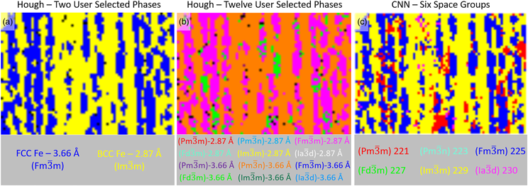
Figure 2 highlights the need for a reliable tool to assist an operator with symmetry determination using a section of 2205 duplex steel. In the case where the phases are known in advance (Fig. 2a), Hough-based EBSD is shown to produce a high-fidelity phase map of the austenite islands (blue) in the ferrite matrix (yellow). However, in cases where the phases are unknown, there exists ample opportunity for misclassification in the Hough-based method even when using what could be considered ideal acquisition parameters. If the six space groups used in the CNN study were selected in duplicate, one copy with lattice parameters matching the austenite's lattice parameters and symmetry and the other copy matching the ferrite's, the results can be strikingly different (Fig. 2b). In fact, not a single pattern is indexed to either of the two correct phases. Furthermore, two of the three space groups selected,  $Pm\bar{3}n$ (orange) and $Fd\bar{3}m$ (lime green), are not present in the sample. Thus, a robust classifier of EBSD patterns would be a useful tool for assisting with selecting the proper phases or alerting users to potential errors in selected phase lists. Figure 2c demonstrates how a CNN-based classifier could be used for such a purpose. The CNN has predicted the space group of each high-quality EBSP that Hough-based EBSD used for generating Figures 2a and 2b, yet the CNN-derived phase map is a much higher fidelity mapping of Figure 2a than Figure 2b, albeit without the lattice parameter information at this stage of the CNN model. These results are significant since Figure 2b demonstrates a marked failure wherein Hough-based EBSD cannot distinguish between the two correct answers plus ten phases with the same lattice parameters but different space group symmetry. Given the potential the CNN-based method has for improving the EBSD process, this work sets out to study how reliable the CNN's classifications are as new data captured under different diffraction conditions is presented to it.

Fig. 2. Hough-based EBSD results with different phase lists. A comparison of the Hough-based EBSD method is performed where (a) only the two correct phases are provided as options and (b) 12 options are made available based on the six space groups used in this work and the two lattice parameters found in the duplex steel sample. The CNN-derived space group map (c) details the classifier's predictions for the same EBSD patterns used in parts (a) and (b). The data for each map are collected using the ideal parameters defined as “default” in this work. It is worth noting that the CNN-derived map is derived from having the solution for each EBSP classified from among the six cubic space groups in the trained model.
Effects on the EBSD Patterns
It is important to understand the effect of varying the operating conditions of the SEM and EBSD detector on the electron diffraction patterns. Figure 3 visually details the effects by displaying the same diffraction pattern observed under different operating conditions. The larger versions of these images are contained in Figures A.1–A.5. Increasing the number of frames averaged for each diffraction pattern increases the signal-to-noise ratio and results in better resolution of finer details in the diffraction patterns. Changing the detector tilt changes the relative position of the image with respect to the interaction volume of the sample, referred to as the pattern center in EBSD (Schwartz et al., Reference Schwartz, Kumar, Adams and Field2009; Basinger et al., Reference Basinger, Fullwood, Kacher and Adams2011; Zhu et al., Reference Zhu, Kaufmann and Vecchio2019). For tilt angles that are far from the ideal conditions, the top or bottom edge of the EBSP may display blurring. The most significant blurring is observed when using a tilt of 13.3°. Otherwise, the changes are observed to be limited to small differences in the region of the Kikuchi sphere captured. Decreasing the sample-to-detector distance, and thus moving closer to the sample, results in the capture of significantly more solid angle. Since the EBSD detector is capturing a gnomonic projection, the increase in the solid angle means a greater area of the Kikuchi sphere is observed. This likely must be balanced with the ability to resolve the finer details and eventual blurring of the pattern edges. On the other hand, moving the detector further away captures less of the Kikuchi sphere but “magnifies” the finer details. The diffraction elements also appear slightly blurred at the furthest distance away from the sample. Changes to the SEM accelerating voltage affect the EBSPs by altering the wavelength of the incoming electrons. A decrease in the accelerating voltage increases the electron wavelength and therefore causes the Kikuchi bands to appear wider and vice versa. This results in more diffraction information from the same region of the Kikuchi sphere condensed within the viewing window for higher accelerating voltages. Note that it does not have the same effect as changing the detector distance. Lastly, the Oxford Symmetry detector can capture patterns at one of three resolutions: 156 × 128, 622 × 512, or 1,244 × 1,024. These are described as low, medium, and high resolution, respectively, in this work. For each of the different imaging conditions shown, approximately 3,000 diffraction patterns are collected from the same region of each sample and the CNNs performance analyzed.

Fig. 3. Impact of operating conditions on the EBSD patterns. The diffraction pattern for a point on the sample is displayed for different imaging conditions. The effect of the number of frames averaged, the tilt of the EBSD detector, the sample-to-detector distance for the EBSD detector, the SEM accelerating voltage, and the resolution at which patterns are captured are each visually described.
Frame Averaging
Figure 4 presents a visual overview of the pattern classification results for each frame averaging condition studied using a sample of 2205 duplex stainless steel, a material with a ferrite matrix (space group 229; yellow) and austenite islands (space group 225; blue) (Momeni et al., Reference Momeni, Dehghani and Zhang2012). Similar space group maps for each of the parameters studied are shown in the Appendix (Figs. A.6–A.10). The electron image (Fig. 4a) and Hough-based phase map (Fig. 4b) are provided as the ground truth, since these phases can be differentiated by Hough with relative ease, assuming that the operator selects the correct phases at the start (i.e., user knows the phases). Without any frame averaging, the EBSPs are lacking much of the available details and essentially all the EBSPs from this sample are misidentified (Fig. 4c). Increasing the frame averaging to five improves the result (Fig. 4d), but it is not until ten frames are averaged that a reasonable number of classifications appear to be correct (Fig. 4e) when compared with the Hough-based map (Fig. 4b). Figures 4f and 4g each show sequential improvements over Figure 4e as nearly all of the patterns become correctly classified to the correct space group (i.e., matching the Hough-based phase map). As seen in the plot (Fig. 4h), the number of patterns classified to each space group begins to improve with ten frames averaged. While the plot shows the relative number of patterns classified to each space group compared with Hough-based EBSD, the space group maps made from the CNN's predictions establish whether the individual EBSPs are correctly classified based on their correlation with the Hough-based phase map. Since each of the other materials studied in this work is known to be single-phase, normalized classification accuracy precisely describes the model performance.

Fig. 4. Visual overview of frame averaging on CNN classification for duplex steel. (a) Electron image of the region of dual-phase 2205 duplex steel. (b) Hough-based EBSD phase map of the fcc (225) austenite (blue) and bcc (229) ferrite (yellow). (c) Phase map generated from EBSD patterns collected with no frame averaging applied (i.e., one frame). (d) Phase map generated from EBSD patterns collected with five frame averaging applied. (e) Phase map generated from EBSD patterns collected with ten frame averaging applied. (f) Phase map generated from EBSD patterns collected with 20 frame averaging applied. (g) Phase map generated from EBSD patterns collected with 30 frame averaging applied. (h) Plot showing the fraction of patterns indexed to each space group as a function of frame averaging. Thirty frame averaging is the default parameter and is designated as such by the blue star for space group 225 and a yellow star for space group 229. Trend lines are fit with a third order polynomial. Scale bar = 25 μm. There are 3,848 diffraction patterns (pixels) in each phase map.
It is worth pointing out that the Hough-based result is considered the ground truth (or correct answer) because the phases in the sample are known, and the known answer is provided as input to the Hough-based solution. So in this context, the EBSD solution for phase ID must already be known for the Hough-based approach. The power of the machine learning approach being implemented here, and previously presented in Kaufmann et al. (Reference Kaufmann, Zhu, Rosengarten and Vecchio2020d), is to perform symmetry identification, to the space group level, for samples for which the phases present are not known a priori (i.e., enable true phase ID by EBSD).
Figure 5 details the normalized accuracy of the CNN for each space group as the number of frames averaged is varied in subsequent collections of the same EBSPs. The default frame averaging is 30 patterns. It is observed that a high overall classification accuracy, compared with the accuracy obtained for the default parameter, is generally retained as low as 5–10 frames averaged. An exception to this is observed for space groups 221 and 229 which, along with space group 225, are the most difficult for the CNN to differentiate owing to the strong similarities between the fcc and L12 structures and bcc and B2 structures used in training the model (Kaufmann et al., Reference Kaufmann, Zhu, Rosengarten and Vecchio2020d).

Fig. 5. Effect of frame averaging on classification accuracy. The normalized classification accuracy of the trained CNN for each space group based on the number of patterns averaged during data collection. The space groups are (a)  $Pm\bar{3}m$, (b) $Pm\bar{3}n$, (c) $Fm\bar{3}m$, (d) $Pd\bar{3}m$, (e) $Im\bar{3}m$, and (f) $Ia\bar{3}d$. The default number of frames averaged is 30.
Detector Tilt
Figure 6 details the effect of the detector tilt on the CNN's classification of the collected EBSPs. Note that the detector tilt is reported as the angle of the detector arm above horizontal. Referring to the EBSPs in Figure 3 and their enlarged counterparts shown in Figure A.2, detector tilts of 14.2–13.7° show ideal patterns with little or no blurring at the edges. The blurring becomes more apparent at the bottom of the EBSPs when a tilt of 13.5° is applied and increases in severity at a tilt of 13.3°. For most space groups in Figure 6, the model is found to be highly resilient, and it is only at or below a tilt of 13.5° that any notable changes in accuracy occur. Again, space groups 221 and 229 are the exception to this observation. Referring to the symmetry maps of the duplex steel, the fractions do not vary significantly across the individual maps (Fig. A.7) and the space group classification of each EBSP aligns well with the Hough-based phase map (ground truth).

Fig. 6. Effect of detector tilt on classification accuracy. The normalized classification accuracy of the trained CNN for each space group based on the tilt of the detector during data collection. The space groups are (a)  $Pm\bar{3}m$, (b) $Pm\bar{3}n$, (c) $Fm\bar{3}m$, (d) $Pd\bar{3}m$, (e) $Im\bar{3}m$, and (f) $Ia\bar{3}d$. The detector tilts are reported as the detector arm angle above horizontal. The default value for detector tilt is 13.7°.
Detector Distance
Figure 7 presents the changes in the CNN's performance as the EBSD detector collects the diffraction patterns at different sample-to-detector distances. The number of misclassified pixels, however minute the difference is, is observed to scale with an increased absolute distance from the default condition of 19.1 mm. When the detector is much further away from the sample, less solid angle is captured, and the diffraction patterns become distorted (Fig. 3 and Fig. A.3). Moving closer to the sample increases the solid angle, but at the expense of the finer details. This likely contributes to the noticeably reduced performance for the closest possible setting (a sample-to-detector distance of 14.3 mm). Referring to the phase maps of the duplex steel (Fig. A.8), similar effects are observed. As the sample-to-detector distance gets further from the default condition, the CNN-derived maps increasingly differ from the Hough-based phase map.

Fig. 7. Effect of sample-to-detector distance on classification accuracy. The normalized classification accuracy of the trained CNN for each space group based on the sample-to-detector distance during data collection. The space groups are (a)  $Pm\bar{3}m$, (b) $Pm\bar{3}n$, (c) $Fm\bar{3}m$, (d) $Pd\bar{3}m$, (e) $Im\bar{3}m$, and (f) $Ia\bar{3}d$. The default value for sample-to-detector distance is 19.1 mm.
Accelerating Voltage
The effect of changing the wavelength of the incoming electrons by modifying the accelerating voltage is explored in Figure 8 and Figure A.9. The primary effect of changing the wavelength of the incoming electrons is a change in the width of the observed Kikuchi bands (Fig. 3 and Fig. A.4). The resulting effect on the collected diffraction patterns is similar to changing the detector distance, but notably does not alter the amount of solid angle captured on the phosphor screen. Instead, changing the accelerating voltage effectively changes the magnification of the diffraction data within the same screen area. For example, decreasing to 10 kV causes the details of the diffraction pattern to increase in size, effectively making the data appear expanded. Note how the same zone axes are present for each accelerating voltage, but the distance between the zone axes and the width of the diffraction lines appears to change (Fig. A.4). These changes are observed to have appreciable effects on the classification performance of the CNN. At 10 kV, many of the patterns from each space group are misclassified (Fig. 8). On the other hand, increasing to 30 kV accelerating voltage yields reasonably good classification performance, perhaps because the Kikuchi bands are narrower and more information appears to be visible. The same effects on performance are visually evident in the CNN-derived space group maps of the duplex steel (Fig. A.9).

Fig. 8. Effect of accelerating voltage on CNN classification. The normalized classification accuracy of the trained CNN for each space group based on the SEM accelerating voltage. The space groups are (a)  $Pm\bar{3}m$, (b) $Pm\bar{3}n$, (c) $Fm\bar{3}m$, (d) $Pd\bar{3}m$, (e) $Im\bar{3}m$, and (f) $Ia\bar{3}d$. An accelerating voltage of 20 kV is the default.
Pattern Resolution
Reducing the initial resolution of the collected diffraction patterns bins the information from neighboring pixels to accelerate the rate of collection. Figure 9 details the CNN's performance after collecting the diffraction patterns at each of the three available resolutions for the Oxford Symmetry EBSD detector. The CNN is capable of achieving a high degree of accuracy even when patterns are collected at the lowest resolution setting. Only space groups 221 and 229 are appreciably impacted owing to the strong similarities between the fcc and L12 structures and bcc and B2 structures used in training the CNN. Figure A.10 visually demonstrates the reliable performance of the CNN at each pattern resolution by creating structure maps for the 2205 duplex steel.

Fig. 9. Effect of pattern resolution on CNN classification. The normalized classification accuracy of the trained CNN for each space group based on the EBSD detector resolution. Available resolutions are 156 × 128 (low), 622 × 512 (medium), and 1,244 × 1,024 (high). The space groups are (a)  $Pm\bar{3}m$, (b) $Pm\bar{3}n$, (c) $Fm\bar{3}m$, (d) $Pd\bar{3}m$, (e) $Im\bar{3}m$, and (f) $Ia\bar{3}d$. High resolution (1,244 × 1,024) is the default setting.
Discussion
The electron diffraction community has recently begun to consider artificial intelligence a necessary component of next-generation microscopy (Spurgeon et al., Reference Spurgeon, Ophus, Jones, Petford-Long, Kalinin, Olszta, Dunin-Borkowski, Salmon, Hattar, Yang, Sharma, Du, Chiaramonti, Zheng, Buck, Kovarik, Penn, Li, Zhang, Murayama and Taheri2020). Much of this is driven by the rate at which modern microscopes can generate high-quality data (Goulden et al., Reference Goulden, Trimby and Bewick2018); as a result, human knowledge and experience will no longer be an efficient means of analysis. If AI-based tools are to be implemented effectively, it is necessary for the community to identify potential areas of fragility, for example, changing diffraction conditions, and assess the impact in order to further development and increase trust in these “black-box” models.
EBSD was selected as an ideal technique owing to the ease of varying each parameter and the rates of data collection achievable (Schwartz et al., Reference Schwartz, Kumar, Adams and Field2009; Goulden et al., Reference Goulden, Trimby and Bewick2018). Furthermore, several recent studies have explored the use of CNNs applied to components of EBSD analysis (Jha et al., Reference Jha, Singh, Al-Bahrani, Liao, Choudhary, De Graef and Agrawal2018; Shen et al., Reference Shen, Pokharel, Nizolek, Kumar and Lookman2019; Ding et al., Reference Ding, Pascal and De Graef2020; Kaufmann et al., Reference Kaufmann, Maryanovsky, Mellor, Zhu, Rosengarten, Harrington, Oses, Toher, Curtarolo and Vecchio2020a, Reference Kaufmann, Zhu, Rosengarten, Maryanovsky, Harrington, Marin and Vecchio2020b); however, these efforts have thus far only been tested with new data collected or simulated using identical geometry and diffraction conditions. Herein, a parametric analysis of five parameters commonly found among electron diffraction techniques was performed to examine the performance of a CNN trained to classify diffraction patterns. One material was selected per space group and new diffraction patterns were collected starting with diffraction conditions matching the training set and then the same patterns were recollected 16 more times after setting just one parameter to a value different from the default conditions. The same analysis was performed for a sample of 2205 duplex steel to demonstrate CNN-based symmetry mapping (Kaufmann et al., Reference Kaufmann, Zhu, Rosengarten, Maryanovsky, Wang and Vecchio2020c) a sample with each varied parameter. If the trained CNN is highly sensitive to the diffraction conditions, we would have expected to see large decreases in performance with the smallest changes. For example, by changing the sample-to-detector distance, the Kikuchi bands from the same material can appear wider or narrower and the distance between diffraction information (e.g., zone axes) appears to change. However, the CNN's classification accuracy is observed to be quite stable (i.e., small reductions in classification accuracy) in comparison to the results achieved with the default conditions, suggesting that the features detectors learned by the model are not biased to these characteristics. This was one of the intended goals of using multiple materials with different z-contrast and lattice parameters for the same space group in the training set (Kaufmann et al., Reference Kaufmann, Zhu, Rosengarten and Vecchio2020d), and this study indicates its effectiveness. Moreover, the CNN is also observed to be highly dependable after decreasing the signal-to-noise ratio of the captured diffraction pattern by reducing the frame averaging. Decreasing the number of frames averaged will allow for faster data collection, as much as six times faster if averaging 5 frames compared to 30, while maintaining a high degree of classification accuracy for most materials. In each of the studies within this work, the space groups most likely to be misclassified by the model were 221  $( {Pm\bar{3}m\;} )$ and 229 $( {Im\bar{3}m\;} )$. As previously mentioned, the misclassification of these patterns can be at least partially attributed to the strong similarities between diffraction patterns from the fcc $( {Fm\bar{3}m} )$ and L12 $( {Pm\bar{3}m} )$ structures and bcc $( {Im\bar{3}m} )$ and B2 $( {Pm\bar{3}m} )$ structures used in training the CNN (Kaufmann et al., Reference Kaufmann, Zhu, Rosengarten and Vecchio2020d). Inclusion of more diverse data for these space groups may help alleviate this concern in addition to being a practical advancement toward commercial adoption. While the model's dependability and trustworthiness with respect to equipment parameters has now been evaluated for phase differentiation and identification problems, it is still important to test this hypothesis for EBSD orientation indexing CNNs (Jha et al., Reference Jha, Singh, Al-Bahrani, Liao, Choudhary, De Graef and Agrawal2018; Shen et al., Reference Shen, Pokharel, Nizolek, Kumar and Lookman2019; Ding et al., Reference Ding, Pascal and De Graef2020). A much larger study should also be performed to investigate the effects of co-varying operating parameters; however, we expect that similar tolerances will be observed based on the reliability observed under diffraction conditions far from the training data. This expectation stems from the observation that changing individual parameters can cause drastic changes to the patterns and the CNN generally maintains exceptional performance.
Conclusions
In this work, a systematic study of the EBSD operating parameters and their individual effects on the classification performance of a CNN is performed. Despite the CNN being trained from diffraction patterns captured with a fixed geometry and SEM settings, it is found to be resilient over a wide range of conditions. Markedly decreased performance is generally only observed for the most challenging materials to differentiate (e.g., B2 and bcc or L12 and fcc). Furthermore, it is encouraging to verify that parameters that effect the time to map an area (e.g., frame averaging or pattern resolution) can be modified to accelerate the process without substantially degrading model performance. For parameters such as tilt, it is reassuring to validate the model performs well over a variety of reasonable parameters. Although the CNN may not achieve high accuracy under all conditions, such as a low number of frames averaged, when used appropriately it remains a highly capable method for assisting the user with phase identification and provides a level of phase differentiation markedly above what state-of-the-art commercial methods are currently capable of. In the current version of the CNN, the parameter settings that cause noteworthy reductions in performance across a majority of space groups are a frame averaging of 1 or utilizing 10 kV accelerating voltage. In the future, training models with patterns collected using a wider variety of operating conditions, particularly those with the largest effect on performance, could result in a model that is even more resilient to some of these types of perturbations to the diffraction patterns; although it may still not be possible to overcome all limitations, such as no frame averaging, owing to significant reductions in the signal-to-noise ratio. A future study should also investigate the co-variation of parameters from the default conditions. Ultimately, we expect the results of this research to encourage the continued development of these tools given the reliability observed and their potential to assist with or automate the analysis of electron diffraction patterns.
Availability of Data and Materials
The datasets generated during and/or analyzed during the current study are available from the corresponding author on reasonable request. The code for implementing the deep neural network is available through Zenodo (doi: 10.5281/zenodo.3564937) (krkaufma, 2019).
Acknowledgments
K.K. was supported by the Department of Defense (DoD) through the National Defense Science and Engineering Graduate Fellowship (NDSEG) Program. K.K. would also like to acknowledge the support of the ARCS Foundation, San Diego Chapter. K.S.V. would like to acknowledge the financial generosity of the Oerlikon Group in support of his research group.
Conflict of interest
The authors declare no competing interests.
Appendix
See Figs. A.1–A.10 and Table A.1

Fig. A.1. Diffraction pattern with increasing frame averaging. A visual explanation of the observed changes based on the number of frames averaged during the capture of each diffraction pattern.

Fig. A.2. Diffraction pattern with different detector tilt. A visual explanation of the observed changes based on the tilt of the EBSD detector above the horizontal.

Fig. A.3. Diffraction pattern with decreasing sample-to-detector distance. A visual explanation of the observed changes based on the proximity of the EBSD detector to the sample. Larger detector distances are further from the sample.

Fig. A.4. Diffraction pattern with variable accelerating voltage. A visual explanation of the observed changes based on the accelerating voltage applied to the incoming electrons.

Fig. A.5. Diffraction pattern with variable detector resolution. A visual explanation of the observed changes based on the resolution of the EBSD detector.

Fig. A.6. Visual overview of frame averaging on CNN classification for duplex steel. (a) Electron image of the region of dual-phase 2205 duplex steel. (b) Hough-based EBSD phase map of the fcc (225) austenite (blue) and bcc (229) ferrite (yellow). (c) Phase map generated from EBSD patterns collected with no frame averaging applied (i.e., one frame). (d) Phase map generated from EBSD patterns collected with five frame averaging applied. (e) Phase map generated from EBSD patterns collected with ten frame averaging applied. (f) Phase map generated from EBSD patterns collected with 20 frame averaging applied. (g) Phase map generated from EBSD patterns collected with 30 frame averaging applied. (h) Plot showing the fraction of patterns indexed to each space group as a function of frame averaging. Thirty frame averaging is the default parameter and is designated as such by the blue star for space group 225 and a yellow star for space group 229. Trend lines are fit with a third-order polynomial. Scale bar = 25 μm. There are 3,848 diffraction patterns (pixels) in each phase map.

Fig. A.7. Visual overview of detector tilt on CNN classification for duplex steel. (a) Phase map generated from EBSD patterns collected with a detector tilt of 14.2°. (b) Phase map generated from EBSD patterns collected with a detector tilt of 14.0°. (c) Phase map generated from EBSD patterns collected with a detector tilt of 13.7°. (d) Phase map generated from EBSD patterns collected with a detector tilt of 13.5°. (e) Phase map generated from EBSD patterns collected with a detector tilt of 13.3°. (f) Plot showing the fraction of patterns indexed to each space group as a function of detector tilt. A detector tilt of 13.7° above horizontal is the default parameter and is designated as such by the blue star for space group 225 and a yellow star for space group 229. Trend lines are fit with a third-order polynomial. There are 3,848 diffraction patterns (pixels) in each phase map.

Fig. A.8. Visual overview of detector distance on CNN classification for duplex steel. (a) Phase map generated from EBSD patterns collected with a sample-to-detector distance of 24.3 mm. (b) Phase map generated from EBSD patterns collected with a detector distance of 21.8 mm. (c) Phase map generated from EBSD patterns collected with a detector distance of 19.1 mm. (d) Phase map generated from EBSD patterns collected with a detector distance of 16.8 mm. (e) Phase map generated from EBSD patterns collected with a detector distance of 14.3 mm. (f) Plot showing the fraction of patterns indexed to each space group as a function of sample-to-detector distance. A detector distance of 19.1 mm is the default parameter and is designated as such by the blue star for space group 225 and a yellow star for space group 229. Trend lines are fit with a third-order polynomial. There are 3,848 diffraction patterns (pixels) in each phase map.

Fig. A.9. Visual overview of accelerating voltage on CNN classification for duplex steel. (a) Phase map generated from EBSD patterns collected with an electron accelerating voltage of 10 kV. (b) Phase map generated from EBSD patterns collected with an electron accelerating voltage of 20 kV. (c) Phase map generated from EBSD patterns collected with an electron accelerating voltage of 30 kV. (d) Plot showing the fraction of patterns indexed to each space group as a function of accelerating voltage. An electron accelerating voltage of 20 kV is the default parameter and is designated as such by the blue star for space group 225 and a yellow star for space group 229. Trend lines are fit with a third-order polynomial. There are 3,848 diffraction patterns (pixels) in each phase map.

Fig. A.10. Visual overview of pattern resolution on CNN classification for duplex steel. (a) Phase map generated from EBSD patterns collected with a detector resolution of 156 × 128 (low). (b) Phase map generated from EBSD patterns collected with a detector resolution of 622 × 512 (medium). (c) Phase map generated from EBSD patterns collected with a detector resolution of 1,244 × 1,024 (high). (d) Plot showing the fraction of patterns indexed to each space group as a function of EBSD pattern resolution. The default pattern resolution is 1,244 × 1,024 and is designated as such by the blue star for space group 225 and a yellow star for space group 229. Trend lines are fit with a third-order polynomial. There are 3,848 diffraction patterns (pixels) in each phase map.
Table A.1. Pattern Acquisition Rates.


 Open access