Hostname: page-component-848d4c4894-xm8r8 Total loading time: 0 Render date: 2024-06-30T22:08:37.412Z Has data issue: false hasContentIssue false

2D Junction Profiling on Semiconductor Device Reliability Fail

Published online by Cambridge University Press:  04 August 2017

Y.Y. Wang
Affiliation:
Globalfoundires Inc. Hudson Valley Research Park, 2070 Route 52, Hopewell Jct., NY, USA
J. Nxumalo
Affiliation:
Globalfoundires Inc. Hudson Valley Research Park, 2070 Route 52, Hopewell Jct., NY, USA
A. Katnani
Affiliation:
Globalfoundires Inc. Hudson Valley Research Park, 2070 Route 52, Hopewell Jct., NY, USA
D. Ioannou
Affiliation:
Globalfoundires Inc. Hudson Valley Research Park, 2070 Route 52, Hopewell Jct., NY, USA
J. Brown
Affiliation:
Globalfoundires Inc. Hudson Valley Research Park, 2070 Route 52, Hopewell Jct., NY, USA
K. Bandy
Affiliation:
Globalfoundires Inc. Hudson Valley Research Park, 2070 Route 52, Hopewell Jct., NY, USA
M. Macdonald
Affiliation:
Globalfoundires Inc. Hudson Valley Research Park, 2070 Route 52, Hopewell Jct., NY, USA
J. Bruley
Affiliation:
IBM T. J. Watson Research Center, 1101 Kitchawan Road, Route 134, Yorktown Heights, NY, USA

Abstract

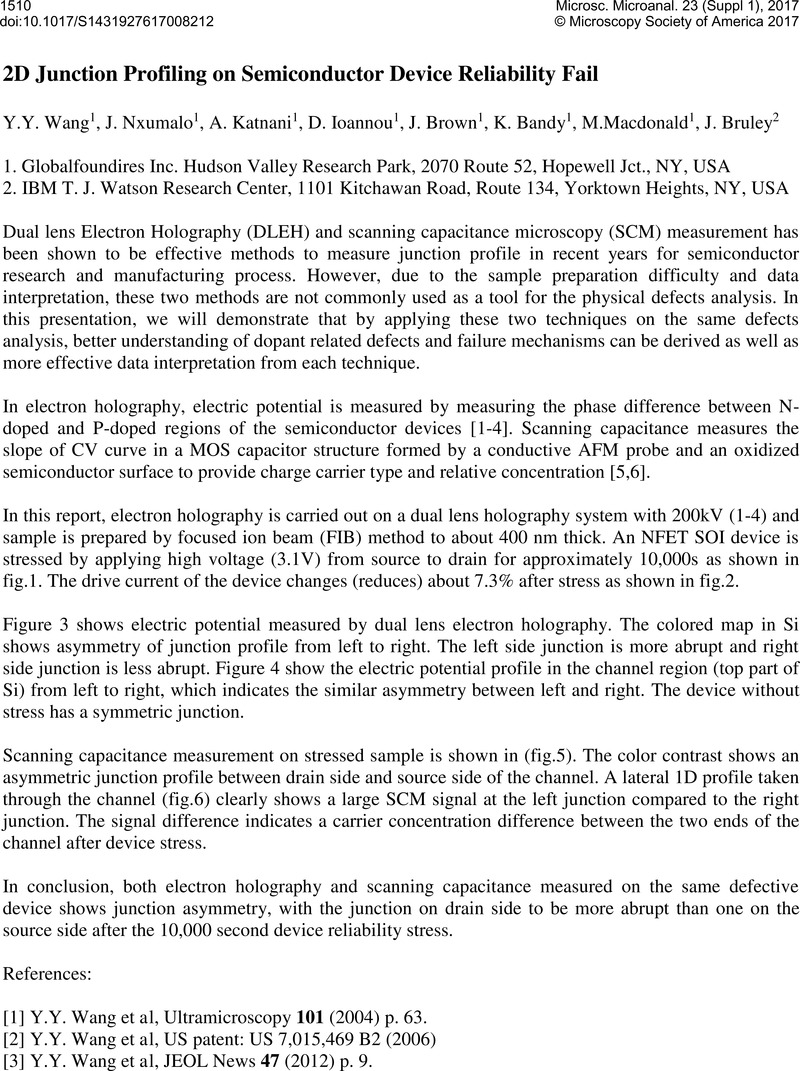
Image of the first page of this content. For PDF version, please use the ‘Save PDF’ preceeding this image.'
Type
Abstract
Copyright
© Microscopy Society of America 2017 

References

[1] Wang, Y.Y., etal, Ultramicroscopy 101 2004). p. 63.Google Scholar
[2] Wang, Y.Y., et al, US patent: US 7,015,469 B2 (2006).Google Scholar
[3] Wang, Y.Y., et al, JEOL News 47 2012). p. 9.Google Scholar
[4] Wang, Y.Y., et al, Ultramicroscopy 124 2013). p. 117.Google Scholar
[5] Williams, C. C., et al, J. Vac. Sci. Technol. A 8 1990). p. 895.CrossRefGoogle Scholar
[6] Yuan Tour, Semiconductor device Physics.Google Scholar