


Introduction
The family of III-V nitrides (GaN, InGaN, AlGaN) has recently attracted much attention because of their wide spectrum of potential applications ranging from opto-electronic devices for the blue-ultraviolet spectral region to high temperature devices [Reference Nakamura, Senoh, Nagahama, Iwasa, Yamada, Matsushita, Kiyoku, Sugimoto, Kozaki, Umemoto, Sano and Chocho1,Reference Song, Kuball, Nurmikko, Bulman, Doverspike, Shappard, Weeks, Leonard, Kong, Dieringer and Edmonds2]. High-temperature processing of nitrides is an essential part of the nitride device fabrication, i.e., for the activation of Mg-acceptors to achieve p-doping of GaN or for the fabrication of ohmic contacts [Reference Nakamura, Mukai, Senoh and Iwasa3,Reference Khan, Chen, Skogman and Kuznia4]. Monitoring the thermal stability of GaN during high-temperature annealing is therefore of great interest [Reference Kuball, Demangeot, Frandon, Renucci, Massies, Grandjean, Aulombard and Briot5-Reference Hong, Lee, MacKenzie, Donovan, Abernathy, Pearton and Zolper7]. Since changes in the near-surface stoichiometry that deteriorate electrical properties occur at a temperature, which is about 100°C lower than the temperature where visible surface degradation occurs, it is essential to develop effective non-invasive ex-situ as well as in-situ monitoring techniques to assess changes in the quality of GaN and AlGaN layers at elevated temperatures. So far only time-consuming techniques like atomic force microscopy (AFM) and transmission electron microscopy (TEM) have been used to assess degradation effects [Reference Zolper, Crawford, Howard, Ramer and Hersee6,Reference Hong, Lee, MacKenzie, Donovan, Abernathy, Pearton and Zolper7].
In this report, we illustrate the potential applications of Raman scattering (complemented by photoluminescence experiments) to determine and monitor the degradation pathway of GaN during high-temperature annealing. The results of this study can be employed for the non-invasive optical monitoring of structural damage to GaN during high-temperature processing as well as for the non-invasive optical monitoring of passive and active nitride devices operating at elevated temperatures. Raman scattering provides information on vibrational states of GaN, which are sensitive to microscopic disorder. The crystalline quality can be judged from the peak shapes and the selection rules. GaN normally crystallize in the hexagonal wurtzite structure (space group C6v 4) with four atoms in the unit cell. At k=0 group theory predicts the following eight sets of phonon modes: 2A1 + 2B1 + 2E1+ 2E2 of which only one A1, one E1 and two E2 are Raman active. One set of A1 and one set of E1 corresponds to acoustic phonons, the B1 modes are silent [Reference Siegle, Kaczmarczyk, Filippidis, Litvinchuk, Hoffmann and Thomsen8]. The activation of q ≠ 0 phonons of GaN by disorder allows us to probe and assess noninvasively changes in the crystalline quality of GaN. We find clear indications for a interfacial reaction between sapphire and GaN at elevated temperatures.
Experiment
Raman scattering and photoluminescence spectra were recorded from high-temperature annealed GaN layers. The samples were annealed in nitrogen ambient in a heating stage at temperatures from 100°C to 1100°C in 50−100°C steps, in a sequence of 20min anneals. A small amount of oxygen was present during the annealing. Raman spectra were collected after each annealing step on a Renishaw Raman microscope system 2000 using the 488nm line of an Ar+-laser as excitation source. Photoluminescence spectra were recorded using a Renishaw ultraviolet (UV) Raman microscope system with the 244nm line of an intra-cavity frequency doubled Ar+ laser as excitation source. The Raman measurements were performed in backscattering Z(Y,Y)□geometry, however, when necessary a full polarization analysis was performed. The studied GaN samples, 2 μm thick, were grown by molecular-beam epitaxy (MBE) and metalorganic vapor phase epitaxy (MOCVD) at growth temperatures of 980-1150°C on sapphire [0001] substrates, after a thin buffer layer of low temperature GaN had been deposited at 550-600°C. The MBE sample was doped with Mg, annealed in nitrogen ambient at 750°C for 30 min, with a free carrier concentration of about 3×1017cm−3 and a mobility of 8cm2/Vs. The MOCVD sample was unintentionally n-doped.
Results
Raman scattering
Figure 1 shows Raman spectra of the MBE-grown GaN layer after various 20min anneals, recorded at room temperature in backscattering ZY,Y)Z geometry. The Raman spectrum shows before annealing (lowest spectrum) the allowed E2(high) phonon at 567 cm−1 and the A1(LO) phonon at 734 cm−1. We observe at 534cm−1 the A1(TO) mode which is usually not allowed in this configuration, however, might be related to a high defect density or the p-doping. The mode at 750 cm−1 is a reminiscent of the Eg sapphire mode. The shown spectra are normalized to the E2 phonon intensity.
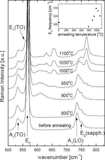
Figure 1: Raman spectra of the MBE-grown GaN sample after 20min anneals at various temperatures, recorded at room temperature in backscattering Z(Y,Y)Z geometry.
The Raman spectrum of the MBE-grown GaN layer remains unchanged for annealing temperatures up to 800−900°C. Heat treatments at temperatures between 900°C to 1000°C, however, result in a broad Raman peak, centered at 610cm−1, between the E2 and A1(LO) phonon lines. A polarization analysis reveals that this new feature in the Raman spectrum is present in parallel and in crossed polarizations [Z(Y,Y)Z, Z(X,Y)Z]. The E2 phonon shifts from 567cm−1 before annealing to 570cm−1 after annealing at 1000°C (inset of Fig. 1), whereas the A1(LO) phonons remains unaffected within the experimental spectral resolution.
Annealing the sample at a temperature higher than 1000°C results in distinct Raman peaks at 630cm−1, 656cm−1 and 770cm−1. Their intensity increases in the subsequent annealing steps. The A1(LO) phonon at 734cm−1 broadens and decreases in intensity. The E1(TO) phonon emerges at 559cm−1 on the low-energy side of the E2 phonon (uppermost spectrum in Figure 1). We observe a tentative decrease in the E2 phonon frequency for the 1100°C anneal (inset of Fig.1).
The Raman features induced by the 1000°C and 1100°C anneal are present in all polarization configurations with no evident polarization dependence. We note that the magnitude of the broad Raman peak at 610cm−1 after annealing at 1100°C is sample-to-sample dependent: it apparently decreases in Figure 1, whereas for other samples a further increase was observed during the high-temperature annealing. The dramatic changes in the Raman spectrum for anneals higher than 1000°C go along with modifications in the surface morphology. We observe a pitting of the surface, however, the surface remains visually mirror-like. Macroscopic disorder appears.
Additional Raman experiments were performed on the MOCVD-grown GaN sample. The observed characteristic changes in the Raman spectrum during the annealing sequence are similar to the results shown in Figure 1. The temperature regimes, however, appear to be somewhat different for the MBE- and MOCVD-grown sample. Figure 2 compares Raman spectra obtained from the MOCVD- and MBE-grown GaN sample (comparable layer thickness) in the spectral region of the A1(LO) phonon, after annealing the sample at a temperature of 1050°C. The emerging distinct Raman peaks at 630cm−1, 656cm−1 and 770cm−1, illustrating the severe degradation of the sample, seem to be less pronounced for the MOCVD-grown GaN layer. The investigated MOCVD-grown GaN layer appears therefore to be thermally more stable than the investigated MBE-grown GaN layer.

Figure 2: Raman spectra of MBE-grown GaN and MOCVD-grown GaN annealed at 1050°C.
Photoluminescence
Figure 3 and 4 show photoluminescence spectra of the MBE-grown GaN sample recorded in the spectral region of the well-known R-lines of sapphire and the GaN bandgap, respectively, after the various high-temperature anneals. Annealing at a temperature of 1000°C and 1100°C results in a strong photoluminescence signal around 1.75eV. Furthermore, we detect a shift and broadening of the sapphire R-lines. Figure 4 shows the photoluminescence spectrum of the MBE-grown GaN sample in the spectral region of the GaN bandgap. Before annealing we detect photoluminescence from the GaN bandgap at 3.4eV. Annealing at high temperature results in a decreasing bandgap photoluminescence intensity, a broadening of the photoluminescence signal, as well as a shift of the photoluminescence maximum towards higher photon energies.

Figure 3: Photoluminescence spectrum of the MBE-grown GaN sample, after various 20min anneals.

Figure 4: Photoluminescence spectrum of the MBE-grown GaN sample, after various 20min anneals.
Discussion
The evolution of the GaN Raman spectrum shown in Figure 1 allows us to determine and monitor noninvasively the degradation pathway of GaN during the annealing sequence. Three thermal stability/degradation regimes can be identified: (1) annealing temperatures up to 800−900°C, (2) between 900° and 1000°C and (3) higher than 1000°C. Below 900°C no structural degradation of the GaN is evident from the Raman spectra. This is consistent with previous reports [Reference Hong, Lee, MacKenzie, Donovan, Abernathy, Pearton and Zolper7,Reference Siegle, Kaczmarczyk, Filippidis, Litvinchuk, Hoffmann and Thomsen8]. Such temperatures are well suited for high-temperature processing as well as active and passive high-temperature devices. Annealing temperatures higher than 900°C result in the degradation of the crystalline quality of the GaN layer, which is evident in the emerging broad Raman peak between the E2 and A1(LO) phonon (Figure 1). Microscopic defects created by the high-temperature annealing result in the breakdown of the translational symmetry and the activation of the phonon density of states in the Raman spectrum, i.e., the participation of q ≠ 0 phonons in the Raman scattering process (disorder-induced Raman scattering). The broad Raman peak at 610cm−1 is located in a spectral region with a high phonon density of states according to lattice dynamical calculations by Azuhata et al. [Reference Azuhata, Matsunaga, Shimada, Yoshida, Sota, Suzuki and Nakamura9]. It is present in all polarization configurations as expected for disorder-induced Raman scattering. Consistently, we observe a decreasing band edge photoluminescence signal during the annealing sequence as shown in Figure 4. Similar changes in the GaN photoluminescence spectrum were reported by Lin et al. [Reference Lin, Sverdiov and Morkoç10] in low-temperature photoluminescence experiments on GaN samples, which were annealed at 900°C for 30min, i.e., pointing to non-radiative recombination centers. Note that no obvious modifications in the surface morphology are visible after the annealing. The observed frequency shift of the E2 phonon by about 3cm−1 during the annealing sequence (inset of Figure 1) reflects the appearance of internal stress [Reference Demangeot, Frandon, Renucci, Briot, Gil and Aulombard11].
Forbidden sapphire modes were observed by Barker et al. [Reference Barker12] at 633cm−1, 652cm−1 and 770cm−1 on surface-damaged sapphire. The activation of the forbidden 770cm−1 sapphire mode for annealing temperatures higher than 1000°C (Figure 1) is therefore a clear indication for a degradation of the GaN/sapphire interface during the high-temperature annealing, i.e., a reaction between GaN and sapphire at the interface. No GaN modes or a high GaN phonon density of states is present around 770cm−1 and could contribute [Reference Azuhata, Matsunaga, Shimada, Yoshida, Sota, Suzuki and Nakamura9]. The observed photoluminescence signal at 1.75eV around the sapphire R-lines as well as the shift and broadening of the sapphire R-lines (Figure 4) consistently illustrate structural modifications at the GaN/sapphire interface (defects, stress) [Reference Grabner13]. We note that no change in the Raman or the photoluminescence spectrum of sapphire was observed when a plain sapphire wafer was annealed under the same conditions. The assignment of the 630cm−1 and 656cm−1 Raman modes in Figure 1 is more difficult since both sapphire with its forbidden modes at 633cm−1 and 652cm−1 as well as GaN [Reference Azuhata, Matsunaga, Shimada, Yoshida, Sota, Suzuki and Nakamura9] contribute in this frequency range. Raman experiments on the side face of an annealed 6μm–thick MBE-grown GaN layer, however, indicate that the 630cm−1 and 656cm−1 Raman modes mainly arise from the GaN/sapphire interface region suggesting a larger contribution from the forbidden sapphire modes. The presence of the E1(TO) phonon at 559cm−1 after the 1100°C anneal (Figure 1) shows an evolving misorientation of the GaN layer during the high-temperature annealing.
Conclusions
We have demonstrated the great potential of Raman scattering to detect damage in GaN induced by high-temperature annealing. The results can be applied to monitor noninvasively damage in GaN during high-temperature processing as well as to monitor passive and active high-temperature nitride devices. Three distinct regimes of thermal damage where identified by characteristic Raman spectra. Raman scattering reveals thermal damage due to microscopic defects for anneals between 900°C and 1000°C based on the appearance of a disorder-induced Raman scattering signal between the E2 and A1(LO) phonon. The evolving Raman spectrum displays the GaN phonon density of states. Above 1000°C, Raman scattering probes an interfacial reaction between GaN and sapphire, illustrated by the activation of forbidden sapphire modes. The investigated MOCVD-grown GaN sample was found to be thermally more stable than the investigated MBE-grown GaN sample. Defect-related photoluminescence was found after the high-temperature annealing of GaN. The E2 phonon frequency was analyzed to deduce information on internal stress. Annealing below 900°C has no effect on the GaN crystalline quality and is therefore well suitable for high-temperature applications of GaN.
Acknowledgments
We thank G.D. Pitt (Renishaw Transducers plc.) for financial support and supplying the heating stage, H. Sands and D.N. Batchelder (University of Leeds) for support for the ultraviolet photoluminescence experiments and B. Gil for helpful discussions and encouragement.


