Hostname: page-component-848d4c4894-ndmmz Total loading time: 0 Render date: 2024-05-10T15:47:50.563Z Has data issue: false hasContentIssue false

A Study of the Effect of V/III Flux Ratio and Substrate Temperature on the in Incorporation Efficiency in InxGa1−x/GaN Heterostructures Grown by RF Plasma-Assisted Molecular Beam Epitaxy

Published online by Cambridge University Press:  13 June 2014

M. L. O’Steen
Affiliation:
Dept. of Physics, Oklahoma State University, Stillwater, OK 74078, U.S.A.
F. Fedler
Affiliation:
Dept. of Physics, Oklahoma State University, Stillwater, OK 74078, U.S.A.
R. J. Hauenstein
Affiliation:
Dept. of Physics, Oklahoma State University, Stillwater, OK 74078, U.S.A.

Abstract

Laterally resolved high resolution X-ray diffraction (HRXRD) and photoluminescence spectroscopy (PL) have been used to assess In incorporation efficiency in InxGa1−xN/GaN heterostructures grown through rf-plasma-assisted molecular beam epitaxy. Average alloy composition over a set of InxGa1−xN/GaN superlattices has been found to depend systematically upon both substrate temperature (Tsub) and V/III flux ratio during growth. A pronounced thermally activated In loss (with more than an order-of-magnitude decrease in average alloy composition) is observed over a narrow temperature range (590–670°C), with V/III flux ratio fixed. Additionally, the V/III flux ratio is observed to further strongly affect In incorporation efficiency for samples grown at high Tsub, with up to an order-of-magnitude enhancement in In content despite only a minor increase in V/III flux ratio. PL spectra reveal redshifts as In content is increased and luminescence efficiency which degrades rapidly with decreasing Tsub. Results are consistent with In loss arising from thermally activated surface segregation + surface desorption processes during growth.

Type
Research Article
Copyright
Copyright © 1996 Materials Research Society

Introduction

Efficient In incorporation into epitaxial In x Ga1− x N material is a widely-known but not well-understood problem for molecular beam epitaxial (MBE) and metalorganic chemical vapor deposition (MOCVD) growth methods[Reference Böttcher, Einfeldt, Kirchner, Figge, Heinke, Hommel, Selke and Ryder1–4], deriving fundamentally from the immiscibility in thermodynamic equilibrium of the InN-GaN system[Reference Ho and Stringfellow5]. Recently, several papers[Reference Böttcher, Einfeldt, Kirchner, Figge, Heinke, Hommel, Selke and Ryder1,Reference Yang, Brandt, Jenichen, Müllhäuser and Ploog4,Reference Müllhäuser, Brandt, Trampert, Jenichen and Ploog6–9] have begun to provide insights into various microscopic growth processes which might play a role in limiting In incorporation[Reference Böttcher, Einfeldt, Kirchner, Figge, Heinke, Hommel, Selke and Ryder1,Reference Widmann, Daudin, Feuillet, Pelekanos and Rouvière7–9]. In this paper, we present a study which further elucidates the mechanisms of In loss by examining In incorporation efficiency in a set of In x Ga1− x N/GaN superlattice samples grown by rf plasma-assisted molecular beam epitaxy (RF-MBE). The effect of both substrate temperature and incident V/III flux ratio on In incorporation efficiency is studied through the use of laterally resolved high resolution X-ray diffraction (HRXRD) and photoluminescence (PL) spectroscopy. More than an order-of-magnitude reduction of incorporated In is observed in the narrow temperature range 590°C–670°C as the result of strong thermally activated In-loss mechanisms. Additionally, at high growth temperatures, In incorporation efficiency is observed to increase by nearly an order of magnitude despite only a small increase in incident V/III flux ratio. Photoluminescence results indicate that optical quality of materials is improved through growth at temperatures above approximately 590°C and with higher V/III flux ratios.

Experiment

Two sets of In x Ga1− x N/GaN superlattices were grown in an SVT model 433R MBE system equipped with conventional solid sources for Ga and In, and an rf plasma source using ultrahigh purity N2 gas to provide the flux of active nitrogen N*. Both metal sources were located diametrically opposite the N* source so as to provide a maximum gradient in N*/III flux ratio over a 2-in. wafer. The growth procedure is as follows: A thick GaN buffer layer (≥ 1.2μm) was deposited onto a nitrided Al2O3 (0001) substrate at a temperature of 750°C and a nominal growth rate of 0.8μm/h. Next, substrate temperature was lowered and Ga and N* fluxes were reduced for the reduced-temperature growth, as explained elsewhere[Reference O’Steen, Fedler and Hauenstein9]. Then, a 20-period superlattice was deposited with InGaN and GaN nominal layer thicknesses of 30Å and 200Å, respectively. N* flux was held constant throughout superlattice deposition, and substrates were not rotated during superlattice deposition so that dependencies on N*/III flux ratio could be examined. For the first set of superlattices, grown to identify the relevant growth phenomenology, incident fluxes were varied while T sub was held nominally fixed (≈ 615°C). For the second set, T sub was varied over the range, 540–670°C while all other growth parameters were held constant, with a nominal In x Ga1− x N-layer composition of x=30%. All samples were characterized with HRXRD through the use of a Philips Materials Research Diffractometer, and with low-temperature (10K) photoluminescence spectroscopy (PL) measurements using the 325-nm line of a HeCd laser as the excitation source.

Results

A representative HRXRD θ-2θ scan from one of our In x Ga1− x N/GaN superlattices is presented in Fig. 1(a). A family of superlattice satellite peaks about the GaN (0002) symmetric Bragg reflection is observed. From a simple linear-regression analysis of superlattice peak positions [see inset of Fig. 1(a)] the superlattice period L and layer-averaged alloy compositions

are determined for each superlattice as a function of position on the wafer along the diagonal line (V/III flux-ratio gradient) depicted in Fig. 1(b). This latter figure also indicates the relevant source-substrate geometry during MBE growth. In addition to determining L and
, it is straightforward to make an estimate of the separate (effective) GaN and InN growth rates as well by knowing in addition to the values of L and
the In-shutter duty cycle during MBE growth. Using our first sample set (fixed T sub), lateral spatially resolved measurements of L,
, and the GaN (InN) effective growth rates were used to examine qualitatively the salient phenomenological effects of N*/III ratio at fixed T sub; an example is shown in Fig. 2(a)–(d). There we see overall trends as one moves from the near-metal to near-N* side of the wafer and for two different levels of N* flux (Φ1 and Φ2 > Φ1). This corresponds to an increasing local N*/III ratio at fixed T sub, moving from left to right in each figure. Of particular interest are the curves given in Fig. 2(c) and (d), three of which exhibit a maximum in growth rate (the fourth would have its maximum off the wafer). To the left (right) of each maximum we have growth rate limited by arrival of the N* (metal) species; the maximum itself corresponds evidently to the case of stoichiometric flux ratio. In contrast to the “1:1” flux ratio leading to optimal growth for GaN, In x Ga1− x N is often claimed to need a significantly higher ratio (e.g., ∼3:1)[Reference Müllhäuser, Brandt, Trampert, Jenichen and Ploog6]. This is in evidence in Fig. 2(c) where excess N* conditions for GaN growth prevail over the entire wafer (Φ2 case); thus, no GaN growth-rate maximum is observed. At the same time, the InN growth rate exhibits a clear maximum value near the center of the wafer. (Though not pursued here, in principle this method of laterally spatially resolved HRXRD analysis might perhaps be useful in facilitating a direct quantitative comparison of absolute N*/III flux ratios between the cases of GaN and InN growth.)

Figure 1. (a) Representative θ-2θ scan of a superlattice sample about the GaN (0002) diffraction peak. Inset: Linear regression analysis of the quantity 2sin(θ n )/λ vs. superlattice peak index n, used to determine the superlattice period L and average Bragg-plane spacing

. (b) Depiction of MBE growth geometry and in-plane axis used for laterally resolved X-ray measurements

Figure 2. Spatial variations, due to local V/III flux ratio, in (a) superlattice period L, (b) mean alloy composition

, (c) effective GaN growth rate, and (d) effective InN growth rate, for growth under two different N* fluxes. (e) Effect of T sub on
, for slightly differing V/III flux ratios. At low T sub,
approaches the nominal value determined by incident fluxes while at high T sub,
is limited via rate kinetics of thermally activated In-loss mechanisms (surface segregation + surface desorption), which freeze out here at ≈590°C. The kinetic barrier to In loss is extremely sensitive to N*/III ratio (growth-surface stoichiometry).

Figure 2(e) summarizes an important result: the strong dependence of In incorporation efficiency on MBE growth temperature at fixed N*/III flux ratio, and, a further strong dependence on flux ratio at high substrate temperatures. In the figure, the quantity

is plotted as a function of T sub for each of three wafer positions (each corresponding to a particular N*/III flux ratio) for the superlattices in our second set (in which only T sub was varied while all other growth parameters were carefully held constant from growth run to growth run). As seen from the figure, for fixed N*/III flux ratio, the dependence of In incorporation on T sub as measured by
reveals two distinct regimes of behavior. At low substrate temperatures,
appears to saturate, and approaches the nominal value expected from the incident fluxes under conditions of unity sticking coefficient for both the Ga and In species. In contrast, at high temperature, the data provide clear evidence of a thermally activated In-loss mechanism. Over the range of data presented, the In incorporation efficiency drops by over an order of magnitude between the knee of the curve (∼590°C for the growth rates used here) and the maximum T sub value of this study (670°C). Additionally, Fig. 2(e) shows that even minor changes (± ∼10%) in flux ratio may have a significant effect on the efficiency of In incorporation, especially at higher substrate temperatures. Evidently, slight alteration of the N*/III flux ratio (growth-surface stoichiometry) has a significant effect on the magnitude of any pertinent kinetic barrier(s) to In loss which may be present. Over the range of data shown, the (effective) activation energies for the high-temperature portions range from 0.8–2.7eV.

A possible kinetic pathway for the loss of In during MBE growth may lie in thermally activated processes of In surface-segregation in combination with surface desorption. Previously, we have observed and have quantitatively modeled[Reference Hauenstein, Collins, Cai, O’Steen and McGill10,Reference Bandic, Hauenstein, O’Steen and McGill11] a similar behavior for the case of N during plasma-assisted MBE growth of GaAsN/GaAs multilayers. That a strong alloy segregation should fundamentally occur is not surprising, given the predicted large miscibility gap of the (In)GaN ternary system[Reference Ho and Stringfellow5], and reports by several groups of segregation and desorption of In during growth[Reference Böttcher, Einfeldt, Kirchner, Figge, Heinke, Hommel, Selke and Ryder1,Reference Yang, Brandt, Jenichen, Müllhäuser and Ploog4,Reference Müllhäuser, Brandt, Trampert, Jenichen and Ploog6,Reference Widmann, Daudin, Feuillet, Pelekanos and Rouvière7–9]. The observed decrease in In composition with increasing substrate temperature is clearly consistent with such a surface-segregation + surface-desorption mechanism. Moreover, the observed effect of the V/III flux ratio on

is consistent with this In-loss mechanism. For example, one possible effect of an increased V/III flux ratio is to decrease the steady-state surface density of Ga and In species in the first one (or two) surface adlayers[Reference Chen, Smith, Feenstra, Greve and Northrup8], thereby reducing the surface mobility of Ga and In and hence slowing the rate In removal from the first subsurface layer via In-for-Ga exchange with Ga adatoms; this is consistent with recent reports by other groups[Reference Widmann, Daudin, Feuillet, Pelekanos and Rouvière7,Reference Chen, Smith, Feenstra, Greve and Northrup8]. Alternatively (or additionally), another possible consequence of the less metal-rich surface environment may be to increase the surface residence time of In, thus decreasing the likelihood of In loss to evaporation, and, provided that the surface In does not desorb on a monolayer-deposition time scale (nor re-segregate to the surface on the same time scale), increasing the likelihood of incorporation into the bulk.

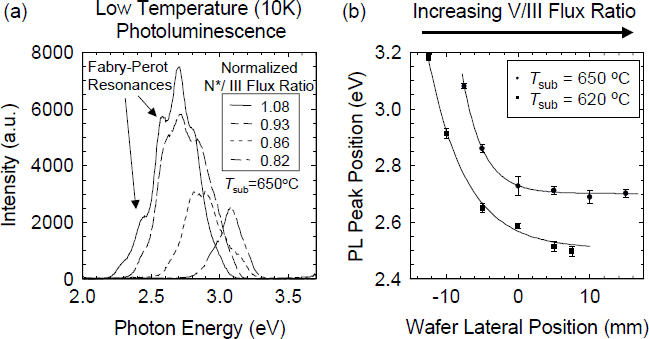
Low temperature PL measurements from the second set of samples are also consistent with this segregation/desorption interpretation and provide insight into the effect of growth temperature and V/III flux ratio on the optical quality of the samples. The observed PL spectra from these samples are single, broad peaks, often with indications of Fabry-Perot resonances. Both the PL intensity and peak positions are strongly affected by the substrate temperature and incident V/III flux ratio. At temperatures below approximately 590°C, the luminescence intensity decreases rapidly; at the lowest temperature of this study (540°C), no PL spectra could be observed. The effect of the N*/III flux ratio on the PL spectra is illustrated in Fig. 3(a). The PL spectra are observed to shift to lower energy and the PL intensity is observed to increase for higher N*/III flux ratios (over the limited range of flux ratios used in this study). Fig. 3(b) shows the PL peak position as a function of the lateral position on the wafer (N*/III flux ratio) for temperatures above 590°C. Consistent with the segregation/desorption interpretation, the PL peak position is observed to move to lower energy as either the substrate temperature is decreased, or as the N*/III ratio is increased. In general, the measured PL peak positions appear at lower energies than expected based on estimates using reported[Reference McCluskey, Van de Walle, Master, Romano and Johnson12] band-bowing parameters and the In compositions determined by HRXRD. This is most likely attributable to unintentional inhomogeneity within the InGaN layers. Lastly, a higher optical quality (luminescence efficiency) is observed for higher V/III flux ratios and higher growth temperatures.

Figure 3. (a) Effect of incident N*/III flux ratio on photoluminescence spectra. Spectra are observed to shift to lower energies as the N*/III flux ratio increases. In general, a substantial improvement in optical quality (luminescence intensity) is observed upon going from flux-limited to kinetically-limited growth regime (see text).

Summary

In x Ga1− x N/GaN superlattices structures have been grown by RF-MBE methods to study the effects of substrate temperature and incident V/III flux ratio on In incorporation efficiency. Below a critical substrate temperature (≈ 590°C for growth rates on the order of 0.3μm/h), In incorporation is efficient but material quality as assessed by photoluminescence is very poor. Above this temperature, In incorporation efficiency is found to decrease sharply according to a Boltzmann factor, with an activation energy value which is affected by the N*/III flux ratio during growth. At fixed flux ratio, In incorporation efficiency decreases by over an order of magnitude between 590°C and 670°C, and at the latter temperature, a flux-ratio increase of only ∼20% results in nearly an order of magnitude increase in incorporation efficiency. Optical quality markedly improves above the critical temperature, and to a lesser extent at high temperature improves with increasing flux ratio as well. Results are consistent with thermally activated processes of In surface segregation and surface desorption as the microscopic mechanism of In loss during MBE growth.

Acknowledgements

The authors gratefully acknowledge the support of the Army Research Office under Grant No. DAAH04-94-G-0393. Additionally, one of us (M.L.O.) wishes to acknowledge financial support provided by the NASA Oklahoma Space Grant Consortium and the DoE EPSCoR Traineeship Program.

References

. Böttcher, T., Einfeldt, S., Kirchner, V., Figge, S., Heinke, H., Hommel, D., Selke, H., and Ryder, P. L., Appl. Phys. Lett. 73, 3232 (1998).CrossRefGoogle Scholar
. Doppalapudi, D., Basu, S. N., Ludwig, K. F. Jr., and Moustakas, T. D., J. Appl. Phys. 84, 1389 (1998).CrossRefGoogle Scholar
. Singh, R., Doppalapudi, D., Moustakas, T. D., and Romano, L. T., Appl. Phys. Lett. 70, 1089 (1997).CrossRefGoogle Scholar
. Yang, B., Brandt, O., Jenichen, B., Müllhäuser, J., and Ploog, K. H., J. Appl. Phys. 82, 1918 (1997).CrossRefGoogle Scholar
. Ho, I.-H. and Stringfellow, G. B., Appl. Phys. Lett. 69, 2701 (1996), and references therein.CrossRefGoogle Scholar
. Müllhäuser, J. R., Brandt, O., Trampert, A., Jenichen, B., and Ploog, K. H., Appl. Phys. Lett. 73, 1230 (1998).CrossRefGoogle Scholar
. Widmann, F., Daudin, B., Feuillet, G., Pelekanos, N., and Rouvière, J. L., Appl. Phys. Lett. 73, 2642 (1998).CrossRefGoogle Scholar
. Chen, H., Smith, A. R., Feenstra, R. M., Greve, D. W., and Northrup, J. E., MRS Internet J. Nitride Semicond. Res. S1, G9.5 (1999).Google Scholar
. O’Steen, M. L., Fedler, F., and Hauenstein, R. J., Appl. Phys. Lett. 75, 2820 (1999).CrossRefGoogle Scholar
. Hauenstein, R. J., Collins, D. A., Cai, X. P., O’Steen, M. L., and McGill, T. C., Appl. Phys. Lett. 66, 2861 (1996).CrossRefGoogle Scholar
. Bandic, Z. Z., Hauenstein, R. J., O’Steen, M. L., and McGill, T. C., Appl. Phys. Lett. 68, 1510 (1996).CrossRefGoogle Scholar
. McCluskey, M. D., Van de Walle, C. G., Master, C. P., Romano, L. T., and Johnson, N. M., Appl. Phys. Lett. 72, 2725 (1998).CrossRefGoogle Scholar
Figure 0

Figure 1. (a) Representative θ-2θ scan of a superlattice sample about the GaN (0002) diffraction peak. Inset: Linear regression analysis of the quantity 2sin(θn)/λ vs. superlattice peak index n, used to determine the superlattice period L and average Bragg-plane spacing . (b) Depiction of MBE growth geometry and in-plane axis used for laterally resolved X-ray measurements

Figure 1

Figure 2. Spatial variations, due to local V/III flux ratio, in (a) superlattice period L, (b) mean alloy composition , (c) effective GaN growth rate, and (d) effective InN growth rate, for growth under two different N* fluxes. (e) Effect of Tsub on , for slightly differing V/III flux ratios. At low Tsub, approaches the nominal value determined by incident fluxes while at high Tsub, is limited via rate kinetics of thermally activated In-loss mechanisms (surface segregation + surface desorption), which freeze out here at ≈590°C. The kinetic barrier to In loss is extremely sensitive to N*/III ratio (growth-surface stoichiometry).

Figure 2

Figure 3. (a) Effect of incident N*/III flux ratio on photoluminescence spectra. Spectra are observed to shift to lower energies as the N*/III flux ratio increases. In general, a substantial improvement in optical quality (luminescence intensity) is observed upon going from flux-limited to kinetically-limited growth regime (see text).