


1. Introduction
Studies of mixed group-V alloys like GaNAs are currently of great fundamental interest, and they may also offer application possibilities for optoelectronic devices. The large difference in lattice constant (20%) between GaAs and GaN leads to a nonlinear behavior of the energy gap versus nitrogen concentration. Recent optical measurements show a considerable red shift of the band edge in GaNxAs1−x alloys with increasing x for low x values Reference Weyers, Sato and Ando[1] Reference Weyers and Sato[2] Reference Pozina, Ivanov, Monemar, Thordson and Andersson[3]. This property may be used for applications of GaNxAs1−x as a novel III-V compound material integrated with Si Reference Kondow, Uomi, Hosomi and Mozume[4]. Growth of GaNxAs1−x with a nitrogen concentration varying in the broad range 0 < x < 1 can give a promising semiconductor alloy for fabrication of light-emitting devices covering the whole visible and ir spectrum.
Theoretical predictions of the GaNxAs1−x electronic structure depend strongly on the model used and show contradictory results. Sakai et al. Reference Sakai, Ueta and Terauchi[5], using Van Vechten's model Reference Van Vechten[6], and Neugebauer and Van de Walle Reference Neugebauer and Walle[7], using first-principles total energy calculations, predicted a negative band gap for N concentrations in the range 0.09 - 0.87 and 0.16 - 0.71, respectively. In contrast, calculations of Bellaiche et al. Reference Bellaiche, Wei and Zunger[8], based on a supercell representation of the alloy, confirmed the previous suggestion of Wei and Zunger Reference Wei and Zunger[9] that GaNxAs1−x is a semiconductor rather than a semimetal for the whole range of x, and that the optical bowing parameter is strongly composition dependent, unlike the case of conventional III-V alloys.
The band gap energy estimated from photoluminescence and absorption measurements follows a linear dependence on nitrogen concentration x up to 4% Reference Weyers, Sato and Ando[1] Reference Weyers and Sato[2] Reference Pozina, Ivanov, Monemar, Thordson and Andersson[3] Reference Kondow, Uomi, Hosomi and Mozume[4] Reference Kondow, Uomi, Niwa, Kitatani, Watahiki, Yazawa, Hosomi and Mozume[10], which implies a constant bowing parameter. However, Bi and Tu Reference Bi and Tu[11] have shown from optical absorption measurements that the bowing parameter of GaNxAs1−x is composition dependent for x = 0 - 0.15. Transmission electron microscopy studies of the microstructure of GaNAs reveal a tendency to phase separate Reference Foxon, Cheng and Novikov[12] Reference Xin, Brown, Dunin-Borkowski, Humphreys, Cheng and Foxon[13] Reference Sato[14] if the nitrogen content is above the nitrogen solubility level in the ternary alloy Reference Kondow, Uomi, Kitatani, Watahiki and Yazawa[15].
In this work we report the results of low temperature optical characterization of GaNxAs1−x grown by MBE with different nitrogen concentrations. We discuss the optical transitions close to the GaAs- and the GaN- band gap, respectively. X-ray diffraction (XRD), photoluminescence (PL) and Raman spectroscopy confirm a phase separation in the GaNxAs1−x layers. We estimate the band-gap energy dependence on nitrogen concentration and the value of the bowing parameter.
2. Experimental
GaNxAs1−x layers of different thickness (1 − 6 μm) were grown by MBE on semi-insulating GaAs substrates. The samples can be divided into three categories depending on the average nitrogen content in the layers: (i) GaAs:N-layers containing low concentrations of isovalent doping nitrogen, (ii) As-rich GaNxAs1−x layers with average x values from 0.01 up to 0.3, and (iii) As-poor GaNxAs1−x layers with average nitrogen concentration of x avg>0.95. Further details about the growth procedure can be found in Ref. Reference Thordson, Zsebök, Södervall and Andersson[16].
The average composition was determined by secondary ion mass spectrometry (SIMS), using Cs+ as primary ions. The single crystalline structure was characterized by double crystal XRD. Figure 1(a) illustrates a typical x-ray diffraction spectrum of a GaNAs sample with an average nitrogen composition of ~ 8.6% obtained from the SIMS measurements. Analysis of XRD spectra for the epitaxial layers distinctly indicates the presence of three different crystalline phases: there are two features at ~ 33°, corresponding to the GaAs and GaNxAs1−x, and a rather broad peak at ~ 43°, identified as GaN(As), i.e. GaN with dissolved arsenic. The position of the GaNxAs1−x peak depends on the average nitrogen concentration. Applying the linear Bragg and Vegard's law, the N-composition is about 1.85% for this sample, which is much smaller than indicated by the SIMS measurements. The discrepancy between the nitrogen content as determined by SIMS and by XRD becomes more significant with increasing average N-composition and indicates the presence of phase separation. The maximum concentration we could achieve was x = 3.6% in As-rich GaNxAs1−x layers as determined by XRD. For this sample, the SIMS data Reference Thordson, Zsebök, Södervall and Andersson[16] gives much higher average nitrogen content in the epilayer, ~ 36%. For As-poor GaNxAs1−x layers we observed only features close to GaN, shown in Figure 1(b) for two samples. The peak maximum is shifted from the GaN-position and the linewidth becomes broader with increasing arsenic concentration, i.e. formation of GaN(As) occurs. Finally, for the samples with low average nitrogen concentration (x < 1%) there is no GaN-diffraction peak. In the following we denote nitrogen composition determined by SIMS as x avg, and by XRD as x.

Figure 1. The XRD spectrum of the GaNxAs1−x sample with 1.85% nitrogen (a), and XRD spectra for two GaN(As) layers with low arsenic content of 0.3% and 4%, respectively (b).
The layers of GaNxAs1−x with thickness of a few μm are relaxed, as shown by XRD-measurements (we could not see any satellite fringes around the GaAsN-peak). However, one cannot exclude the possibility that there might be some random strain contribution, since different phases exist in the layer.
3. Results and Discussion
We have studied the low temperature photoluminescence in GaNAs samples over a wide range of compositions, and found that PL spectra are rather different for the three types of samples.
Figure 2 illustrates a typical photoluminescence spectrum of the GaAs:N sample with low (doping range) average nitrogen concentration. The luminescence exhibits a pronounced GaAs spectrum with an excitonic transition at 1.514 eV close to the GaAs band gap, together with a dominating line at E=1.492 eV corresponding to the free-to-bound transition involving the C-acceptor. We observed also additional GaAs-related features connected with emission of the CuGa-acceptor (1.356 eV) and its two LO-phonon replicas at 1.320 eV and 1.284 eV, respectively. In summary, no clear N-related features are observed.
As-rich GaNxAs1−x samples reveal either a relatively weak luminescence corresponding to the GaAs-phase, or they show a very broad emission band with maximum at ~ 0.8 eV, as Figure 3 demonstrates for a layer with x avg=0.066. The appearance of such an emission is usual for highly defective material, and is an additional proof that with increasing of N-content in the layers the concentration of defect states dramatically increases. It is well known that in such material the near-band-gap excitonic luminescence is suppressed, thus it is difficult to expect any pronounced luminescence corresponding to the GaNxAs1−x solid solution phase. The structure observed in the spectral range 0.86 − 0.94 eV in Figure 3 is due to absorption by water vapor.
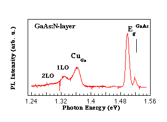
Figure 2. The low temperature (T=2 K) photoluminescence spectrum in the infrared region for the GaAs:N sample with an isoelectronic nitrogen doping concentration of 1018 cm−3.

Figure 3. Typical defect emission band in the As-rich GaNxAs1−x-layers with an average nitrogen concentration of 6.6%.
In the ultraviolet region we have observed similar spectra for GaAs:N layers and for As-rich GaNxAs1−x layers. These spectra consist of two relatively narrow (7 meV wide) lines with peak positions at 3.31 eV and 3.364 eV, respectively. Figure 4 illustrates a spectrum from a layer with 8.6% average nitrogen concentration. The nature of these lines has been frequently discussed in the recent literature on GaN Reference Hong, Pavlidis, Brown and Rand[17] Reference Wetzel, Fischer, Kruger, Haller, Molnar, Moustakas, Mokhov and Baranov[18], however, there is no satisfactory explanation of their origin. Attempts have been made to attribute these lines to localized excitons in wurtzite GaN Reference Wetzel, Fischer, Kruger, Haller, Molnar, Moustakas, Mokhov and Baranov[18], to the shallow bound exciton in the cubic GaN Reference Hong, Pavlidis, Brown and Rand[17], and recently to quantum confined states in cubic inclusions in GaN Reference Rieger, Dimitrov, Brunner, Rohrer, Ambacher and Stutzmann[19]. Similar features have also been observed in materials apparently containing no GaN at all. These lines may therefore be connected with an unknown localized defect level Reference Dai, Fu, Xie, Fan, Hu, Schrey and Klingshirn[20]. As stated above we have observed the same spectra for a GaAs layer with doping concentration of nitrogen, where there is unlikely to be a GaN-phase.

Figure 4. The low temperature (T=2 K) photoluminescence in the ultraviolet region for an As-rich GaNxAs1−x layer with 8.6% average nitrogen concentration.
Arsenic-poor GaNAs layers, on the contrary, provide different spectra in the ultraviolet region, but have the common characteristic of a broad emission band. Figure 5(a) presents spectra for two As-poor GaN(As) samples with average arsenic concentration 0.3 % and 4 %, respectively. A red shift of the peak position and a drastic widening of the bandwidth with decreasing nitrogen concentration indicate a near-band-gap transition in the cubic GaNAs phase. This result is consistent with XRD data shown in Figure 1(b) for As-poor GaN(As) samples. The broadening is associated with inhomogeneity of the layers with increasing arsenic content in the alloy. The shape and peak position of the emission band from the layer with low arsenic concentration 0.3% is similar to that for cubic GaN Reference Godlewski, Ivanov, Bergman, Monemar, Barski, Langer, Pensl, Morkoc, Monemar and Janzen[21], as Figure 5(b) illustrates. It confirms the XRD data about the cubic symmetry of the structures.

Figure 5. Photoluminescence measured at T = 2 K for two As-poor GaNxAs1−x layers with arsenic concentration of 0. 3% and 4%, respectively, (a), and a photoluminescence spectrum of the cubic GaN taken from Ref. 21 is shown for comparison (b).
For the As-rich GaNxAs1−x layers, the photoluminescence data do not give much information about near-band-gap transitions to confirm the presence of different phases in the samples. Therefore we use Raman spectroscopy as a rapid and sensitive method to determine the phase composition of these GaNxAs1−x layers. A depolarized Raman spectrum excited at 3.53 eV is shown in Figure 6 for the sample with 19% average nitrogen concentration. It clearly reveals two narrow features at 292 cm−1 and 740 cm−1 with a full width at half maximum (FWHM) of 10 and 20 cm−1, respectively. The position of the first peak fits with the well-known LO phonon mode in GaAs. The line observed at 740 cm−1 corresponds to the LO phonon frequency in cubic GaN Reference Giehler, Ramsteiner, Brandt, Yang and Ploog[22]. Recent experiments on Raman scattering in amorphous GaN0.3As0.7 show a very broad weak feature around 750 cm−1 with FWHM of 280 cm−1 Reference Bandet, Aguir, Lollman, Fennouh and Carchano[23]. Thus, we can conclude that in our As-rich GaNxAs1−x layers, crystalline phases of cubic GaAs and cubic GaN coexist, in agreement with the XRD results. However, we have not observed any specific manifestation of the GaNxAs1−x ternary alloy in the Raman spectra, probably because the vibrational LO mode in GaAs is close to the one in the solid solution with very low nitrogen concentration x = 0.017 (as determined by XRD). A recent Raman scattering study of GaNxAs1−xlayers with x = 0 − 0.05 Reference Mintairov, Blagnov, Melehin, Faleev, Merz, Qiu, Nikishin and Temkin[24] demonstrated the presence of diagonal components for both the GaAs- and GaN-type optical phonons.

Figure 6. Depolarized Raman spectrum measured at room temperature for an As-rich GaNxAs1−x layer with 8.6% average nitrogen concentration.
In addition, we present in Figure 7 the estimation of the band gap energy as a function of the nitrogen concentration in the GaNxAs1−xalloy. Our experimental data of Eg for low x (up to 0.04) extracted from absorption measurements Reference Pozina, Ivanov, Monemar, Thordson and Andersson[3] are shown as solid circles. Also shown in the figure are results of PL measurements for x close to 1 (open circles). The line presents the fitting of the experimental values of Eg assuming that the GaNxAs1−x band gap composition dependence obeys the simple parabolic law:
where b is the bowing coefficient, Eg= 1.519 eV for GaAs and Eg= 3.3 eV for cubic GaN Reference Ramirez-Flores, Navarro-Contreras, Lastras-Martinez, Powell and Greene[25]. We conclude from these data that the bowing parameter is constant and equals -18 eV. A good correspondence between calculations and experiments both for low x and x close to 1 suggests that at least in the investigated range of x the bowing coefficient in GaNxAs1−x is composition independent. Assuming that the bowing parameter is a constant for all x it is reasonable to expect semimetallic properties of the GaNxAs1−xalloy for a broad range of x between approximately 12% and 75%.

Figure 7. The band-gap energy of GaNxAs1−x as a function of nitrogen concentration. Experimental results are shown by the solid circles for absorption data and by the open circles for the PL measurements. The solid line is fitting of Eg using parabolic law with b = -18 eV (the part of the calculated curve in the inexperienced region of nitrogen concentrations is shown by the dashed line).
Our values of the GaNxAs1−x band-gap energy and the value of the bowing coefficient are in a good agreement with calculations by Sakai et al. Reference Sakai, Ueta and Terauchi[5] and Neugebauer and Van de Walle Reference Neugebauer and Walle[7] for the relaxed superlattice and very close to the recent experimental result of Francoeur et al. Reference Francoeur, Sivaraman, Qiu, Nikishin and Temkin[26]. They determine b=-19 eV for the strained GaNAs layers Reference Qiu, Nikishin, Temkin, Faleev and Kudriavtsev[27] Reference Qiu, Jin, Francoeur, Nikishin and Temkin[28] with nitrogen concentration up to ~3%.
4. Conclusion
In conclusion, GaNxAs1−x layers prepared by MBE have been characterized by XRD, SIMS, PL, and Raman scattering., We divided the samples into three groups according to the nitrogen content: (i) GaAs:N with doping concentration of nitrogen, (ii) As-rich GaNxAs1−x with average x<0.3, and finally As-poor GaNxAs1−x with x close to 1. We have found that different phases, which have been identified as GaAs, GaN and the ternary alloy GaNxAs1−x, are present in samples with nitrogen concentration exceeding the N solubility limit. We have discovered a strong red shift of the PL peak energy from the GaN band gap for As-poor GaNxAs1−x layers with increasing As content. We interpret this emission as a near-band-gap transition in GaNxAs1−x layers with x close to 1. Analysis of the dependence of Eg on x for low x and for x close to 1 allows us to assume a constant bowing parameter -18 eV for the GaNxAs1−x ternary compound alloy.


