


Introduction
GaN (gallium nitride) and its alloys are promising as a wide band-gap, high temperature semiconducting material for application as blue- and ultraviolet-light-emitting devices, and high power/high frequency devices [Reference Nakamura, Senoh, Nagahama, Iwasa, Yamaha, Matsushita, Kiyohu and Sugimoto1]. GaN materials are grown on various foreign substrates with large lattice mismatch and significant differences of thermal expansion coefficient. Such heteroepitaxial structures are inevitably accompanied by the introduction of various kinds of extended defects such as dislocations, prismatic stacking faults, etc. [Reference Brown2]. It is well recognized that the reduction in density of threading defects does lead to improvement of optical and electrical properties of GaN [Reference Keller, Keller, Wu, Heying, Kapolnek, Speck, Mishra and Den-Baars3]. Thus, efforts are being made in controlling film stress to reduce the occurrence of detrimental defects during GaN hetero-epitaxial growth to obtain high performance devices. Understanding of dislocation behavior in this material is also indispensable.
The obstacle to conducting such an investigation has been the difficulty in growing bulk GaN crystal of a suitable size for deformation test. A few investigations are available on dislocation motion or hardness of GaN at room temperature. Drory et al. [Reference Drory, Ager, Suski, Grzegory and Porowski4] measured the hardness and fracture toughness of GaN by a conventional hardness test. Nowak et al. [Reference Nowak, Pessa, Suganuma, Leszczynski, Grzegory, Porowski and Yoshida5] recently evaluated the yield strength of GaN by nano-indentation. Maeda et al. [Reference Maeda, Suzuki, Ichihara, Nishiguchi, Ono, Mera and Takeuchi6] observed the viscous motion of dislocations under electron irradiation using a transmission electron microscope operating at 200kV. Yonenaga [Reference Yonenaga7] presumed empirically that the activation energy for dislocation motion in GaN is presumed to be 2 eV.
This paper reports the hardness of GaN at elevated temperature in comparison with those of other typical materials such as Si, GaAs, etc. As far as we know, this is the first information on the mechanical strength of GaN at elevated temperature and is important as a basis for the control of dislocation generation during crystal growth.
Experiment
GaN single crystals were prepared from a high quality GaN thick film grown on a 2-inch diameter (0001) sapphire substrate by using hydride vapour phase epitaxy (HVPE) together with the selective growth through SiO2 windows by means of the facet initiated epitaxial lateral overgrowth (FIELO) technique. The details on the growth procedure are described elsewhere [Reference Usui, Sunakawa, Sakai and Yamaguchi8]. Finally, the thick grown layer was removed from the substrate. As a result, crack-free GaN single crystals of 0.5 mm thickness with mirror-like surfaces were successfully obtained and were sufficiently thick to be regarded as being bulk material. The density of grown-in dislocations was as low as 107 cm−2 [Reference Sakai, Sunakawa and Usui9]. Hardness measurements on the crystals were carried out by the Vickers indentation method using a pyramidal diamond indentor. The applied indentation load P was 0.5 - 5 N, and the dwell time 30 seconds, for every temperature tested in the range from room temperature to 1200°C in a high purity Ar gas atmosphere. Four indents were formed at every temperature for the Ga ( 0001) and N ( 000
Results and Discussion
Figure 1(a) and 1(b) show an optical micrograph of the indent, formed for the N (000

Figure 1. Optical micrograph of Vickers indent of bulk single crystal GaN (a) at RT with an applied load of 1 N and dwell time of 30 s and (b) at 200°C with 0.5 N and 30 s.
Hardness H v was estimated from the load P and diagonal lengths 2a, measured by optical microscopy, of the indent using the following relation:
The fracture toughness K c was also determined from the radial crack length c:
where E is the Young’s modulus and ξ is a calibration constant (= 0.016) for brittle materials.
The hardness is comparable for the Ga (0001) and N ( 000
At RT the hardness of GaN is estimated to be 10.8 GPa under the applied load 0.5 - 3 N, about twice the value of GaAs, which is similar to that 12 GPa reported by Drory et al. [Reference Drory, Ager, Suski, Grzegory and Porowski4]. In their experiments the applied load was 2 N. Moreover, the fracture toughness is estimated to be 1.1 MPa•m under the applied load range 0.5 - 5 N using Eq. (2) with E = 295 GPa recently reported [Reference Nowak, Pessa, Suganuma, Leszczynski, Grzegory, Porowski and Yoshida5]. Table I summarises the hardness of various semiconductor (111) or (0001) surfaces, together with that of sapphire (0001) surfaces [Reference Farber, Yoon, Lagerlöf and Heuer10], at RT.
Figure 2 shows the hardness Hv of GaN, obtained with an applied load of 0.5N and dwell time of 30s, plotted against reciprocal temperature in comparison with other material (111) or (0001) surfaces. In the whole temperature range investigated, the hardness of GaN shows a gradual decrease from RT to 500°C, then something of a plateau in the range 500 - 1000°C and then a steep decrease. Such the temperature dependence is similar to that of 6H-SiC and sapphire, with the similar hcp-based structure, although the temperature range and hardness magnitudes of SiC or sapphire are higher than those of GaN. The plateau may appear in relation to the operation of different slip systems in the crystal structure. It is found that GaN is harder than GaAs in the whole temperature range investigated and that at temperatures lower than 600°C, the hardness of GaN is comparable to, or a little lower than, that of Si. Surprisingly, up to about 1100°C, GaN maintains its hardness and is harder than Si. Indeed, Si and GaAs show a steep decrease in hardness from 500°C and 200°C, respectively, with increasing temperature, which means the beginning of macroscopic dislocation motion and plastic deformation. Thus, the result for GaN implies that such macroscopic dislocation motion and plastic deformation may start at around 1100°C.
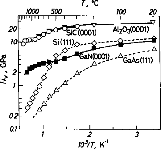
Figure 2. Vickers hardness of bulk single crystal GaN plotted against reciprocal temperature, with an applied load of 0.5 N and dwell time of 30 s, together with those of Si, GaAs, and 6H-SiC. The hardness of sapphire obtained with 2 N and 15 s is superimposed [Reference Farber, Yoon, Lagerlöf and Heuer10].
Table I. Vickers hardness of GaN and various semiconductors at room temperature or 300°C with an applied load of 0.5 N and dwell time of 30 s. The hardness of sapphire obtained with 2 N and 15 s is also included [Reference Farber, Yoon, Lagerlöf and Heuer10].

The present results imply that GaN has a higher mechanical stability during device processing at high temperatures than Si, GaAs, and possibly other III-V compounds with the sphalerite structure. Unfortunately, a more complete physical understanding of hardness in order to derive the dynamic properties of dislocations, is still lacking in absence of sufficient theory and is a task in the future. However, we recognise that the present data provide a useful measure of material strength at elevated temperature. Further work is needed to determine dislocation mobilities within GaN bulk crystals under defined stress distribution.
Conclusion
A Vickers hardness for crack-free bulk single crystal GaN was determined in the temperature range 20 - 1200°C. The hardness of GaN is c10.8 GPa at room temperature and is omparable to that of Si at temperatures lower than 600°C. Up to about 1100°C, GaN maintains its harness, being mechanically stable in comparison with Si and GaAs.
Acknowledgement
The authors are grateful to Prof. P. Pirouz of Casewestern Reserve University for the supply of SiC crystals.


