Introduction
The InxGa1−xN alloys have been used as an active layer material of InGaN based blue and green light emitting diodes (LEDs) and laser diodes (LDs) because they cover a wide band-gap ranging from 1.9 to 3.4 eV. Especially, InGaN/GaN quantum well (QW) is center of interest on account of their huge applications in high brightness LED, [Reference Nakamura, Senoh, Nagahama, Iwasa, Yamada, Matsushita, Sugimoto and Kiyoku1] cw blue LD, [Reference Nakamura, Senoh, Nagahama, Iwasa, Yamada, Matsushita, Sugimoto, Kiyoku, Umomoto, Sano and Chocho2] and optoelectronic devices. Nevertheless, the emission and growth mechanisms of InGaN/GaN QW structure is still equivocal and debating.
In recent, a few research groups have suggested that the optical emission mechanism in InGaN/GaN QW should be due to InGaN quantum dot (QD). [Reference Keller, Keller, Minsky, Bowers, Mishra, DeenBaars and Seifert3] Another groups, on the other hand, asserted that the emission from the InGaN/GaN QW stems from piezo-electric effects, [Reference Liu, Teo, Li, Chua, Uchida, Tokunaga, Akutsu and Matsumoto4] quantum confined Stark effects [Reference Takeuchi, Sota, Sakai, Amanoa, Akasaki, Kaneko, Nakagawa, Yamaoka and Yamada5] or potential fluctuation of InGaN QW.
In this work, we investigate the time dependent 2D to 3D mophological evolution of InGaN thin films grown by metalorganic chemical vapor deposition (MOCVD) through atomic force microscopy (AFM), high resolution transmission electron microscopy (HRTEM) measurements. Besides, their related optical emission characteristics in InGaN/GaN SQW using photoluminescence (PL) measurement.
Experiments
All InGaN/GaN QW structures used in this study were grown by low pressure horizontal MOCVD. InGaN/GaN SQW structures are consisted of a GaN nucleation layer with a nominal thickness of 25 nm grown at 560 °C, a Si-doped GaN layer with a thickness of 1.8 um grown at 1100 °C, a low-temperature grown GaN with a thickness of 5 nm, InGaN SQW applying different growth conditions, and a 30 nm-thick GaN capping layer grown at 1100 °C. The precursors of Ga, In, Si, and N are trimethylgallium, trimethylindium, silane, and ammomia, respectively.
Results and Discussion
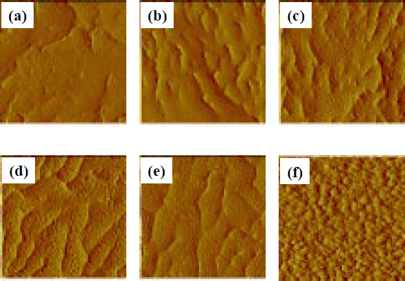
Figure 1 (a) – (f) show the AFM images of morphological evolution of InGaN thin films grown at 800 °C, which are dependent on the growth times (thickness) from 0 sec to 3600 sec. Typical surface shape for n-type GaN, including steps, terraces, and surface dislocations, is shown in Fig. 1 (a). The small surface dislocations observed are 37 nm in size and 0.5 - 1 nm in height. The density of surface dislocations is 4 − 5 × 109 cm−2, which shows good agreement with the dislocation density measured by the TEM. Many of them are lie along the step boundaries. As the nominal thickness of InGaN films increase from 0.15 to 1.15 nm, one can clearly see that 2 D (corresponding to wetting layer) to 3 D (self-assembled QD) transition, which is direct evidence of Stranski-Krastanov (S-K) growth mode of InGaN epilayer. For the case of QDs shown in the InGaN film with the thickness of 0.57 nm and 1.15 nm, the average lateral size and height of dots are 73 nm, 2 nm, and 78 nm, 3.7 nm, respectively. Especially, the density (4 × 109 cm−2) of QDs shown in Fig. 1 (c) is nearly same with that of surface dislocations of low-temperature grown GaN. However, we have confirmed they have no correlation each other (see Fig. 2 (a)). If the thickness more increases, the size of the InGaN nano-scale dots is increased and the InGaN film shows polycrystalline growth mode or cluster formation.

Figure 1 , AFM images of InGaN films with the growth time (nominal thickness) of (a) 0 sec (0 nm), (b) 3 sec (0.15 nm), (c) 12 sec (0.57 nm), (d) 24 sec (1.15 nm), (e) 48 sec (2.3 nm), and (f) 3600 sec (400 nm). Scan areas are 4 × 4 um2.
From the x-ray photoelectron spectroscopy measurement (not shown here), we observed that In 3d peaks intense with increasing the thickness of InGaN thin films. This result shows that In surface segregation is occurred during the InGaN growth[Reference Hiramatsu, Kawaguchi, Shimizu, Sawaki, Zheleva, Davis, Tsuda, Taki, Kuwano and Oki6].
Figure 2 (a) and (b) show a plan-view HRTEM and a cross sectional HRTEM (X-HRTEM) image of the sample in Fig. 1 (c). The most important feature in (a) is that the nano-scale dots are formed irrespective of dislocation indicated by an arrow. Especially, knowledge of the shape of self-organized InGaN/GaN QDs is needed to constrain theoretical calculations of the process formation as well as electronic structure. For the heteroepitaxial growth suffering large lattice mismatch like InAs/GaAs and Ge/Si, several quantum dot shapes, namely conical[Reference Marzin and Bastard7], square-base pyramid[Reference Jiang and Singh8], prism-like cluster[Reference Mo, Savage, Swartzentruber and Lagally9], triangular shape [Reference Lobo and Leon10] etc., have been reported. Figure (b) shows that the InGaN nano-scale dot with trapezoidal shape are formed on InGaN wetting layer without dislocations and also has {1-102} facet planes inclined by 35° with respect to the (0002) surface.

Figure 2 , (a) Plan-view HRTEM weak beam image and (b) X-HRTEM image of 0.57 nm-thick InGaN thin film. Arrow shown in (a) indicates dislocations.
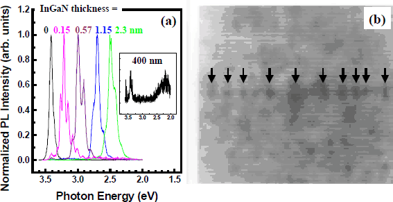
Fig 3 (a) shows the room temperature PL spectra of InGaN/GaN SQW with the InGaN thickness described in Fig. 1. The FWHM values are 70 – 140 meV. The PL spectra were recorded using the 325 nm line of a He-Cd laser with an excitation power density of 2 W/cm2. As we changing InGaN QW thickness from 0 to 2.3 nm, broad area spectra covering from UV (3.4 eV) to green (2.45 eV) are observed. Nano-scale dots formed in InGaN SQW with the thickness of 0.57 nm are displayed in Fig. 3 (b), which definitely affect the emission from the InGaN SQW. Therefore, in order to explain the peculiar behavior of large red shift (900 meV) shown in (a), we have to consider not only both QD confinement effect and QW thickness variation but also In surface segregation effect, piezoelectric effect etc..

Figure 3 , (a) Room temperature PL spectra of InGaN/GaN SQW with various InGaN thickness, and (b) X-HRTEM image of InGaN/GaN SQW with the InGaN QW thickness of 0.57 nm. Arrows point out the formed InGaN nano-scale dots.
Temperature dependent PL for the InGaN SQWs with the InGaN thickness of 0.15, 0.57, and 2.3 nm was performed in the temperature range of 5 K to 300 K. In Fig. 4, the variations of integrated PL intensities of respective sample are plotted as functions of the inverse of temperatures. The thermo-activation energy for bound excitonic emission obeys the following relation[Reference Pankove11]:
where I(T) is the integrated PL intensity at temperature of T and I0 and C are constants. kB is Boltzmann’s constant. Ea is equal to the thermo-activation energy. The solid lines in Fig. 4 denote the least-square fit of the experimental data by Eq. (1). For the cases of InGaN SQW specimens with the InGaN thickness of 0.15, 0.57, and 2.3 nm, the estimated thermo-activation energies are 35, 53, and 54 meV, respectively. This result reveals that PL emission from InGaN SQW samples embedded on InGaN 3D nano-scale dots suffer more additional quantum confinement energy of nearly 20 meV than the case of embedded on InGaN 2D wetting layer.

Figure 4 , Arrhenius plot of the integrated PL intensity of the InGaN SQW samples with the InGaN QW thickness of 0.15 (down triangle), 0.57 (circle), and 2.3 nm (square), respectively
Summary
Thin layers of InGaN as a function of thickness were grown by MOCVD and characterized using AFM and HRTEM. InGaN thin films grown on GaN reveals a Stranski-Krastanov growth mode,. From the plan-view HRTEM measurement, we observed the creation of InGaN self-assembled QD is not related with dislocations. We have also found that the formed InGaN nano-scale dots have the trapezoidal shape with a {1-102} facet. Visible spectral range from UV to green was easily obtained by changing InGaN quantum well thickness up to 2.3 nm. From the integrated PL intensity analysis, emission from InGaN SQW samples embedded on InGaN 3D nano-scale dots suffer more additional quantum confinement than the case of embedded on InGaN 2D wetting layer.
Acknowledgements
This work has been supported by the KOSEF and the MOST of Korea through the Semiconductor Physics Research Center at Chonbuk National University.