


1. Introduction
GaN and AlGaN are wide, direct bandgap semiconductors ideally suited for the fabrication of solid state ultraviolet (UV) detectors that have applications in both flame detection and threat warning systems. Much work to date has focused on GaN photoconductors Reference Khan, Kuznia, Hove and Olson[1] Reference Goldenberg, Zook and Ulmer[2] Reference Zook, Goldenberg and Spencer[3]. Although photoconductive detectors have the desirable property of internal gain, they suffer from well known drawbacks which include high dark currents, DC drift, slow response time, and occasionally spurious photoresponse at long wavelengths. Recently, relatively fast photovoltaic UV detection using GaN p-n diodes or Schottky diodes has been demonstrated Reference Van Hove, Hickman, Klaassen, Chow and Ruden[4] Reference Chen, Yang, Osinsky, Gangopadhyay, Lim, Anwar, Khan, Kuksenkov and Temkin[5] Reference Zhu, Salvador, Kim, Fan, Lu, Tang, Morkoc, Smith, Estes, Goldenberg, Yang and Krishnankutty[6]. A key advantage of III-nitride detectors over competing devices based on semiconductors with smaller bandgaps (for example UV-enhanced Si photodetectors) is the long wavelength response cut-off which is directly related to the bandgap of the material in the active region and thus does not require external filters. For many applications, however, an additional short wavelength cut-off defining a UV band is also advantageous or even required. In this paper we report on the development of GaN/Al0.1Ga0.9N heterojunction photodiodes that have high quantum efficiency (over 80%) in a UV band from 352nm to 362nm, with four orders of magnitude rejection between the peak response and longer visible wavlengths and nearly three orders of magnitude rejection of shorter wavelengths. The devices also have low dark currents at moderate reverse voltages (V > -10V).
2. Device Fabrication
The p-i-n diode structure shown in Figure 1 was grown on basal plane sapphire using low pressure Metalorganic Chemical Vapor Deposition (MOCVD). Chemical precursors used included triethylgallium, triethylaluminum, ammonia, biscyclopentadieynl magnesium (p-dopant) and silane (n-dopant). The n-Al0.1Ga0.9N/i-GaN/p-GaN heterostructures were grown on thin AlN buffer layers. Carrier concentrations in the n- and p-type layers were typically 2×1018cm−3 and 2×1017cm−3, respectively, as verified by Hall measurements on thick layers grown for calibration. The i-layer was not intentionally doped. The deposited structures were processed into diodes. Reactive ion etching was used to define mesas with circular geometries with diameters ranging from 150μm to 500μm. The n- and p-contacts were formed using Ti/Al and Ni/Au contacts, respectively. Figure 2 shows a scanning electron microscope photograph of a circular die - the etched mesa and metal layers are clearly visible. The processed devices were then packaged for testing.
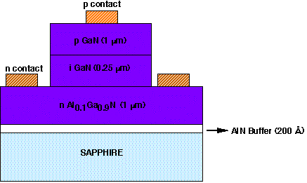
Figure 1. Typical GaN/Al0.1Ga0.9N heterojunction photodiode structure.

Figure 2. Scanning electron micrograph indicating the etched circular mesa structure and the metal contacts.
3. Results and Discussion
Room temperature current vs. voltage measurements on the heterojunction photodiodes, as seen in Figure 3, show extremely low leakage currents under moderate reverse bias and no illumination. The magnitude of the reverse current is measured to be 2-5pA for reverse bias voltages not exceeding -10V. Beyond -15V soft breakdown is observed, with the current magnitude increasing gradually. This increase in current at higher reverse biases is tentatively attributed to defect assisted interband tunneling associated with deep traps in the high field region of the device, i.e. the undoped i-layer.

Figure 3. Current voltage measurements of a typical GaN/Al0.1Ga0.9N p-i-n photodiode at 300K. Note the extremely low leakage current (2-4 pA) for biases greater than -10V.
The photoresponse of the detectors is measured at room temperature at zero bias and under backside illumination through the sapphire substrate. Responsivity results from a detector with an active area of 1.9 ×10⁻³cm2 are shown in Figure 4 (blue curve). Note the logarithmic scale of the vertical axis. The peak response in the UV band from 352nm to 362nm (about 0.2 A/W) is found to be nearly independent of the device area, consistent with elementary considerations (the data shown is from a device with a diameter of 500 μm). The long wavelength fall-off in the responsivity is due to the relatively sharp absorption edge of GaN, which assures that little generation of photocarriers occurs for wavelengths greater than 365nm. Hence, light with wavelength greater than 380nm is rejected by the detector with a ratio of 10−4:1 relative to the peak response near 360nm. The short wavelength fall-off near 350nm is to be attributed to absorption of photons with energies greater than the bandgap of the n-Al0.1Ga0.9N layer. Most of the incident light at these shorter wavelengths is absorbed in the relatively thick n-Al0.1Ga0.9N layer and thus does not reach the active region of the detector. The suppression of the responsivity for short wavelengths is very effective, leading to a responsivity minimum near 340nm which is almost three orders of magnitude less than the peak response.

Figure 4. Measured and calculated spectral responsivity of a typical GaN/Al0.1Ga0.9N p-i-n photodiode on a logarithmic scale.
To understand the performance of the UV-band heterojunction photodiodes more quantitatively we discuss here a simple regional device model. In calculating the responsivity of the device we take into account contributions to the photocurrent that originate from photogenerated holes in the n-Al0.1Ga0.9N layer that diffuse towards the depletion region, from the drift of photogenerated carriers in the depletion regions of the Al0.1Ga0.9N and the GaN, and from the diffusion of electrons in the p-GaN layer diffusing towards the depletion region Reference Van Hove, Hickman, Klaassen, Chow and Ruden[4]. The device is assumed to be illuminated through the n-Al0.1Ga0.9N layer, with reflections at the air/sapphire and the sapphire/detector interfaces taken into account in the model. Structure parameters assumed for the calculations are the design parameters of the MOCVD growth process. The Al0.1Ga0.9N bandgap is calculated based on the empirical relationship given in reference Reference Angerer, Brunner, Freudenberg, Ambacher, Stutzman, Hopler, Metzger, Born, Dollinger, Bergmaier, Karsch and Korner[7]. Additional materials parameters, such as the carrier mobilities, are taken from similarly doped GaN and Al0.1Ga0.9N samples, and the minority carrier lifetimes used are calculated radiative lifetimes.
The absorption coefficient spectrum of GaN without excitonic effects is expressed in parameterized form, with the parameters determined from a fit to the absorption spectrum calculated in reference Reference Wang, Ruden, Kolnik, Oguzman and Brennan[8]. Subsequently, excitonic effects are considered for below and above bandgap absorption Reference Elliott[9]. Using a measured average (A and B) room temperature GaN exciton binding energy of 22meV Reference Liu, Li, Chua, Zhang and Uchida[10] as the appropriate parameter, a large Coulomb enhancement of the above bandgap absorption coefficient is found. The i-GaN region in the photodetector is in the high field region, hence excitonic effects can be assumed to be suppressed here. Similarly, the Coulomb interaction is partially screened in the undepleted regions. Therefore, in our detector model the exciton binding energy is treated as a parameter that assumes different values in different regions but is everywhere smaller than the value found in reference Reference Liu, Li, Chua, Zhang and Uchida[10]. Broadening of the exciton line and of the band edge absorption is taken to be equal to the thermal energy for GaN and somewhat larger for Al0.1Ga0.9N. Evidently, no photocurrent due to hole generation in the n-Al0.1Ga0.9N occurs for photon energies less than the Al0.1Ga0.9N bandgap. On the other hand, for photon energies larger than that bandgap value, the strong absorption in the n-Al0.1Ga0.9N layer effectively suppresses those photocurrent contributions that arise from carrier generation in the GaN part of the device. The three contributions to the total photoresponse are plotted on a logarithmic scale in Figure 5 as a function of the photon wavelength. Figure 4 (purple curve) shows the resultant calculated spectral responsivity of the device. It is apparent that our simple model accounts rather well for the UV-band response in both the magnitude of the maximum responsivity and the band width. However, it is noted that the experimental data displays a slow rise with decreasing wavelength for wavelengths less than 340nm while the model results show a monotonic decrease. This discrepancy is currently under further investigation.
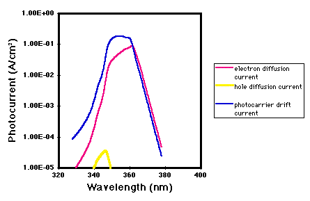
Figure 5. Calculated contributions to the total photocurrent as a function of photon wavelength : Hole diffusion current (essentially negligible) in the n-Al0.1Ga0.9N - yellow curve, electron diffusion current in p-GaN - purple curve and photocarrier drift current in both GaN and AlGaN high field regions - blue curve. The photocurrent components are calculated for an assumed incident intensity of 1W/cm2.
4. Conclusions
We have fabricated and tested GaN/Al0.1Ga0.9N heterojunction p-i-n photodiodes. The detectors have low dark currents of 2-5pA for reverse biases not exceeding -10V, a high UV-band photoresponse in the range between 352nm and 362nm, and strong suppression of the detector response outside that UV band. Near the responsivity peak, the external quantum efficiency of the device is experimentally found to be greater than 80%. This agrees well with the calculated value of 85%. The observed peak responsivity is in satisfactory agreement with the results of a simple model. By increasing the AlN molar fraction in the constituent layers of the device it is possible to shift the response band into the solar blind region of principal interest or into a UV band of specific significance for flame sensing and combustion control.
Acknowledgments
The authors gratefully acknowledge the support of DARPA/ Wright Laboratories and Lockheed Martin under contract # F33615-96-C-1896, supervised by Dr. Paul Schreiber.


