Introduction
Many applications exist for the III-Nitrides in high-power and high-temperature electronics,Reference Aktas, Fan, Mohammed, Botchkarev and Morkoç 1 - Reference McCarthy, Kozodoy, Rodwell, DenBaars and Mishra 3 solar-blind ultraviolet photodetectors,Reference Razeghi and Rogalski 4 and blue and ultraviolet light emitting and laser diodes.Reference Nakamura, Seno, Nagahama, Iwasa, Yamada, Matsushita, Sugimoto and Kiyoku 5 A structure of particular interest for the electronic devices is the AlGaN/GaN two-dimensional electron gas (2DEG) for use in high electron mobility transistors (HEMTs). In this paper, we study in detail the electrical transport properties of a high-mobility AlGaN/GaN 2DEG. Temperature and magnetic field dependent Hall effect measurements are used to study the basic transport properties. Temperature dependent Shubnikov – de Haas (SdH) measurements permitted the extraction of the electron effective mass in GaN. Determination of this constant is important for use in device modeling, but there is considerable scatter in the reported data for the electron effective mass which ranges from 0.18−0.23 m0.Reference Elhamri, Newrock, Mast, Ahoujja, Mitchel, Redwing, Tischler and Flynn 6 - Reference King, Ronning, Davis, Benjamin and Nemanich 9 Two previous reports of the effective mass using SdH measurements for AlGaN/GaN 2DEGs have been made.Reference Elhamri, Newrock, Mast, Ahoujja, Mitchel, Redwing, Tischler and Flynn 6 , Reference Wong, Cai, Li, Wang, Jiang and Chen 7 The SdH measurement for a structure grown on a SiC substrateReference Elhamri, Newrock, Mast, Ahoujja, Mitchel, Redwing, Tischler and Flynn 6 yielded a significantly different result than that measured by other techniques. In this paper, we will use the SdH measurements to estimate the electron effective mass, scattering time, and carrier concentration and compare the results to those obtained by the Hall effect measurements.
Experiment
An AlxGa1-xN/GaN two-dimensional electron gas structure was deposited by molecular beam epitaxy on a 2−3 µm thick GaN layer grown by organometallic vapor phase epitaxy on a sapphire substrate. The AlxGa1−xN was approximately 50 nm thick. The details of the growth have been reported previously.Reference Elsass, Smorchkova, Heying, Haus, Fini, Maranowski, Ibbetson, Keller, Petroff, DenBaars, Mishra and Speck 10
Hall effect measurements were performed over a temperature range of 10 – 300 K and a magnetic field range of 0 – 2 T. Both the Hall effect and the SdH measurements were taken in the four-probe van der Pauw configuration using annealed Ti/Al contacts placed at the four corners of a square.
Measurements of SdH magnetoresistance oscillations were performed using a low ac bias current to avoid electron heating. A magnetic field of 0 − 9 T was used. The temperature was controlled from 1.2 – 4.2 K by immersing the sample in liquid helium and setting the pressure. A calibrated thermometer was then used to measure the temperature.
Results and Discussion
As seen in Fig. 1, the sheet electron concentration and mobility measured by the Hall effect are nearly independent of temperature below about 100 K. This behavior is typical of two dimensional electron gas structures. At 10 K, the electron concentration, nH , was 5.06 × 1012 cm−2, and the Hall mobility, μH , was 1.91 × 10⁴ cmReference Mishra, Wu, Keller, Keller and DenBaars 2 /Vs. The transport scattering time, τc =μHm*/e, where m* is the effective mass and e is the electron charge, was found to be 2.34 ps.

Figure 1. (a) Hall sheet carrier concentration nH as a function of inverse temperature. (b) Hall mobility μ H as a function of temperature.
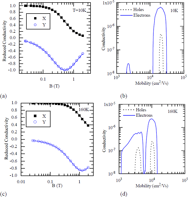
In order to determine if there was any significant parallel conduction at low temperature, magnetic field dependent Hall effect measurements were taken. The data taken at 10 K is plotted in Fig. 2 (a) along with the fit as in the analysis of Kim et al.Reference Kim, Seiler and Tseng 11 The reduced conductivities, X and Y, are σxx and 2σxy respectively divided by the zero field conductivity. When the reduced conductivities are plotted in this manner and only a single electron mobility μ is present, at a magnetic field B=1/μ, X passes through 0.5 and Y peaks with a magnitude of 1. It is clear from this data that there is only one single-carrier conduction path at 10 K. The single carrier fit to this data gives an electron concentration of 5.08 × 1012 cm−2 and a mobility of 1.90 × 10⁴ cmReference Mishra, Wu, Keller, Keller and DenBaars 2 /Vs, in very good agreement with the single magnetic field Hall taken at 0.5 T. The mobility spectrum shown in Fig. 2(b) was obtained using the magnetic field dependent data of Fig. 2(a) processed with software from Lake Shore Cryotronics using the quantitative mobility spectrum analysis technique.Reference Vurgaftman, Meyer, Hoffman, Redfern, Antoszewski, Faraone and Lindemuth 12 This plot also illustrates that there is a single dominant high mobility channel. Fig. 2(c) shows the reduced conductivity at a higher temperature of 160K. From this plot it is apparent that there is more than one conduction path in the sample since Y does not reach −1. A two-carrier fit gives n1=5.0 × 1012 cm−2 , μ1 = 0.82 × 10⁴ cmReference Mishra, Wu, Keller, Keller and DenBaars 2 /Vs, n2 ∼3 × 1013 cm−2 , and μ2 ∼ 2 × 102 cm2/Vs and is plotted as a line. The mobility spectrum also shows a high mobility channel and a lower mobility channel with sigsnificantly lower conductivity. The limited magnetic field range is responsible for reduced certainty in determining the lower mobility. The second lower mobility channel can be interpreted as the bulk-like unintentionally-doped GaN layer which freezes out at low temperatures.

Figure 2. Reduced conductivity as a function of magnetic field (a), and mobility spectrum (b) at 10 K showing that a single-carrier high mobility channel dominates the conduction; and 160 K (c),(d) showing the presence of a second lower mobility channel.

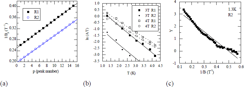
Figure 3. Shubnikov-de Haas oscillations at 1.3 K from two mutually perpendicular sides (a) R1 and (b) R2 of the van der Pauw sample. Notice the attenuation of R1 amplitudes due to a “beating” effect.
The SdH oscillations in the magnetoresistance Rxx(B) were measured at 1.3 K along two mutually perpendicular sides (labeled R1 and R2) of the square van der Pauw sample. A “beating” effect was observed in the amplitude of the R1, as would be expected from two interfering oscillations of slightly different frequencies. Assuming only one subband is occupied and neglecting the contribution of higher harmonics, the oscillatory part Δρxx of the magnetoresistivity can be expressed as:Reference Coleridge, Stoner and Fletcher 13

where χ = 2π 2 kBT / ħωc, ωc = eB/m*, ε = πħ 2 n/m* is the Fermi energy, τq is the quantum scattering time, B is the magnetic field, kB is the Boltzmann constant, T is the absolute temperature, kB is the reduced Plank constant, and n is the sheet electron concentration of the 2DEG. From this equation and the observed magnetic field and temperature dependent magnetoresistance data we will extract the carrier concentration, the effective mass, and the quantum scattering time. This is possible since the magnetoresistance is directly proportional to the magnetoresistivity through a sample geometrical factor.
Since the observed SdH oscillations do not show the presence of higher harmonics, Eq. 6 can be used to obtain the carrier concentration from the frequency of the oscillations in 1/B. Fig. 4(a) shows the inverse magnetic field at which the peak maxima occur. The sheet carrier concentrations for the R1 and R2 oscillations were found to be 4.77 and 4.94 × 1012 cm−2, respectively. The corresponding drift mobilities determined using the observed value of ρo were 2.03 and 1.96 × 104 cm2/Vs. Interestingly, the frequency difference determined from the beating period of the R1 oscillations is found to correspond to an electron concentration difference of about 0.18 × 1012 cm−2. The sheet carrier concentrations obtained from the SdH oscillations are slightly lower than that of the Hall value which may indicate the presence of a very small parallel conduction. The background rise of the R2 oscillations (Fig. 8) indicates field-induced localization of some donor impurities, consistent with small parallel conduction. The small anisotropies observed in the carrier concentration and mobility may result from a slight inhomogeneity in the sample, especially because in the van der Pauw configuration the current paths are not necessarily linear. The observation of the beating effect may also result from this inhomogeneity.

Figure 4. (a) Peak positions in reciprocal magnetic field of SdH oscillations and fit to obtain the carrier concentrations. (b) Fitting for the effective mass for two magnetic field values and two resistivity configurations simultaneously gives m* = 0.215±0.006 m0. (c) Dingle plot for determination of scattering time by fitting the field dependent amplitude.
The effective mass can be extracted by measuring the amplitude of the SdH oscillations as a function of temperature. In Fig. 4(b), the natural logarithm of the amplitude A divided by temperature T is plotted as a function of the temperature. The data was fit simultaneously for two different resistance configurations (labeled R1 and R2) and two different magnetic fields (3 T and 4 T). The value obtained from the fit was 0.215±0.006 m0 which is in good agreement with recently reported values obtained from other techniques such as cyclotron resonance.7−9
Fig. 4(c) is a “Dingle plot” of the R2 oscillation amplitudes (Fig. 8). The quantum relaxation time τq was obtained by fitting the data. Since the amplitudes of R1 oscillations are attenuated by the beating effect, they were not used. The rather poor fit may indicate that some beating is also present in the R2 oscillations. The fit yielded a value of about 0.5 ps for the quantum scattering time, which is significantly lower than the transport scattering time τp of 2.34 ps obtained in the previous section. Note that τq is given by the total scattering rate, whereas τp is weighted by the scattering angle in such a way so as to minimize low-angle scattering. For the 2DEG at the heterointerface, we expect the dominant scattering to be due to long-range potentials associated with donor impurities outside the well which produce predominantly small-angle scattering. A value of τp higher than τq is therefore expected and has often been observed.20
Conclusions
An AlxGa1−xN/GaN two-dimensional electron gas structure with x = 0.13 was deposited by molecular beam epitaxy on a GaN layer grown by organometallic vapor phase epitaxy on a sapphire substrate. Mobility spectrum analysis showed negligible parallel conduction at low temperatures. The sheet carrier concentrations determined from SdH magnetoresistance oscillations were in good agreement with the Hall data. The uncorrected electron effective mass was determined to be 0.215±0.006 based on the temperature dependent amplitude of the SdH oscillations. The quantum lifetime was found to be about one-fifth of the transport lifetime of 2.3 × 10⁻¹² s. We have observed small anisotropies in the electronic properties of the 2DEG at the AlGaN/GaN heterointerface. We currently attribute this anisotropy to a slight inhomogeneity in the sample.
Acknowledgements
The work at UCSB was supported in part by the MRL Central Facilities supported by the NSF under Award No. DMR-9123048. The authors also gratefully acknowledge G. Landis, S. Davidson, A. C. Gossard, J. English, the ONR IMPACT MURI Center at UCSB (C. Wood and J. Zolper contract monitors), AFOSR (G. Witt and D. Johnstone), the Center for Quantized Electronic Structures, HRL Laboratories, the UC-MICRO program, and the NDSEG Fellowship Program.