Introduction
Ohmic contacts with very low contact resistances are essential for improving the performance of optoelectronic devices fabricated on GaN-based materials. For n-type GaN, metallization schemes containing Ti have been very effective in lowering the specific contact resistance (Rc) to less than 10−5 ω-cm2 [Reference Fan, Mohammad, Kim, Aktas, Botchkarev and Morkoc1-Reference Smith, Davis, Liu, Kim and Carpenter3]. In contrast, because of the wide bandgap and the relatively deep acceptor level of the commonly used Mg dopant, it has been very difficult to find ohmic contacts with Rc less than 10−3 ω-cm2 for p-GaN [Reference Liu and Lau4]. So far, only three ohmic metallization and processing schemes on p-GaN have been reported to yield Rc values less than 10−4 ω-cm2. One of these schemes requires a post-metallization anneal of 20 minutes at 800 °C [Reference Suzuki, Kawakami, Arai, Kobayashi, Koide, Uemura, Shibata and Murakami5], while another requires a boiling aqua regia surface etch prior to metal deposition [Reference Kim, Lee, Lee, Shin, Park and Kim6, Reference Kim, Lee, Lee, Park and Kim7]. The third method reduces the resistance of Ni/Au contacts by oxidizing the metallization at 500 °C for 10 minutes and form a thin NiO layer[Reference Ho, Jong, Chiu, Huang, Chen and Shih8]. This work aims at finding a low-resistance ohmic contact on p-GaN which requires less aggressive treatments, thereby making the metallization process more compatible with device processing.
Schubert et al. proposed that the overall hole concentration in p-type GaN can be increased through the generation of valence band edge oscillations in a superlattice[Reference Schubert, Grieshaber and Goepfert9]. This technique improves the activation efficiency of deep acceptors by allowing them to ionize when tunneling occurs from the larger bandgap material into the adjacent material with a narrower bandgap. Significantly enhanced p-type doping efficiency in GaN/AlxGa1−xN short-period superlattices (SL) has been reported recently [Reference Kozodoy, Hansen, DenBaars and Mishra10-Reference Goepfert, Schubert, Osinski and Norris11]. In this paper, we demonstrate excellent ohmic contacts on GaN/AlxGa1−xN SL with a Ti/Pt/Au contact scheme without any aggressive surface treatment and post-metallization anneal. The results are compared to that obtained from the same metallization on p-GaN.
Experimental Details
The superlattice layers used in this study were grown by MBE on sapphire and consisted of 20 periods each of Mg-doped GaN (10 nm) and AlxGa1−xN (10 nm). Samples with two different aluminum concentrations,x=0.1 and 0.2, were investigated. Both samples exhibited a mobility of ∼1 cm2V−1s−1 from room temperature Hall measurements. The reference p-GaN layer used in this study has a 0.3 μm doped layer with a nominal bulk carrier concentration of2.5×1017 cm−3 and a mobility of 9 cm2V−1s−1 as obtained from Hall measurements at room temperature. Contact resistances were determined using the linear transfer length method (TLM). The structures used for the TLM measurements were fabricated by first patterning the p-GaN and SL samples with 100 × 650 μm mesas. The pattern was then transferred into the samples using reactive ion etching, which electrically isolated the mesas. Rectangular pads were then patterned. Prior to transferring the samples into the evaporation chamber, the surfaces were cleaned in O2 plasma, followed by dips in a dilute HCl:DI (1:2) solution. Electron beam evaporation was used to deposit Ti (15 nm) and Pt (50nm), while Au (80nm) was thermally evaporated as the last capping layer. Post-deposition heat treatment was carried out while flowing N2 at 1 atmosphere in a rapid thermal annealing (RTA) system. The contact characteristics were studied using current-voltage (I-V) and four-probe linear TLM techniques at room temperature. For accurate specific contact resistance determination, actual pad distances were determined using scanning electron microscopy (SEM) after metal lift-off.
Results and Discussions
There are several reasons for adopting Ti/Pt/Au metallization for this study. Based on the Schottky-Mott model of metal-semiconductor contacts, the metal-semiconductor barrier height ϕb is related to the work function of the metal ϕm and the electron affinity of a p-type semiconductor χs by ϕb=□(χs □ □ +Eg) − ϕm, provided that there is no Fermi level pinning at the M-S interface. Therefore, metals with high work functions are required to reduce the M-S barrier height for wide band-gap semiconductors such as GaN. Pt, with a ϕm of 5.65 eV, has the highest work function of all metals and is chemically stable. However, experiments have shown that Pt alone suffers from poor adhesion on GaN and therefore, a thin Ti layer is used to improve adhesion as well as getter surface contamination or oxides. The excellent ohmic contacts obtained here for Ti/Pt/Au shows that Ti has been effective in these roles.
Figure 1 shows the current-voltage characteristics of as-deposited Ti/Pt/Au contacts on all three samples. The as-deposited contact is rectifying on the reference p-type GaN. In contrast, due to the enhanced doping efficiencies, the I-V curves for GaN/AlxGa1−xN SL exhibit improved linearity. Figure 1 also reveals that the sample with a higher aluminum mole fraction (x = 0.2) was more ohmic in its I-V characteristics. This is consistent with a calculated carrier concentration of 3×1018 cm−3 for the SL (x = 0.1) versus 5×1018 cm−3 for the other (x = 0.2). An additional mechanism in support of this observation is that the total polarization charge should be higher in the SL with x=0.2 [Reference Kozodoy, Hansen, DenBaars and Mishra10].

Figure 1. Current-voltage characteristics of as-deposited Ti/Pt/Au contacts on p-Type GaN/AlxGa1−xN superlattices (x=0.1 and 0.2)
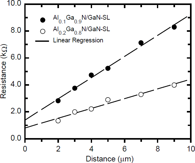
The contact resistivity (ρ c) and specific contact resistance (Rc) were calculated from the measured resistance vs. contact pad spacing data using the linear TLM method. Figure 2 plots the measured resistance vs. pad distance for the as100 deposited Ti/Pt/Au contacts on the two SL samples. Least-square linear regression lines were used to extrapolate the data to the y-axis. The slope of the regression line is a measure of the sheet resistance of the semiconductor. It is clear that the SL with x=0.2 has a smaller slope and therefore a lower sheet resistance, again due to the increased carrier concentration coming from its higher Al mole fraction. ρ c and Rc values can be extracted from the slope of the line,x- and y-intercepts and the pad width. These results are summarized in Table 1. For contacts on semiconductors with NA>1017cm−3, the tunneling process is expected to predominate. In this case, Rc ∞ exp[m(NA)−1/2], where m is a parameter related to the contact barrier height and hole effective mass, and NA, which is the effective carrier concentration. It is clear from this relationship that Rc will be lower for the SL withx = 0.2, and Rc of both SL should be much lower than that of the p-GaN, which is consistent with the results shown in Figure 1 and Table 1.

Figure 2. Measured resistance vs. contact spacing plot for the as-deposited Ti/Pt/Au contacts on p-type GaN/AlxGa1−xN superlattices (x=0.1 and 0.2). Dotted lines are least-square best fits to the different data sets.
Table 1: Summary of results for as-deposited and annealed (at 300 °C for 5 minutes) Ti/Pt/Au contacts on p-type GaN and GaN/AlxGa1−xN superlattices (x=0.1 and 0.2).

Preliminary results on the effectiveness of Ti/Pt/Au contacts on p-type GaN and AlxGa1−xN alloys after annealing are also included in Table 1. Contacts annealed at 300 °C for 5 minutes showed clear improvement. Figure 3 shows an Auger electron spectroscopy (AES) depth profile of the contact metallization after this treatment. Annealing at temperatures higher than 400 °C resulted in rapid degradation of the contacts. The degradation mechanism is currently still under investigation.

Figure 3. AES depth profile of Ti/Pt/Au contacts after annealing for 5 minutes at 300°C. Inset shows AES depth profile of the as-grown p-type GaN/Al0.2Ga0.8N sample.
Conclusions
This study presented the electrical characteristics of Ti/Pt/Au contact on p-type GaN/AlxGa1−xN superlattices. The results indicate effective increase in carrier concentration by using superlattice structures. Ti/Pt/Au has been demonstrated as an effective ohmic metallization scheme on p-type GaN/AlxGa1−xN superlattices, which achieved a specific contact resistance of 1.3×10⁻⁴ Ω-cm2 on GaN/Al0.2Ga0.8N superlattice after annealing for 5 minutes at 300 °C.
Acknowledgements
The materials work at NZ Applied Technologies was supported by BMDO contract N00014-99-M-0277 (Dr. J. Zolper). The work at the University of Illinois was supported by DARPA Grant DAAD19-99-1-0011 (Dr. N. El-Masry and Dr. E. Martinez) and NSF Grant ECS 95-21671.