Hostname: page-component-76fb5796d-vfjqv Total loading time: 0 Render date: 2024-04-25T10:17:15.325Z Has data issue: false hasContentIssue false

Observation of filament formation process of Cu/HfO2/Pt ReRAM structure by hard x-ray photoelectron spectroscopy under bias operation

Published online by Cambridge University Press:  20 January 2012

Takahiro Nagata*
Affiliation:
International Center for Materials Nanoarchitectonics, National Institute for Materials Science, Ibaraki 305-0044, Japan
Masamitsu Haemori
Affiliation:
International Center for Materials Nanoarchitectonics, National Institute for Materials Science, Ibaraki 305-0044, Japan
Yoshiyuki Yamashita
Affiliation:
International Center for Materials Nanoarchitectonics, National Institute for Materials Science, Ibaraki 305-0044, Japan; and NIMS Beamline Station at SPring-8, National Institute for Materials Science, Hyogo 679-5148, Japan
Hideki Yoshikawa
Affiliation:
NIMS Beamline Station at SPring-8, National Institute for Materials Science, Hyogo 679-5148, Japan
Keisuke Kobayashi
Affiliation:
NIMS Beamline Station at SPring-8, National Institute for Materials Science, Hyogo 679-5148, Japan
Toyohiro Chikyow
Affiliation:
International Center for Materials Nanoarchitectonics, National Institute for Materials Science, Ibaraki 305-0044, Japan
*
a)Address all correspondence to this author. e-mail: NAGATA.Takahiro@nims.go.jp
Get access

Abstract

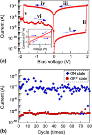
We have demonstrated resistance switching using polycrystalline HfO2 film with a Cu top electrode for nonvolatile memory applications and revealed the Cu diffusion into the HfO2 layer during the filament formation process. Resistive switching was clearly observed in the Cu/HfO2/Pt structure by performing a current–voltage measurement. The current step from a high-resistive state to a low-resistive state was of the order of 103–104 Ω, which provided a sufficient on/off ratio for use as a switching device. The filament formation process was investigated by employing hard x-ray photoelectron spectroscopy under bias operation. The application of a bias to the structure reduced the Cu2O state at the interface and the intensity ratio of Cu 2p3/2/Hf 3d5/2, providing evidence of Cu2O reduction and Cu diffusion into the HfO2 layer. These results also provide evidence that the resistance switching of the Cu/HfO2/Pt structure originates in a solid electrolyte (nanoionics model) containing Cu ions.

Type
Invited Feature Paper
Copyright
Copyright © Materials Research Society 2012

Access options

Get access to the full version of this content by using one of the access options below. (Log in options will check for institutional or personal access. Content may require purchase if you do not have access.)

References

REFERENCES

1.Waser, R.: Resistive non-volatile memory devices. Microelectron. Eng. 86, 1925 (2009).CrossRefGoogle Scholar
2.Karg, S.F., Meijer, G.I., Bednorz, J.G., Rettner, C.T., Schtorr, A.G., Joseph, E.A., Lam, C.H., Janousch, M., Staub, U., La Mattina, F., Alvarado, S.F., Widmer, D., Stutz, R., Drechsler, U., and Caimi, D.: Transition-metal-oxide-based resistance-change memories. IBM J. Res. Dev. 52, 481 (2008).Google Scholar
3.Pagnia, H. and Sotnik, N.: Bistable switching in electroformed metal–insulator–metal devices. Phys. Status Solidi A 108, 11 (1988).Google Scholar
4.Chudnovskii, F.A., Odynets, L.L., Pergament, A.L., and Stefanovich, G.B.: Electroforming and switching in oxides of transition metals: The role of metal–insulator transition in the switching mechanism. J. Solid State Chem. 122, 95 (1996).CrossRefGoogle Scholar
5.Asamitsu, A., Tomioka, Y., Kuwahara, H., and Tokura, Y.: Current switching of resistive states in magnetoresistive manganites. Nature 388, 50 (1997).Google Scholar
6.Fors, R., Khartsev, S.I., and Grishin, A.M.: Giant resistance switching in metal-insulator-manganite junctions: Evidence for Mott transition. Phys. Rev. B 71, 045305 (2005).CrossRefGoogle Scholar
7.Kim, D.S., Kim, Y.H., Lee, C.E., and Kim, Y.T.: Colossal electroresistance mechanism in a Au/Pr0.7Ca0.3MnO3/Pt sandwich structure: Evidence for a Mott transition. Phys. Rev. B 74, 174430 (2006).CrossRefGoogle Scholar
8.Meijer, G.I., Staub, U., Janousch, M., Johnson, S.L., Delley, B., and Neisius, T.: Valence states of Cr and the insulator-to-metal transition in Cr-doped SrTiO3. Phys. Rev. B 72, 155102 (2005).CrossRefGoogle Scholar
9.Waser, R. and Aono, M.: Nanoionics-based resistive switching memories. Nat. Mater. 6, 833 (2007).CrossRefGoogle ScholarPubMed
10.Sakamoto, T., Sunamura, H., Kawaura, H., Hasegawa, T., Nakayama, T., and Aono, M.: Nanometer-scale switches using copper sulfide. Appl. Phys. Lett. 82, 3032 (2003).Google Scholar
11.Banno, N., Sakamoto, T., Hasegawa, T., Terabe, K., and Aono, M.: Effect of ion diffusion on switching voltage of solid-electrolyte nanometer switch. Jpn. J. Appl. Phys. 46, 3666 (2006).CrossRefGoogle Scholar
12.Terabe, K., Hasegawa, T., Nakayama, T., and Aono, M.: Quantized conductance atomic switch. Nature 433, 47 (2005).CrossRefGoogle ScholarPubMed
13.Kozicki, M.N., Park, M., and Mitkova, M.: Nanoscale memory elements based on solid-state electrolytes. IEEE Trans. Nanotechnol. 4, 331 (2005).Google Scholar
14.Kim, Y-M. and Lee, J-S.: Reproducible resistance switching characteristics of hafnium oxide-based nonvolatile memory devices. J. Appl. Phys. 104, 114115 (2008).Google Scholar
15.Sakamoto, T., Lister, K., Banno, N., Hasegawa, T., Terabe, K., and Aono, M.: Electronic transport in Ta2O5 resistive switch. Appl. Phys. Lett. 91, 92110 (2007).Google Scholar
16.Lee, S., Kim, W-G., Rhee, S-W., and Yong, K.: Resistance switching behaviors of hafnium oxide films grown by MOCVD for nonvolatile memory applications. J. Electrochem. Soc. 155, H92 (2008).CrossRefGoogle Scholar
17.Gibbons, J.F. and Beadle, W.E.: Switching properties of thin NiO films. Solid-State Electron. 7, 785 (1964).CrossRefGoogle Scholar
18.Tsuchiya, T., Oyama, Y., Miyoshi, S., and Yamaguchi, S.: Nonstoichiometry-induced carrier modification in gapless type atomic switch device using Cu2S Mixed Conductor. Appl. Phys. Express 2, 055002 (2009).CrossRefGoogle Scholar
19.Haemori, M., Nagata, T., and Chikyow, T.: Impact of Cu electrode on switching behavior in a Cu/HfO2/Pt structure and resultant Cu ion diffusion. Appl. Phys. Express 2, 061401 (2009).CrossRefGoogle Scholar
20.Wilk, G.D. and Wallace, R.M.: Electrical properties of hafnium silicate gate dielectrics deposited directly on silicon. Appl. Phys. Lett. 74, 2854 (1999).Google Scholar
21.Robertson, J.: High-dielectric constant gate oxides for metal oxide Si transistors. Rep. Prog. Phys. 69, 327 (2006).Google Scholar
22.Yang, J.J., Miao, F., Pickett, M.D., Ohlberg, D.A.A., Stewart, D.R., Lau, C.N., and Williams, R.S.: The mechanism of electroforming of metal oxide memristive switches. Nanotechnology 20, 215201 (2009).CrossRefGoogle Scholar
23.Yoshida, C., Kinoshita, K., Yamasaki, T., and Sugiyama, Y.: Direct observation of oxygen movement during resistance switching in NiO/Pt film. Appl. Phys. Lett. 93, 042106 (2008).CrossRefGoogle Scholar
24.Shima, H., Takano, F., Muramatsu, H., Yamazaki, M., Akinaga, H., and Kogure, A.: Local chemical state change in Co–O resistance random-access memory. Phys. Status Solidi RRL. 2, 99 (2008).Google Scholar
25.Yamashita, Y., Ohmori, K., Ueda, S., Yoshikawa, H., Chikyow, T., and Kobayashi, K.: Bias-voltage application in hard x-ray photoelectron spectroscopy for characterization of advanced materials. e-J. Surf. Sci. Nanotechnol. 8, 81 (2010).CrossRefGoogle Scholar
26.Nagata, T., Haemori, M., Yamashita, Y., Iwashita, Y., Yoshikawa, H., Kobayashi, K., and Chikyow, T.: Oxygen migration at Pt/HfO2/Pt interface under bias operation. Appl. Phys. Lett. 97, 082902 (2010).CrossRefGoogle Scholar
27.Tsuruoka, T., Terabe, K., Hasegawa, T., and Aono, M.: Forming and switching mechanisms of a cation-migration-based oxide resistive memory. Nanotechnology 21, 425205 (2010).CrossRefGoogle ScholarPubMed
28.Ueda, S., Tanaka, M., Yoshikawa, H., Yamashita, Y., Matsushita, Y., Kobayashi, K., Katsuya, Y., and Ishimaru, S.: Present status of the NIMS contract beamline BL15XU at SPring-8. AIP Conf. Proc. 1234, 403 (2010).CrossRefGoogle Scholar
29.Doniach, S. and Šunjić, M.: Many-electron singularity in x-ray photoemission and x-ray line spectra from metals. J. Phys. Chem. 3, 285 (1970).Google Scholar
30.Shirley, D.A.: High-resolution x-ray photoemission spectrum of the valence bands of gold. Phys. Rev. B. 5, 4709 (1972).Google Scholar
31.Tanuma, S., Powell, C.J., and Penn, D.R.: Calculations of electron inelastic mean free paths for 31 materials. Surf. Interface Anal. 11, 577 (1988).Google Scholar
32.Powell, C.J., Jablonski, A., Tilinin, I.S., Tanuma, S., and Penne, D.R.: Surface sensitivity of Auger-electron spectroscopy and x-ray photoelectron spectroscopy. J. Electron. Spectrosc. Relat. Phenom. 9899, 1 (1999).CrossRefGoogle Scholar
33.Tanuma, S.: Electron scattering effect on surface electron spectroscopies. J. Surf. Sci. Soc. Jpn. 27, 657 (2006).CrossRefGoogle Scholar
34.Yang, J.J., Pickett, M.D., Li, X., Ohlberg, D.A.A., Stewart, D.R., and Williams, R. S.: Memoristive switching mechanism for metal/oxide/metal nanodevices. Nat. Nanotechnol. 3, 429 (2008).Google Scholar
35.Schroeder, H. and Jeong, D.S.: Resistive switching in a Pt/TiO2/Pt thin film stack—a candidate for a non-volatile ReRAM. Microelectron. Eng. 84, 1982 (2007).CrossRefGoogle Scholar
36.Poulston, S., Parlett, P.M., Stone, P., and Bowker, M.: Surface oxidation and reduction of CuO and Cu2O studied using XPS and XAES. Surf. Interface Anal. 24, 811 (1996).3.0.CO;2-Z>CrossRefGoogle Scholar
37.Galtayrise, A. and Bonnelle, J-P.: XPS and ISS studies on the interaction of H2S with polycrystalline Cu, Cu2O and CuO surfaces. Surf. Interface Anal. 23, 171 (1995).CrossRefGoogle Scholar
38.Rhodin, T.N. Jr.: Low temperature oxidation of copper. I. Physical mechanism. J. Am. Chem. Soc. 72, 5102 (1950).CrossRefGoogle Scholar
39.Iijima, J., Lim, J-W., Hong, S-H., Suzuki, S., Mimura, K., and Isshiki, M.: Native oxidation of ultra high purity Cu bulk and thin films. Appl. Surf. Sci. 253, 2825 (2006).CrossRefGoogle Scholar
40.Himpsel, F.J., McFeely, F.R., Taleb-Ibrahimi, A., Yarmoff, J.A., and Hollinger, G.: Microscopic structure of the SiO2/Si interface. Phys. Rev. B: Condens. Matter 38, 6084 (1988).Google Scholar
41.Kobayashi, K., Yabashi, M., Takata, Y., Tokushima, T., Shin, S., Tamasaku, K., Miwa, D., Ishikawa, T., Nohira, H., Hattori, T., Sugita, Y., Nakatsuka, O., Sakai, A., and Zaima, S.: High resolution-high energy x-ray photoelectron spectroscopy using third-generation synchrotron radiation source, and its application to Si-high k insulator systems. Appl. Phys. Lett. 83, 1005 (2003).CrossRefGoogle Scholar
42.Barreca, D., Milanov, A., Fischer, R.A., Devi, A., and Tondello, E.: Hafnium oxide thin film grown by ALD: An XPS study. Surf. Sci. Spectra 14, 34 (2007).Google Scholar
43.Paàl, Z., Muhler, M., and Schlögl, R.: Platinum black by XPS. Surf. Sci. Spectra 4, 119 (1996).Google Scholar
44.Jung, M-C., Kim, H-D., Han, M., Jo, W., and Kim, D.C.: X-ray photoelectron spectroscopy study of Pt-oxide thin films deposited by reactive sputtering using O2/Ar gas mixtures. Jpn. J. Appl. Phys. 38, 4872 (1999).Google Scholar
45.Matolín, V., Cabala, M., Matolínová, I., Škoda, M., Václavů, M., Prince, K.C., Skála, T., Mori, T., Yoshikawa, H., Yamashita, Y., Ueda, S., and Kobayashi, K.: Pt and Sn doped sputtered CeO2 electrodes for fuel cell application. Fuel Cells (Weinh.) 10, 139 (2010).CrossRefGoogle Scholar
46.Bard, A.J. and Faulkner, L.R.: Electrochemical Methods. Fundamentals and Applications, 2nd ed. (John Wiley & Sons Inc, New York, 2001), pp. 808809.Google Scholar
47.Yoshitake, M., Aparna, Y-R., and Yoshihara, K.: General rule for predicting surface segregation of substrate metal on film surface. J. Vac. Sci. Technol. A 19, 1432 (2001).CrossRefGoogle Scholar
48.Takeuchi, H., Ha, D., and King, T-J.: Observation of bulk HfO2 defects by spectroscopic ellipsometry. J. Vac. Sci. Technol. A 22, 1337 (2004).Google Scholar
49.Ohmori, K., Ahmet, P., Yoshitake, M., Chikyow, T., Shiraishi, K., Yamabe, K., Watanabe, H., Akasaka, Y., Nara, Y., Chang, K-S., Green, M.L., and Yamada, K.: Influences of annealing in reducing and oxidizing ambients on flatband voltage properties of HfO2 gate stack structures. J. Appl. Phys. 101, 084118 (2007).CrossRefGoogle Scholar