Introduction
Focused ion beam instruments (FIBs) are extremely flexible systems useful for fabricating a wide range of devices and specimens [Reference Giannuzzi and Stevie1–Reference Kim5]. A common FIB application in our facility is to fabricate arrays of isolated structures in thin metal and/or ceramic films that have been deposited on large flat glass substrates [Reference Escobedo6, Reference Brolo7]. Typically many structures, each with features on the order of 100 nm, are fabricated over an area as large as 200 mm2 in the center of the substrate. Each structure requires a fabrication resolution near the limit of the instrument and must be fabricated at high magnification; only one fabrication can be made at a time. In addition, the entire region surrounding the fabrications must be pristine; the cuts must be made without checking focus at the fabrication point.
During previous tests with these flat plane specimens, it was discovered that when the fabrication point was moved away from the focus point, fabrication quality degraded. It was determined that the ion beam became defocused away from the initial focus point; therefore, the specimen was not perfectly perpendicular to the beam. This phenomenon was attributed to a tilt of the flat specimen. This situation was caused by a combination of imperfections in the manufacturing of the sample holder, the attachment of the sample stub to the holder, and the mounting of the specimen to the sample stub.
To counteract this problem, the user would need to refocus the beam adjacent to each fabrication point. However, in addition to being time-consuming, the act of focusing the beam damages the delicate thin film. These specimens are fabricated for experiments that illuminate the arrays of holes with different wavelengths of light, and, because of the nature of the experiments, thin-film damage that allows light leaks near the fabrication locations is not acceptable.
This article presents a method to overcome this difficulty by computing the correct voltage for the electrostatic focusing lens as a function of the {X, Y} position on the surface of the specimen. This allows high-resolution features to be fabricated at arbitrary locations on a large flat sample without having to refocus at each location.
Methods and Materials
A 25.4 mm × 25.4 mm (1 inch × 1 inch) flat plane substrate was prepared to test this method. A Bio Nuclear Diagnostics microscope slide (1 inch × 3 inches) was cut to obtain a 1 inch × 1 inch square, sonicated for 5 minutes in each of a series of solvents (acetone, ethanol, methanol, and isopropanol), and blow-dried with nitrogen. An Angstrom Engineering electron beam deposition system was used to deposit a 2 nm thick titanium bonding film followed by a 100 nm thick gold film. The specimen was attached to an SEM pin stub with beryllium-copper clamps, and a Sharpie™ fine point black marker was used to place 300 µm diameter reference points at three locations on the gold film just inside the 15 mm × 15 mm working area of the Hitachi FB-2100 FIB, as illustrated in Figure 1. The FB-2100 was then used to fabricate identifying marks (letters A, B, C) on the Sharpie dots, an example of which is shown in Figure 2. These dots serve as reference points to complete the orientation of the specimen plane and as fiducial marks for locating the fabrications in a Hitachi S-4800 SEM. To summarize the method, a reference fabrication was made at A, and two sets of fabrications were made at locations B and C: first without focus correction to demonstrate the fabrication issues caused by specimen tilt and then with focus correction to demonstrate the improvement.

Figure 1 Fabrication locations in a 15 mm × 15 mm area of the specimen. Sharpie™ dots are indicated by open circles marked A, B, and C. Fabrication locations are solid dots marked 1 through 5.
Figure 2 Sharpie™ dot at location A with identifying mark produced with the FIB.
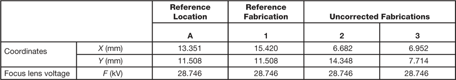
First the FB-2100 was focused and aligned at reference location A. The X and Y coordinates and focus lens voltage F for the reference location A are shown in Table 1. Without any further focus correction, three fabrications were made: fabrication location 1 adjacent to point A, location 2 adjacent to point B, and location 3 adjacent to point C, as illustrated in Figure 1.
Table 1 Coordinates and ion lens focus voltages for the uncorrected-fabrication test. Reference fabrication 1 was made directly adjacent to the focus point at A. Points 2 and 3 are the locations of fabrications made without focus correction.
Each fabrication was a 30 × 30 array of 200 nm diameter holes spaced 450 nm apart, produced using a 40 kV beam with 13.5 pA current, 10 μs/pixel dwell time, 50 raster passes, and 10,000 times magnification. These fabrications were at distances of 0.069 mm, 9.122 mm, and 9.136 mm, respectively, from the focus point at A. They were used to confirm that the sample plane was tilted and for comparison with the focus-corrected fabrications to follow.
If the focus lens voltage F is assumed to be proportional (or inversely proportional) to working distance Z and the specimen is assumed to be perfectly flat, three points on the surface of the specimen may be used to define a plane in {X, Y, F}. Because the specimen was an optically flat microscope slide, only the linearity of F versus Z needed to be tested.
In an experiment conducted separately, but with the same specimen and beam parameters used for the present fabrications, focus lens voltage F was recorded as a function of working distance Z. The relationship is shown in Figure 3 along with computed linear fit line. The correlation coefficient for linear fit is nearly equal to -1, which shows that F and Z can be considered inversely proportional.
Figure 3 Measured focus lens voltage F as a function of working distance Z, showing the linear fit line and the values of the slope and correlation coefficient.
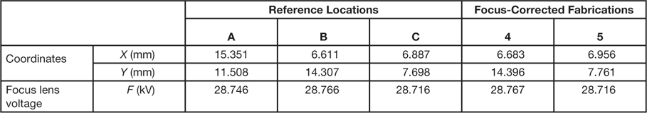
To demonstrate the lens focus correction method, the FB-2100 was focused on two additional reference points, B and C, illustrated in Figure 1, and the X and Y coordinates and focus lens voltage F were recorded for each point, as shown in Table 2. These values were used in the method described below to compute the corrected focus lens voltages for fabrications at locations 4 and 5, adjacent to points B and C, respectively.
Table 2 Coordinates and focus lens voltages for the corrected-fabrication test. Reference locations A, B, and C were used to compute the focus lens voltage values used for fabrications at points 4 and 5.
Correction Equations
Knowing that the focus lens voltage F is inversely proportional to working distance Z, the equation of the plane {X,Y, F} is
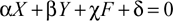 \[$\alpha X\, + \,\beta Y\, + \,\chi F\, + \,\delta \, = \,0$\]
Using the three points A, B and C (defined with coordinates {A X,A Y,A F}, {B X,B Y,B F}, {C X,C Y,C F}), the plane equation coefficients α, β, χ and δ are computed as:
 \[$\alpha \, = \,A_{{\rm Y}} \left( {B_{{\rm F}} \,{\rm - }\,C_{{\rm F}} } \right)\, + \,B_{{\rm Y}} \left( {C_{{\rm F}} \,{\rm - }\,A_{{\rm F}} } \right)\, + \,C_{{\rm Y}} \left( {A_{{\rm F}} \,{\rm - }\,B_{{\rm F}} } \right)$\]\[$\eqalign{ & \beta \, = \,A_{{\rm F}} \left( {B_{{\rm X}} \,{\rm - }\,C_{{\rm X}} } \right)\, + \,B_{{\rm F}} \left( {C_{{\rm X}} \,{\rm - }\,A_{{\rm X}} } \right)\, + \,C_{{\rm F}} \left( {A_{{\rm X}} \,{\rm - }\,B_{{\rm X}} } \right) \cr & \chi \, = \,A_{{\rm X}} \left( {B_{{\rm Y}} \,{\rm - }\,C_{{\rm Y}} } \right)\, + \,B_{{\rm X}} \left( {C_{{\rm Y}} \,{\rm - }\,A_{{\rm Y}} } \right)\, + \,C_{{\rm X}} \left( {A_{{\rm Y}} \,{\rm - }\,B_{{\rm Y}} } \right) \cr & \delta \, = \,{\rm - }A_{{\rm X}} \left( {C_{{\rm F}} B_{{\rm X}} \,{\rm - }\,C_{{\rm Y}} B_{{\rm F}} } \right)\,{\rm - }\,B_{{\rm X}} \left( {C_{{\rm Y}} A_{{\rm F}} \,{\rm - }\,C_{{\rm F}} A_{{\rm Y}} } \right)\,{\rm - }\,C_{{\rm X}} \left( {A_{{\rm Y}} B_{{\rm F}} \,{\rm - }\,A_{{\rm F}} B_{{\rm Y}} } \right) \cr} $\]
Then the lens focus voltage F P can be computed for any point P {P X,P Y} as:
 \[$F_{P} \left( {P_{X}, P_{Y} } \right)\, = \,{\rm - }(\alpha P_{X} \, + \,\beta P_{Y} \, + \,\delta )/\chi $\]
The point P is represented in this plane as {P X,P Y,F P}.
Using this definition of the plane, two more fabrications were made using the same beam conditions but with corrected focus lens voltages: at location 4 and 5 directly adjacent to reference point B and C, respectively (as indicated in Figure 1 and Table 2). These focus-corrected locations were at a distances of 9.136 mm and 9.193 mm from the initial focus point A, respectively. For each of these two fabrications, the focus lens voltage F 4 and F 5 was computed using the X and Y coordinates of points 4 and 5 and Equation 1.
Results
The specimen was re-mounted on a large stub with colloidal carbon paint, loaded in a Hitachi S-4800 FESEM, and imaged with 2.0 mm working distance, 2 keV electrons, and 20 μA emission current with the upper through-the-lens (TTL) detector.
Figure 4 shows the first fabrication at location 1, which was used as a reference. This is the ideal focus lens condition. It was fabricated 0.069 mm from the focus point at reference point A. This fabrication shows what the structure should look like when it is fabricated directly adjacent to the focus point.
Figure 4 Portion of a reference fabrication at location 1 produced adjacent to reference location A. The distance from focus point to fabrication was 0.069 mm.
The results for the two non-corrected fabrications at locations 2 and 3 are shown in Figures 5 and 6. These locations are shown on the layout diagram in Figure 1.
Figure 5 Portion of an uncorrected fabrication at location 2, adjacent to point B, located 9.122 mm from the focus point at A.
Figure 6 Portion of an uncorrected fabrication at location 3, adjacent to point C, located 9.216 mm from the focus point A.
The two computationally focus-corrected fabrications are shown in Figures 7 and 8. The structure in Figure 7 (location 4) was fabricated directly adjacent to the uncorrected fabrication in Figure 5 (location 2), and the fabrication in Figure 8 (location 5) was fabricated directly adjacent to the uncorrected fabrication in Figure 6 (location 3).
Figure 7 Portion of a focus-corrected fabrication at location 4, adjacent to point B, located 9.136 mm from the focus point at A.
Figure 8 Portion of a focus-corrected fabrication at location 5, adjacent to point C, located 9.193 mm from the focus point at A.
Discussion
Although the reference fabrication in Figure 4 was made with the ideal focus condition and shows no defocus artifacts, the fabrication is not perfect. The first imperfection is that the holes are not perfectly round. The holes only approximate roundness because the fabrication resolution at the holes was limited by the size of the holes relative to the overall size of the bitmap. The overall array size was 13.25 μm × 13.25 μm (a requirement of the client’s experiment), which meant that the array had to be fabricated at a relatively low magnification (10k) so that the entire structure could be fabricated at once. As a result, there are only 778 pixels (measured with ImageJ) representing each hole in the bitmap; this makes the hole edges stepped and/or out of round. The second imperfection is that there are regions between the holes along the horizontal rows where the gold grains appear blurred. The first approach to analyze this was to take SEM images with different rotations and beam conditions to ensure that it was a FIB artifact rather than an imaging artifact. This work showed that the blurred regions were a FIB artifact. It was realized that the FIB’s beam was programmed to raster horizontally for these fabrications. A fabrication was repeated with vertical raster, and the resulting film damage was instead along the vertical rows of holes. Along the raster direction, the film between the holes was heated by adjacent fabrication points causing the grains to deform.
An examination of Figures 5 and 6 shows that if the uncorrected fabrications are sufficiently distant from the focus point at A, the quality of the fabrication degrades. This confirms that the sample was not perpendicular to the beam and that a focus correction would be required for proper fabrication. Corroborating this, the focus lens voltage used for uncorrected fabrications 2 and 3 shown in Figures 5 and 6 (28.746 kV) was different from the measured focus lens voltages at point B (28.766 kV) and C (28.716 kV), as shown in Table 2.
Because the equation of the sample plane is known, it is possible to compute how far out of focus the uncorrected fabrications 2 and 3 were. Using Equation 1 together with the reference locations A, B, and C from Table 2 and the location coordinates of the uncorrected fabrications from Table 1, the corrected focus lens voltage for location 2 would have been 28.766 kV and for location 3 would have been 28.716 kV. Thus, the uncorrected focus lens voltage at point 2 was out of focus by -0.02 kV and at point 3 by +0.03 kV. Using the slope of the linear fit in Figure 3, it is determined that location 2 was fabricated with a beam that was 35 μm overfocused, and location 3 was fabricated with a beam that was 53 μm underfocused.
In the case of the focus corrected fabrications, a visual comparison of the reference fabrication (Figure 4) with the focus-corrected fabrications 4 and 5 (Figures 7 and 8) confirms that the corrected fabrications are of equal quality to the initial reference fabrication. In addition, the computed focus lens voltages used for corrected fabrications 4 and 5 (28.767 kV and 28.716 kV) were practically equal to the measured focus lens voltages at adjacent locations B (28.766 kV) and C (28.716 kV), respectively. From these results it appears that the method is effective in compensating for flat surfaces that are not perpendicular to the beam.
Conclusions
A method to allow nanometer-resolution ion beam fabrication at arbitrary locations on a large flat plane sample has been demonstrated. Flat plane sample tilt can be corrected by defining the sample surface as a flat plane in {X, Y, F(X,Y)} and computing a function F(X,Y) for the focus lens voltage F. Structures at any arbitrary position {X,Y} can then be fabricated without having to damage the sample when checking focus at each location. This greatly reduces the effort required to fabricate nanoscale structures over a large area with a FIB system and increases the instrument’s utility by allowing large arrays of structures to be fabricated without damaging the specimen.