


Introduction
Various advanced wireless communication technologies have already emerged during the past few decades, which, have significantly influenced and benefited the human life in different way. Despite of high data rate, ultra-wideband (UWB) system consumes low power compared with the other narrow band systems, resulting in not causing undesired interference to the existing communication systems. However, strong signals from pre-existing narrow bands such as IEEE 802.16 WiMAX (operating at 3.3–3.8 GHz), IEEE 802.11a WLAN (covering 5.15–5.825 GHz band), and HIPERLAN (5.15–5.47 GHz) may degrade the UWB system's performance due to strong interference. Although this problem can be minimized by the use of spatial filters, it will elevate the cost and system complexity. Therefore, it is necessary to design UWB antennas with band-notch function.
To attain band-notch characteristics, several techniques have been proposed. These techniques include insertion of different types of slots in the patch or ground plane [Reference Yadav, Sethi and Khanna1–Reference Cho, Kim, Choi, Lee and Park3], etching of slot/s on the feed line [Reference Mao and Chu4], addition of parasitic strips and split rings near the patch, feed line, or ground plane [Reference Liu, Yin, Liu, Wang and Xu5–Reference Siddiqui, Saha and Antar8] and printing of different types of resonators on/beneath the radiating patch [Reference Yadav, Abegaonkar, Koul, Tiwari and Bhatnagar9, Reference Lui, Cheng and Zhu10]. For example in [Reference Yadav, Sethi and Khanna1], three rectangular slots have been cut on the patch to create dual notch band at WLAN and X-band. Though it notches X-band used in satellite communication, it fails to filter out the popular WiMAX band. To achieve multiple band-notch characteristics, in [Reference Rehman and Alkanhal2] four meander-shaped defected ground structured slots have been etched in the ground plane. This design shows sharp band rejection characteristics, but it possesses a large volumetric dimension of 8624.0 mm3. In [Reference Mao and Chu4], dual band-notch characteristics at 3.6/5.5 GHz with UWB operating band is achieved by etching an S-shaped slot on the feed line. Despite of fairly compact size (36 mm × 30 mm), the reported antenna's notch bands are larger than the required notch bands for WiMAX and WLAN which may degrade the quality of the received signal. In order to generate dual notch bands at 3.3–3.7 and 5.15–5.8 GHz, a pair of bended dual L-shaped parasitic branches is added to the slotted ground plane of the antenna presented in [Reference Liu, Yin, Liu, Wang and Xu5]. But this design is characterized with irregular structure and relatively large size. In [Reference Azim, Islam and Mobashsher6], to create a notch band at 3.5 GHz, an angle-shaped parasitic slit is etched in the front of the substrate along with the patch, while to attain another notch band at 5.5 GHz, a pair of symmetrical slits is placed within the slot of the ground plane. In [Reference Jiang and Che7], to realize a notch band at WiMAX, an inverted T-shaped stub is embedded in the square slot of the radiating patch, while a pair of rotated U-shaped parasitic strips is imprinted beside the feed line to generate another notch band at WLAN. Though the design is compact, the achieved bandwidths (BWs) of the notch bands are larger than the required BW. To create dual notch band at around 5.34 and 7.95 GHz, two pairs of square-shaped split-ring resonators are printed on the back side of the antenna reported in [Reference Siddiqui, Saha and Antar8]. However, the antenna size is big and it does not notch the 3.5 GHz WiMAX band. To achieve stop band characteristics at WLAN (5–5.4 GHz) and ITU band (7.8–8.4 GHz) in [Reference Yadav, Abegaonkar, Koul, Tiwari and Bhatnagar9], one inverted U-shaped and one iron-shaped parasitic resonator are etched on the back side of the radiating patch. The layout of this antenna is fairly compact but it notches the WLAN band partially. Uses of metamaterials and electromagnetic bandgap structures have also been reported to design band-notch UWB antennas [Reference Mansouri, Arezomand, Heydari and Zarrabi11, Reference Li, Zhai, Li and Liang12]. Although many of the above mentioned antennas exhibit desired band-notch characteristics, they are featured with disadvantages like complex structure, large volumetric size, and strong coupling between the band-notch elements. Moreover, many reported band-notch UWB antennas use band-notch elements that are simultaneously imprinted on both sides of the substrate which may create fabrication difficulties. Therefore, it is quite challenging to design band-notch UWB antenna with compact volumetric size.
A compact planar UWB antenna with a size of 30 mm × 22 mm × 1.6 mm is presented in the paper. To generate two notch bands, a pair of parasitic resonator is placed beneath the patch without changing the size and shape of the radiator and ground plane. The presented antenna covers the frequency spectrum ranging from 2.98 to 12 GHz thereby maintain a VSWR ≤2. Moreover, the designed antenna exhibits two notch bands at 3.5 and 5.45 GHz, achieved an average gain of 3.95 dBi, and demonstrates stable radiation patterns throughout the operating BW except at notch bands.
Design of the proposed antenna
Figure 1 presents the design of the proposed microstrip planar UWB antenna which is composed of almost square-shaped radiating patch with partial ground plane. The microstrip patch of the presented antenna is etched on one side of a standard FR4 dielectric substrate. The substrate material has a compact dimension of W × L with a thickness of 1.6 mm, a relative permittivity of 4.6, and a tanδ of 0.02. To feed the antenna, a microstrip line of size w f × l f is printed on the same side of the substrate along with the patch. To enhance the operating BW, the partial ground plane is modified by inserting triangular-shaped slots and is printed on the other side of the FR4 material. An SMA connector is attached to the base of the 50 Ω microstrip feed line. The change in the ground plane shape and dimension causes the change in capacitance and inductance of the input impedance resulting in a change in operating BW. The slots in the top edge of the partial ground plane alter the distances between the patch and the ground plane and influence the coupling between them and consequently the BW is enhanced. It is found that insertion of triangular-shaped slots on the top edge of the partial ground plane enhanced the operating BW by 43.6% [Reference Azim, Islam and Misran13]. The parameters of the presented antenna structure without resonating elements are as follows: W = 30 mm, L = 22 mm, W P = 14.5 mm, L P = 14.75 mm, L G = 7.5 mm, w f = 3 mm, l f = 7.25 mm.
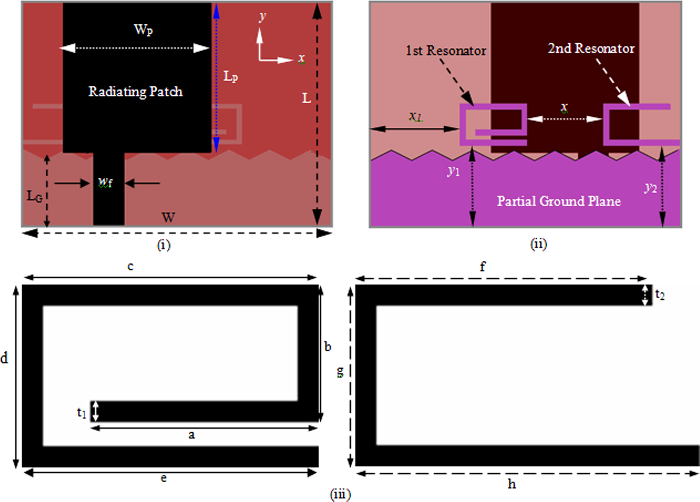
Fig. 1. Layout of the presented antenna structure (i) top view, (ii) bottom view, and (iii) resonators.
To produce two notch bands with an aim to minimize the electromagnetic interferences between WiMAX, WLAN, and UWB systems, a pair of parasitic resonators has been printed beneath the patch as depicted in Fig. 1(ii). To attain a notch band at WiMAX band, first resonator of total length L 1 (=a + b + c + d + e) is printed symmetrically at a distance x 1 mm from the left edge of the substrate. The second notch band at WLAN can be obtained by etching another resonating element of length L 2 (=f + g + h) at a distance x mm from the first one. The first and second resonators are, respectively, at y 1 and y 2 mm away from the top edge of the slotted ground plane. The total length of the each resonator is equal to about half of the guided wavelength and is given by
 $$L = \displaystyle{{\lambda _g} \over 2} = \displaystyle{{\lambda _0} \over {2\sqrt {\varepsilon _r + 1}}} = \displaystyle{c \over {2f_{notch}\sqrt {\varepsilon _r + 1}}}, $$
where λ 0 is the free space wavelength, c is the velocity of light, ε r is the relative dielectric constant of the substrate, and f notch is the center frequency of the respective notch bands. The detail dimensions of the different parameters of the resonators are depicted in Fig. 1(iii).
The current distributions on the surface of the presented antenna at 3.5 GHz (notch band), 4.28 GHz (pass band), 5.45 GHz (notch band), and 8.0 GHz (pass band) are displayed in Figs 2(a)–2(d) correspondingly. In the plot, the currents are strongly concentrated as it approaches the areas marked red and distribution becomes denser. Figure 2(a) presents the current distribution at first notch band of 3.5 GHz where it is seen that most of the surface current concentrated around the first resonator while the currents in the rest of the antenna are very weak. The current distribution at second notch band of 5.45 GHz depicted in Fig. 2(c) indicates that the surface current at the second resonating element is stronger than the other part of the antenna. Due to this higher current concentration at resonators, the impedance of the antenna is altered which results in a mismatch at WiMAX and WLAN bands. It is also revealed from Figs 2(a) and 2(c) that, in the similar arm of the resonators, the flow of currents is opposite to each other resulting in a weak radiation from the antenna at these frequencies. These presented surface current distributions indicate that at around 3.5 and 5.45 GHz, strong resonances are created, resulting in the creation of notched bands at WiMAX and WLAN frequency bands. Figures 2(b) and 2(d) correspondingly depict the surface current distributions at pass band frequencies of 4.28 and 8.0 GHz from where it can be observed that surface current concentrations in the resonators are almost similar to that of other parts of the antenna and hence the resonators act as a part of the radiator and the antenna radiates effectively.
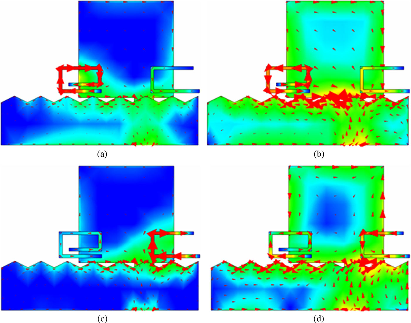
Fig. 2. Distribution of surface current at (a) 3.5 GHz (WiMAX notch band), (b) 4.28 GHz (pass band), (c) 5.45 GHz (WLAN notch band), and (d) 8.0 GHz (pass band).
The real and imaginary part of the input impedance of the presented antenna with and without resonators is displayed in Fig. 3. It can be noticed from the figure that the real and imaginary parts of the input impedance of the antenna without notch bands are, respectively, very much close to 50 and 0 Ω characteristic line and demonstrate a good impedance matching resulting in a ultra-wide operating band. On the other hand, at around 3.5 and 5.45 GHz, the real and imaginary parts of the input impedance of the antenna with notch bands are, respectively, much away from the 50 and 0 Ω characteristic impedance line and exhibit higher impedances resulting in a mismatching. Due to this mismatching, two notch bands are created at around 3.5 and 5.5 GHz that cover the WiMAX and WLAN bands, respectively.
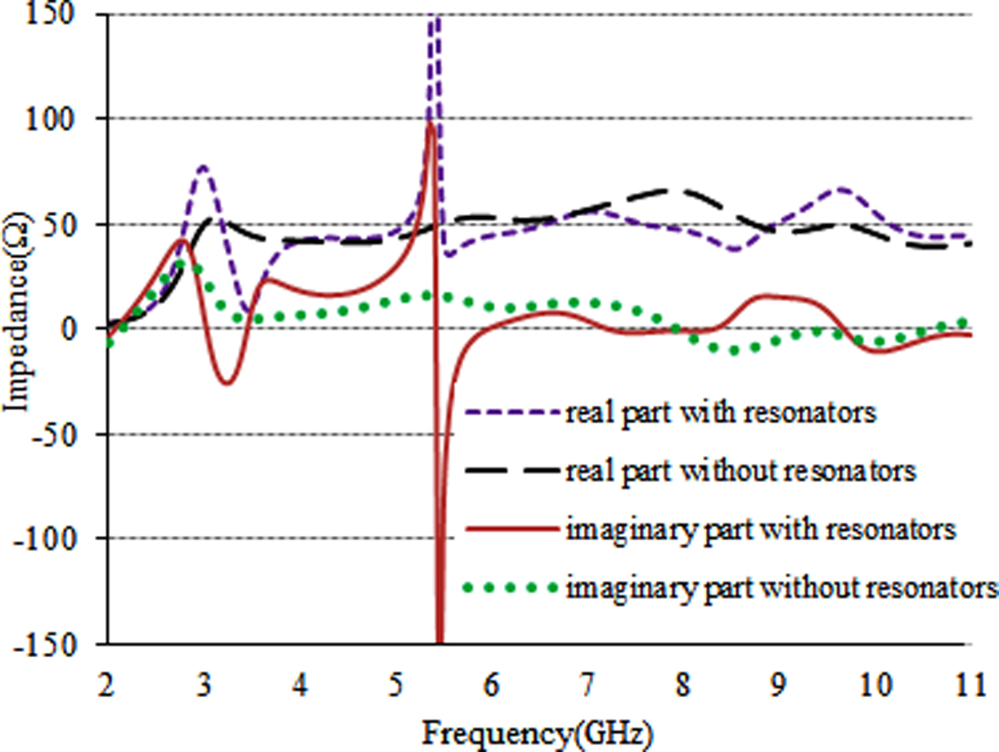
Fig. 3. Real and imaginary parts of the input impedance.
A parametric study is conducted to investigate the effects of different electrical and geometrical parameters on the performances of the presented antenna. As the parasitic resonators create the notch bands, their position and sizes have a great influence on band-notch characteristics and are studied. The entire sensitivity test is done by IE3D simulator from Zeland and during the simulations all but the parameter of interest are kept constant. The length of the first resonator L 1 has a significant role in the creation of notch bands. Figure 4(a) presents the VSWR for different L 1. The effect of length L 1 is significant at WiMAX band where the current is concentrated around the first resonating element while it has a very little effect on WLAN band. The variation in L 1 at certain values causes reduction in BW of WiMAX notch band as well as shifting of center frequency from the desired one. In Fig. 4(a), the first resonator length of 25 mm has achieved the required notch band from 3.25 to 3.75 GHz with a VSWR ≥2. Figure 4(b) depicts the effect of the first resonator's inner side length b on band-notch characteristics. In this figure, it is seen that the side length b plays a vital role in notching WiMAX band while it does not affect the higher WLAN band. Figure 4(c) displayed the simulated VSWR with different L 2, length of the second resonator. Increasing and decreasing of L 2 from a certain value shifted the WLAN notch band, whereas this variation has no effect on lower WiMAX notch band. It can be noted from the plot that a length L 2 = 18 mm can notch a BW of 5.0–5.6 GHz to cover the WLAN band. The variation of VSWR with second resonator's inner side length g is demonstrated in Fig. 4(d). It can be observed that at lower notch band, this parameter has no effect, whereas at higher notch band, there is a strong dependency of center frequency of the WLAN notch band on g. Insertion of second resonator with an inner side length of 4 mm can successfully notch the desired WLAN band. The effects of all the parameters of resonates and their optimized values are summarized in Table 1 from where it can be commented that the BW and center frequency (f c) of WiMAX notch band are totally controlled by first resonator, whereas second resonator can solely generate and adjust WLAN notch band, i.e. each notch band is not affected by the generation of others.
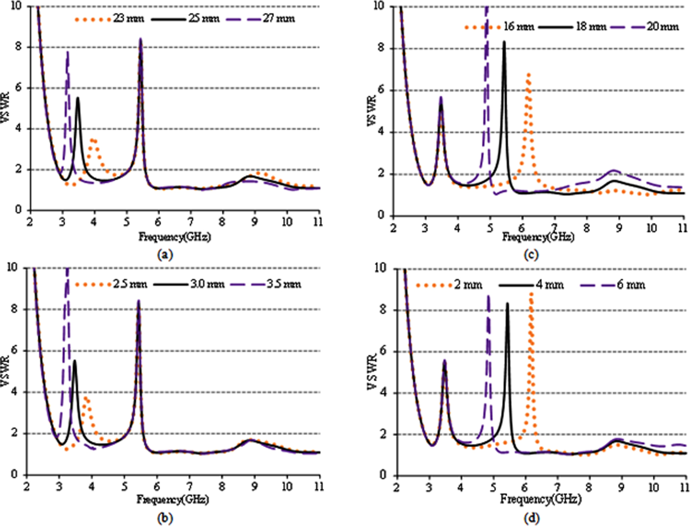
Fig. 4. Simulated VSWR for different values of (a) L 1, (b) b, (c) L 2, and (d) g.
Table 1. Effects of different parameters on first notch band (WiMAX) and second notch band (WLAN)

“▲” indicates increment from the optimized value, “▼” indicates decrement from the optimized value, “▬” means unaffected, and “×” indicates not done.
Results and discussion
The presented microstrip planar antenna has been simulated and optimized with method of moment-based simulator and then fabricated on FR4 printed circuit board for practical measurement. The measurement has been performed using N5227A PNA network analyzer (range 10 MHz–67 GHz) and SATIMO near-field antenna measurement system. Figure 5 displays the simulated and measured VSWR of the presented antenna in terms of frequency. In the simulation, the proposed antenna achieved impedance BWs ranging from 2.85 to 12 GHz to maintain a VSWR ≤2 with two notch bands of 3.26–3.72 and 5.09–5.60 GHz, whereas the BW in the measurement is from 2.98 to 12 GHz with the exhibitions of notch bands from 3.26 to 3.82 and 5.01 to 5.75 GHz. The displayed results are uniform over the whole operating band, although minimal inconsistencies are observed between the simulated and measured VSWRs. The discrepancy between simulated and measured results occurs given the feeding cable and fabrication inaccuracy.
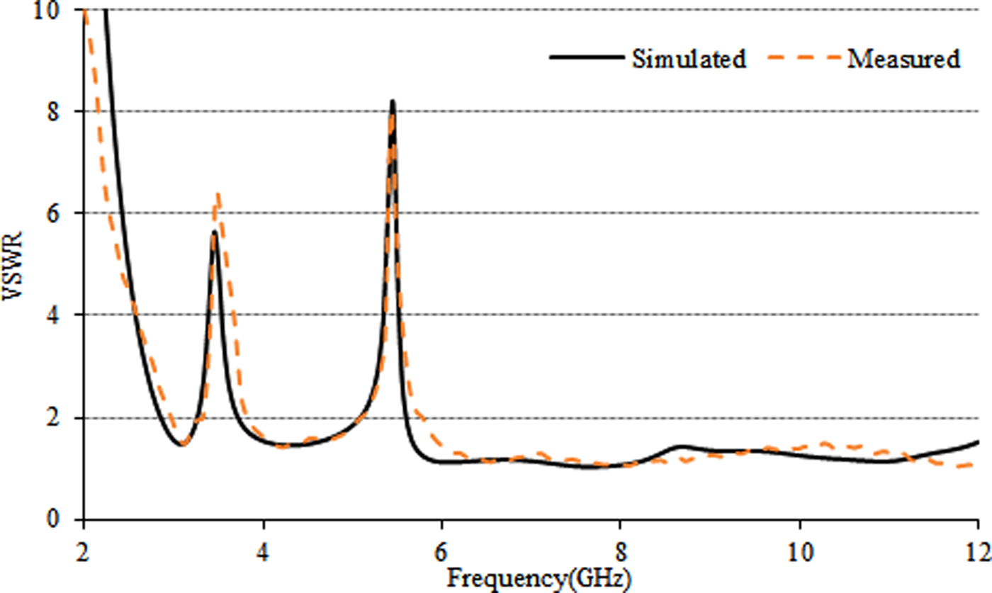
Fig. 5. Simulated and measured VSWR of the presented antenna.
The measured and simulated gains of the proposed antenna are reflected in Fig. 6. Despite of some disagreement especially at higher frequencies, the measured result significantly coincide with the simulated one. In this figure, the antenna has 7.05 dBi maximum gains with an average of 3.95 dBi. Sharp decrements of the gain have been observed at WiMAX and WLAN notch bands which indicate the effects of resonating elements.
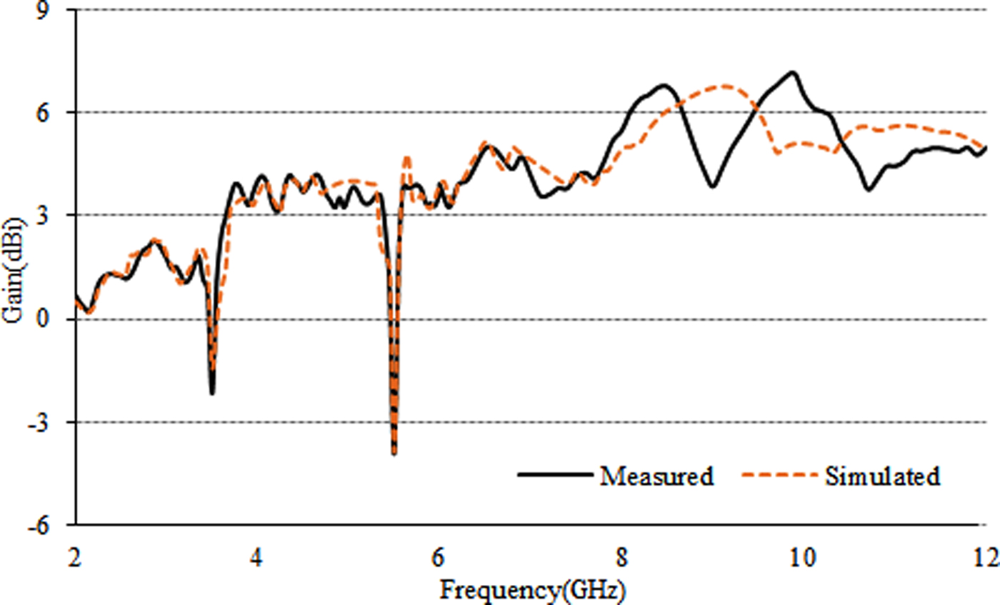
Fig. 6. Measured and simulated gain of the proposed antenna.
The radiation pattern of the presented antenna is measured in SATIMO StarLab system. The SATIMO StarLab system measures the antenna radiation patterns in near-field region using network analyzer and is shown in Fig. 7. Here, the data become far field considering the strongest forces of electromagnetic induction in this field. The near filed can mathematically be expressed by
 $$0.62\sqrt {\displaystyle{{D^3} \over \lambda}} \langle R\langle \displaystyle{{2D^2} \over \lambda}, $$
with R and D, respectively, are the far-field area and the maximum linear dimension of the antenna under test.
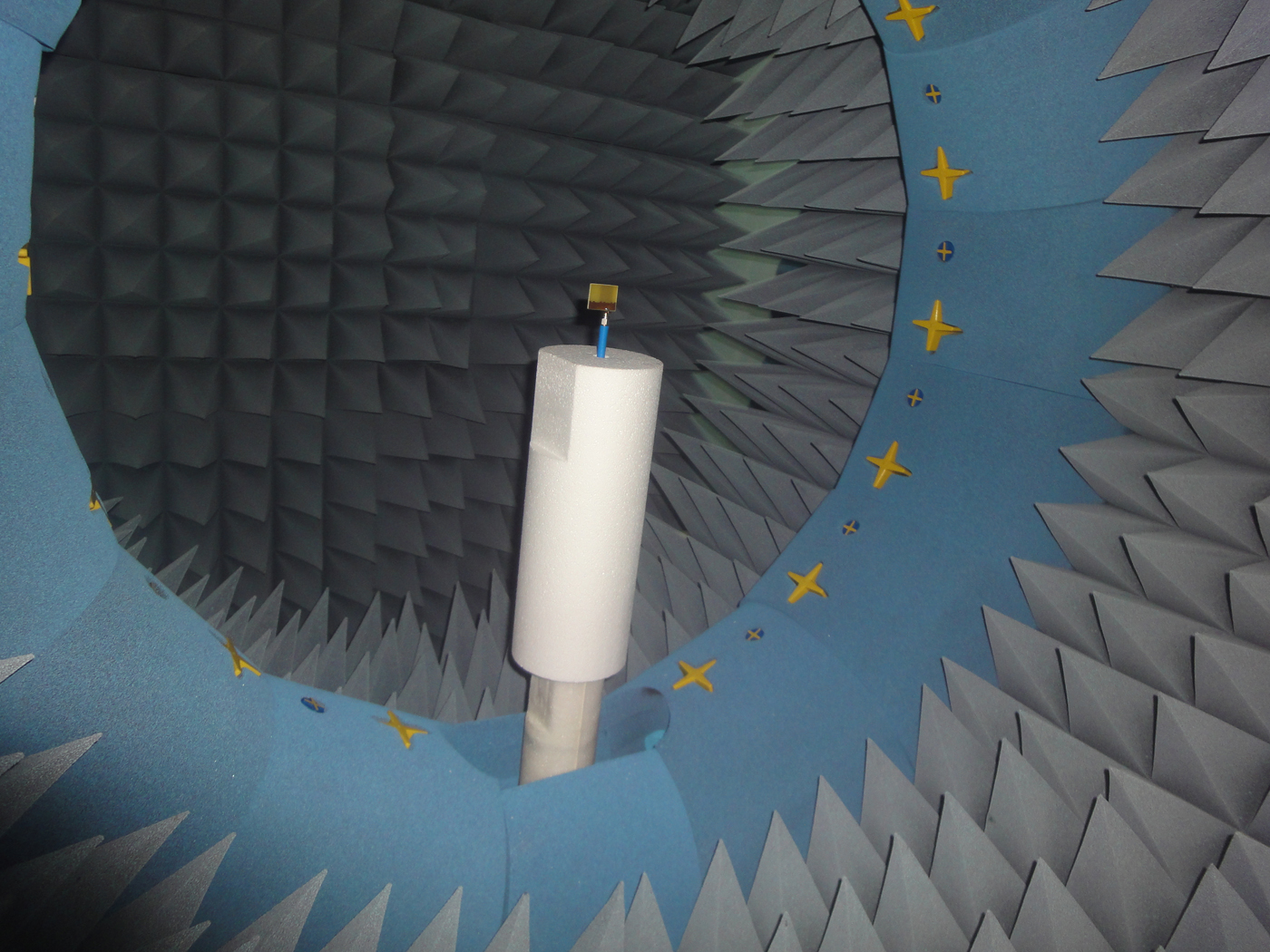
Fig. 7. Measurement set-up in SATIMO StarLab.
The far-field data are obtained from corresponding near-field data by using a Fourier transformation resulting in the generation of radiation pattern. The measured and simulated radiation patterns of the presented antenna with co-(Co-pol) and cross-polarization (X-pol) levels for same frequencies in E-plane (φ = 00) and H-plane (φ = 900) are plotted in Figs 8(a)–8(c). The radiation pattern at 3.0 GHz is omnidirectional in both E- and H-planes as shown in Fig. 8(a). The radiation pattern of the proposed antenna at 4.28 GHz remains appreciably durable to be omnidirectional. At a higher frequency of 8.0 GHz, the radiation pattern turns to be slightly directive due to higher-order current excitation. The cross-polarized level especially in H-plane increases with frequency which may be due to the radiation from the non-radiating edges of the proposed antenna. This high cross-polarized radiation may also be due to the unwanted higher order radiating modes that affect the far-field performance of the proposed antenna. Moreover, as the proposed antenna is designed on substrate with higher thicknesses and larger dielectric constant, this cross-polarized radiation becomes significantly prominent near the broadside direction in the H-plane which reflects the finding reported in [Reference Petosa, Ittipiboon and Gagnon14, Reference Bhartia, Bahl, Garg and Ittipiboon15]. This higher cross-polarized level can be suppressed by the use of modified feeding arrangement, exploration of defected patch surface, use of shorted patch, use of microwave absorbers, and metamaterials. Despite some nulls and higher cross-polarization level, the plot in Fig. 8 illustrates that the radiation patterns of the presented antenna are remarkably stable throughout the pass band of UWB spectrum.
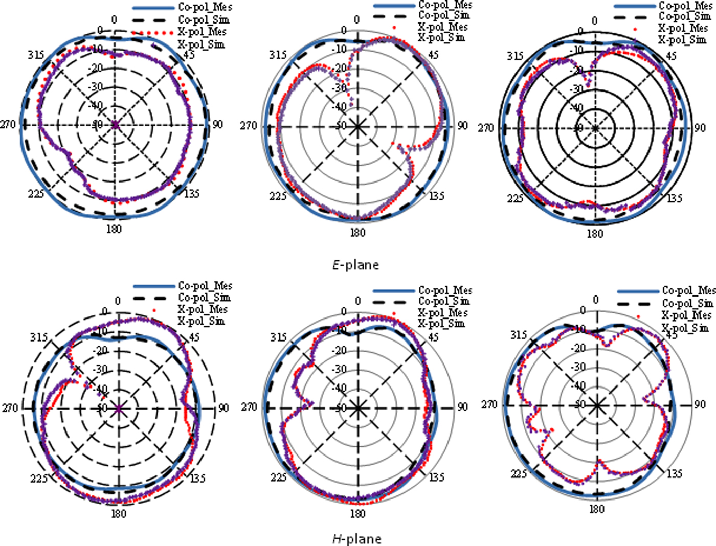
Fig. 8. Radiation patterns of the proposed antenna at (a) 3.0, (b) 4.28, and (d) 8.0 GHz.
Figure 9 depicts the measured group delay of the presented microstrip planar antenna. The group delay with minimum distortion is a prime requisite for time domain characteristic of the UWB antenna. The group delay that indicates the time delay of a signal can be expressed as the negative derivative of the phase to the frequency. To measure the group delay, two prototypes of the proposed antenna are connected to the two ports of the network analyzer. In this research, it is measured in face-to-face and side-by-side orientations and in both cases two antennas are separated by a distance of 250 mm. The measured group delays of the presented antenna are plotted in Fig. 8. The group delays during face-to-face and side-by-side positions, except for the notch bands, are linear and nearly same. This group delay corresponds well to the transmission characteristics of the antenna, thereby proving a minimal distortion of the transmitted signal.
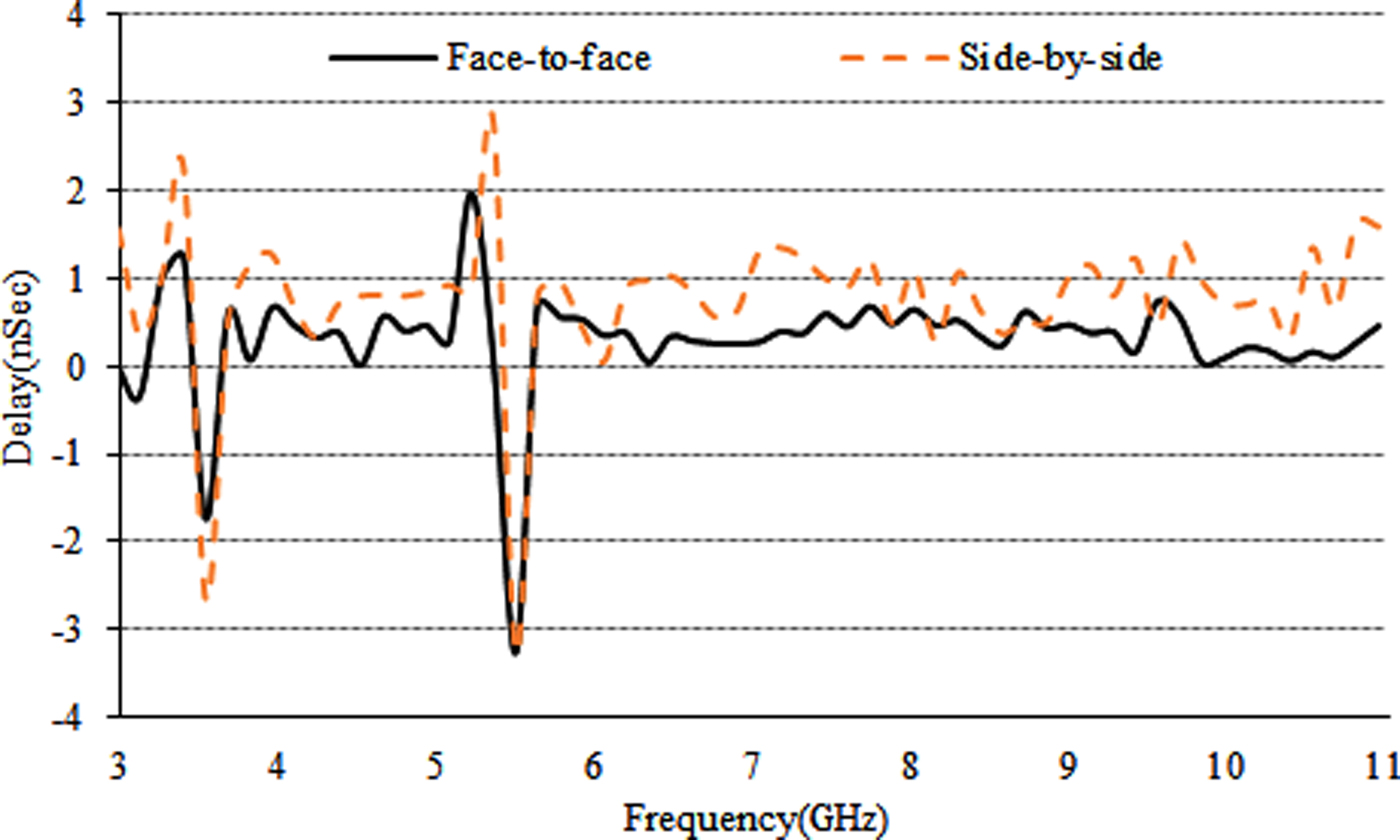
Fig. 9. Measured group delay of the proposed antenna.
In Table 2, the performance of the proposed antenna is compared with the recently reported other dual band-notch UWB antennas from where it is clear that there is a distinct trade-off between band-notch performance and size of the UWB antennas. From the comparison, it can be commented that the band-notch technique presented in this antenna has a distinct advantage over other designs as this technique possesses smaller footprint. Moreover, the proposed antenna has a small volumetric size, exhibits symmetric radiation patterns, and covers the entire UWB band with two notch bands.
Table 2. Comparison of the proposed antenna with recently reported dual band-notch UWB antennas

Conclusion
A compact low profile microstrip planar UWB antenna with dual-notched bands is presented. The antenna has a small size of 30 mm × 22 mm on a low-cost FR4 dielectric substrate. The dual-notched band is obtained by integrating two rectangular parasitic resonators beneath the radiating patch. Experimental result shows that the presented antenna could achieve a BW ranging from 2.98 to 12 GHz for VSWR ≤2 with two notch bands of 3.26–3.82 and 5.01–5.75 GHz. Both the simulated and measured results demonstrate that the proposed antenna has a good gain except at notch bands. The radiation patterns of the proposed antenna are also robust throughout the operating band and it also demonstrates linear time domain characteristics, hence is suitable for UWB wireless communication applications.
Author ORCIDs
Rezaul Azim, https://orcid.org/0000-0002-9648-7188
Acknowledgement
This work was supported by the University of Chittagong, Bangladesh under the grant number 5890/Ghobe/Pori/Praka/Doptor/CU/2017.
 A. K. M. Ariful Haque Siddique was born in Chittagong, Bangladesh. He received the B.Sc. and M.Sc. degrees in Electrical and Electronic Engineering from the University of Dhaka, Bangladesh. In 2014, he received the Ph.D. degree from the Department of Materials Science and Engineering in Chungnam National University, Daejeon, South Korea. In 2002, he has joined the University of Chittagong where currently he is working as an Associate Professor. He has been very promising as a researcher. He has authored and co-authored 10 referred journal articles, five international conference papers. His research interest includes the enabling technology for electronics, electronic communication system, and ultrasonic particle manipulation.
 Rezaul Azim was born in Chittagong, Bangladesh. He received the B.Sc. and M. Sc. degrees in Physics from the University of Chittagong, Chittagong, Bangladesh and the Ph.D. degree in Electrical, Electronic and Systems Engineering (Major in Telecommunication Engineering) from the Universiti Kebangsaan Malaysia (The National University of Malaysia). In 2005, he joined the University of Chittagong where currently he is a Professor. From August 2009 to September 2014, he was with the Department of Electrical, Electronic and Systems Engineering, Universiti Kebangsaan Malaysia as a Research Fellow. He has been very promising as a researcher with the achievement of several medals and awards for his research and innovation. He has filed 1 patent application. He has authored and co-authored 45 referred journal articles, 27 international and local conference articles, and two book chapters. His articles have been cited more than 972 times with an H-index of 16 (Source: SCOPUS). He is a reviewer of as many as 39 peer-review journals. He is a regular member of IEEE, IAENG, and Bangladesh Physical Society. His research interest includes the enabling technology for antennas and propagation, electromagnetics, microwave, and RF devices.
 Mohammad Tariqul Islam is a Professor at the Department of Electrical, Electronic and Systems Engineering of the Universiti Kebangsaan Malaysia (UKM) and visiting Professor of Kyushu Institute of Technology, Japan. He is the author and co-author of about 450 research journal articles, nearly 175 conference articles, and a few book chapters on various topics related to antennas, microwaves, and electromagnetic radiation analysis with 18 inventory patents filed. Thus far, his publications have been cited 4500 times and his H-index is 34 (Source: Scopus). His Google scholar citation is 6050 and H-index is 38. He is the recipient of more than 40 research grants from the Malaysian Ministry of Science, Technology and Innovation, Ministry of Education, UKM research grant, international research grants from Japan and Saudi Arabia. His research interests include communication antenna design, radio astronomy antennas, satellite antennas, and electromagnetic radiation analysis. Dr. Islam currently serves as the Guest Editor, SENSORS Journal, Associate Editor for IEEE Access and IET Electronics Letter. He received several International Gold Medal awards, a Best Invention in Telecommunication Award, a Special Award from Vietnam for his research and innovation, and Best Researcher Awards in 2010 and 2011 at UKM. He is the recipient of 2018 IEEE AP/MTT/EMC Excellent Award. He also won the best innovation award in 2011 and the Best Research Group in ICT niche in 2014 by UKM. He was the recipient of Publication Award from Malaysian Space Agency in 2014, 2013, 2010, 2009 and the Best Paper Presentation Award in 2012 International Symposium on Antennas and Propagation (ISAP 2012) at Nagoya, Japan and in 2015 in IconSpace. He is a Senior Member of IEEE, Chartered Professional Engineer-CEng, Member of IET (UK), and member of IEICE (Japan).


