


Introduction
Three-dimensional printing (3D) and additive manufacturing (AM) of metallic materials are witnessing significant advances. Maturation of both research-grade and commercial production 3D printing equipment during the past two decades, along with an increased diversity of feedstock materials, has spurred significant research activities across academic, government, and industrial research institutions worldwide. The most prominent forms of 3D metal printing involve powder beds, streams of gas-propelled powder jets, or wire for feedstock, lasers and electron beams as the energy sources, and precision automation equipment for digitally directing the energy source, the feedstock, or both along the material/energy deposition pathways required to form the desired shapes, layer by layer.
The potential for fabricating metal components directly from digital data using a single piece of fully automated equipment and feedstock materials and without additional hard tooling is very significant. Immediate near-term impacts include dramatic reductions in cost and lead time, the ability to produce small-lot or “one-of-a-kind” components on demand, and the ability to prototype and produce advanced, high-performance, and more efficient components that cannot be manufactured through conventional methods due to inherent limitations on geometry, material, microstructure, and properties. These benefits have been recognized and metal 3D printing is in use today for limited production by industry, R&D institutions, and governments across the globe.
While the advantages of 3D metal printing are compelling, there are also significant scientific and technical challenges that confront widespread implementation and adoption of these technologies. First, the microstructures and crystal textures produced through layerwise additive consolidation are quite novel, and rarely resemble those produced through conventional manufacturing methods such as casting or deformation processing. Second, the physical processes associated with incremental consolidation of metals accompanied by diverse variations in feedstock materials, processing parameters, processing protocols, and equipment architectures are inherently complex, leading to a diversity of “as produced” microstructures and properties. Third, comprehensive understanding of structural and microstructural defects present in metals processed through 3D printing/AM techniques and post-processing protocols such as heat treatment and hot-isostatic pressing cycles to alleviate these defects, as well as to transform the microstructures to those acceptable for service conditions, is limited and is a focus of intense investigation across R&D organizations.
The articles in this issue of MRS Bulletin focus on recent advances in 3D printing of metallic materials. They highlight scientific and technical challenges that need sustained and focused collaborative efforts in order to mature and transition 3D printing of metals for widespread adoption across diverse industries.
Brief history of metal 3D printing
Modern 3D printing is a recent development, considering that manufacturing dates back to antiquity. While the “age of modern 3D printing” can be considered to have started in 1987, with the first commercially produced 3D printer (SLA-1, 3D Systems), the approach of constructing metal parts using additive approaches dates back over 100 years. Reference Bourell1 The earliest known “cut and stack” approaches to layered part construction was by J.E. Blanther, who patented a process for cutting and stacking sheets of wax plates to create a die set for pressing paper sheets. Reference Blanther2 DiMatteo and Nakagawa Reference DiMatteo3–Reference Nakagawa, Kunieda and Liu5 later applied this layered approach to metal plates. The process involved cutting sheets of metal using a milling cutter, stacking the pieces to create the object, and then finishing the part to remove the roughness associated with stair-step edges ( Figure 1 ). Another early approach to 3D printing of metals was based on weld overlay, which involves laying down weld beads atop one another to construct a 3D shape. The earliest known example comes from Baker in 1925 ( Figure 2 ). Reference Baker6

Figure 1. Cut-and-stack approach for production of layered parts. Reference Blanther2

Figure 2. Weld overlay approach to 3D printing. Reference Baker6
The first use of a modern 3D printer to create a metal part was laser sintering of a copper-solder mixture by Bourell in 1990. Reference Manriquez-Frayre and Bourell7 The object formed from 72 layers is shown in Figure 3 . Indirect approaches to laser sintering of metals using transient polymer binders were commercialized in the mid-1990s. The University of Texas at Austin began work on a direct selective laser sintering (SLS) research system around 1991. Reference Das, McWllliams, Wu and Beaman8–11 Second-generation and third-generation research systems were developed in the mid- to late-1990s. Reference Moore12,Reference Das13 Das and Beaman patented direct SLS of metals in 2004. Reference Das and Beaman14 Direct metal laser melting was developed in Belgium and Germany. Kruth’s group at KU Leuven in Belgium worked with metal laser melting since 1991, and the company Layerwise, acquired by 3D Systems in 2014, was founded specifically to commercialize the formation of metal parts using powder bed processing. Meiners at the Fraunhofer Institute for Laser Technology in Germany was the first to use the term “selective laser melting” (SLM) in a German patent later filed in the United States. Reference Meiners, Wissenbach and Gasser15 High-energy fiber lasers were the principal energy source for this direct metal processing approach. A few years later, SLM Solutions, based on SLM technology, was formed in a split of companies from MCP-HEK in Germany.

Figure 3. The first direct metal part created using 3D printing. The part was approximately 7 cm in diameter. Reference Manriquez-Frayre and Bourell7
Powder bed metal 3D printing using an electron-beam energy source was developed in collaboration with Chalmers University of Technology in Gothenburg, and Arcam AB was founded in Sweden in 1997. The first production model, the EBM S12, was offered in 2002. Reference Wohlers and Gornet16
Keicher and co-workers at Sandia National Laboratories in the US invented the first directed energy deposition approach. Reference Jeantette, Keicher, Romero and Schanwald17 The technology, termed laser engineered net shaping (LENS), was commercialized by Optomec in the early 1990s with the first machine shipment in 1998.
Ex One was founded as Extrude Hone and had its first machine installed, the ProMetal RTS-300, in 1998. The process uses a binder to process metal parts in a powder bed, followed by binder burnout and densification.
Ultrasonic consolidation was commercialized by Solidica in the United States. Technical details of the process were released in 2001, and the first beta machines were shipped in late 2001 and early 2002. Reference Wohlers and Gornet16
Metal 3D printing methods
Various metal 3D printing methods utilizing a variety of energy sources and feedstock materials are in use today. For the purposes of this article, only direct metal fabrication methods are considered and indirect methods involving the printing of a shape followed by subsequent thermal treatment for sintering or infiltration are not covered. Direct metal printing methods can generally be categorized as laser-based, electron-beam-based, arc-based, and ultrasonic welding-based. Each of these categories are discussed.
Laser-based metal 3D printing methods
Laser-based metal 3D printing methods are classified into laser sintering (LS), laser melting (LM), and laser metal deposition (LMD). Reference Basak and Das18 LS is a powder bed fusion 19 technique in which a scanning laser is used to consolidate sequentially deposited layers of a metal powder. Different types of lasers including CO2, disk, Nd:YAG, and fiber lasers are used. The principal consolidation mechanism is liquid-phase sintering involving partial melting and coalescence of the powder. Pure, multicomponent, and pre-alloyed powders have been processed through LS.
Laser melting is a second powder bed fusion technique involving the consolidation of metal powders using powerful lasers. While the equipment setup and configuration and processing methodology are similar in LS and LM, in LM, the powder is completely or nearly completely melted to produce a fully dense or nearly fully dense structure. LM thus produces metal articles with a higher level of microstructural homogeneity compared with LS. LM is the predominant method for powder bed fusion-based metal 3D printing and is used to process pure metal powders as well as a range of alloys.
Laser metal deposition (LMD) is a directed energy deposition (DED) technique. 19 In LMD, the feedstock material can be a powder or wire. In powder-based LMD, the powder is conveyed by a pressurized-gas-delivery system through a nozzle or multiple nozzles into a melt pool created by a laser beam on a substrate. The laser and powder delivery system are moved along programmed paths to produce deposits of the desired thickness on the substrate. The LMD process can be used to repair and build monolithic objects as well as to produce functionally graded structures. In wire-feed LMD, instead of a powder, a wire is continuously fed into the path of the laser. The tip of the wire is continuously melted to create deposits on a substrate and nearly 100% of the wire is consumed, resulting in a higher material utilization efficiency than with powder. The combination of readily available lower-cost feedstock material in wire form, combined with high deposition rates, makes the wire-feed LMD process highly cost competitive for the rapid fabrication of net-shape components.
Electron-beam melting-based metal 3D printing methods
Electron-beam melting (EBM)-based metal 3D printing methods involve either a powder bed or wire feed to supply the feedstock material. 19 In the powder bed version, an electron beam is scanned across the powder bed in multiple passes at low power to preheat the powder to around 80% of the melting point. The beam is then scanned at high power to melt the powder. Processing takes place under a vacuum of 10–2 Torr with helium gas bled near the build area to cool the component. Pure metal or pre-alloyed powders are used and are completely melted during processing to produce fully dense or near-fully dense products. In the wire-feed version of EBM, a wire is continuously fed into the melt pool under a focused electron beam in a high-vacuum chamber (10–2 Torr or less). Material utilization is nearly 100% and power efficiency is nearly 95%, making the process highly competitive. Reference Taminger and Hafley20 Multiple wires can be used to produce functionally graded parts or parts with custom alloy compositions.
Arc-based metal 3D printing methods
Arc-based metal 3D printing methods are examples of DED. In these processes, an electric arc is created between a base material and a consumable rod comprising the feedstock material. The rod is completely melted and fed into the melt pool to create a weld deposit. Several variations exist, including shielded metal arc welding (SMAW), gas metal arc welding (GMAW), shaped metal deposition (SMD), 3D microwelding (3DMW), and plasma arc welding (PAW). Reference Weman21
Ultrasonic welding-based metal 3D printing methods
Ultrasonic AM (UAM) Reference White22,Reference White23 is an innovative process that uses thin (150 mm) metallic tapes as feedstock to manufacture complex structures by combining ultrasonic seam welding and intermittent machining. The UAM process has been scaled to large sizes and also for difficult-to-join materials by deploying it in a large machining envelope and increasing the power of the ultrasonic horn, respectively. Reference Fujii, Sriraman and Babu24 Recently, Hahnlen and Dapino et al. demonstrated manufacturing of AM components with embedded sensors and smart materials using this method. Reference Hahnlen and Dapino25
Material systems
Various types of metallic materials have been processed through metal 3D printing. These include pure metals (gold, copper, niobium, tantalum, titanium), alloy powders (aluminum-based, cobalt-based, copper-based, iron-based, nickel-based, and titanium-based), and powder mixtures (copper-based, iron-based, and graded compositions such as Ni-Al, Ti-Ni, Ti-Mo, and Ti-V).
Pure metals processed through metal 3D printing include titanium processed through LS, Reference Fischer, Leber, Romano, Weber, Karapatis, Andre and Glardon26 LM, Reference Santos, Osakada, Shiomi, Kitamura and Abe27 and LMD, Reference Santos, Osakada, Shiomi, Kitamura and Abe27,Reference Xue, Krishna, Bandyopadhyay and Bose28 tantalum through LMD, Reference Balla, Bodhak, Bose and Bandyopadhyay29 gold through SLM, Reference Khan and Dickens30 copper through LM and EBM, Reference Pogson, Fox, Sutcliffe and O’Neill31,Reference Ramirez, Murr, Martinez, Hernandez, Martinez, Machado, Medina, Frigola and Wicker32 and iron and niobium through EBM. Reference Murr33 A large body of research exists on metal 3D printing with alloy powders. Alloy systems include Al-, Co-, Cu-, Fe-, Ni-, and Ti-based ones with most of the processing done using LM or LMD. The Ding et al. article in this issue discusses aluminum alloys, including Al-40Ti-10Si, Reference Singh, Roy, Mitra, Rao, Dayal, Raj and Manna34 Al-Si-10Mg, Reference Buchbinder, Schleifenbaum, Heidrich, Meiners and Bültmann35,Reference Brandl, Heckenberger, Holzinger and Buchbinder36 and Al-15Cu. Reference Pinto, Cheung, Ierardi and Garcia37 Cobalt-based alloys include Co-29Cr-6Mo processed through SLM, Reference Takaichi, Nakamoto, Joko, Nomura, Tsutsumi, Migita, Doi, Kurosu, Chiba, Wakabayashi, Igarashi and Hanawa38 Co-26Cr-6Mo-0.2C processed through EBM, Reference Gaytan, Murr, Martinez, Martinez, Machado, Ramirez, Medina, Collins and Wicker39 and a range of alloys processed through laser cladding (DED as applied to coat other structures). Reference Frenk and Kurz40–Reference Ram, Esplin and Stucker44 Copper-based alloys processed include a special Cu-based alloy Reference Tang, Loh, Wong, Fuh, Lu and Wang45 and Cu-30Ni processed through direct metal deposition. Reference Bhattacharya, Dinda, Dasgupta, Natu, Dutta and Mazumder46 Iron-based alloys that have been processed include stainless steels, tool steels, and alloy steels through LM, LMD, and EBM.
A wide range of nickel-based superalloys have been processed through various metal 3D printing methods (see the article by Attallah et al. in this issue). The alloys IN625 and IN718 have received a great deal of attention Reference Das, Wohlert, Beaman and Bourell47–Reference Jia and Gu51 with processing methods including direct selective laser sintering, SLM, LMD, and EBM. A range of so-called “non-weldable” nickel-based superalloys for application in the hot section of gas turbines have also been successfully processed through SLM, scanning laser epitaxy (SLE), LMD, EBM, and SMD techniques. For example, SLM was used to process Waspalloy, Reference Mumtaz, Erasenthiran and Hopkinson52 MAR-247, Reference Ramos, Murphy, Lappo, Wood, Bourell and Beaman53 and CM247LC, Reference Carter, Martin, Withers and Attallah54 while SLE was used to process IN100, Reference Acharya and Das55 René 80, Reference Acharya, Bansal, Gambone, Kaplan, Fuchs, Rudawski and Das56 MAR-M247, Reference Basak and Das57–Reference Basak and Das59 René 142, Reference Das, Acharya, Bansal and Gambone60 CMSX-4, Reference Acharya, Bansal, Gambone and Das61–Reference Basak, Acharya and Das63 and René N5. Reference Basak and Das64–Reference Basak, Acharya and Das67 Various LMD processes have been applied to hot-section alloys. DMD was used to create deposits of René N4 Reference Santos, Kida, Carroll and Vilar68 and René N5. Reference Liu and Qi69 LMD was used to fabricate components in René 41. Reference Li and Wang70 The LENS process was used to process alloy IC221W and ELMF, while a similar process was used to deposit single-crystal CMSX-4. Reference Gäumann, Henry, Cleton, Wagniere and Kurz71 A microlaser-aided LMD process was used to produce crack-free samples of alloy IN100. Reference Horii, Kirihara and Miyamoto72 Laser powder buildup welding was shown to produce deposits in alloy MAR-M002. Reference Krause73 The EBM process has been used to produce structures in René 142 Reference Murr74 and CMSX-4. Reference Ramsperger, Mújica Roncery, Lopez-Galilea, Singer, Theisen and Körner75
Titanium alloys have been processed by various techniques—work has predominantly been done on Ti-6Al-4V (see the article by Qian et al. in this issue). In the late 1990s, in one of the first demonstrations of direct metal 3D printing of an actual component, direct SLS was used to fabricate a guidance section housing base for a US AIM-9 Sidewinder missile. Reference Amato, Gaytan, Murr, Martinez and Shindo49 More recent works include LM, Reference Das, Wohlert, Beaman and Bourell76 LMD, Reference Thijs, Verhaeghe, Craeghs, Van Humbeeck and Kruth77–Reference Brandl, Schoberth and Leyens82 EBM, Reference Puebla, Murr, Gaytan, Martinez, Medina and Wicker83–Reference Gockel, Beuth and Taminger86 gas tungsten arc welding, Reference Baufeld, Van der Biest and Gault87–Reference Baufeld, Brandl and Van der Biest89 and plasma deposition. Reference Martina, Mehnen, Williams, Colegrove and Wang90 Additionally, alloys such as Ti-24Nb-4Zr-8Sn, Reference Zhang, Klemm, Eckert, Hao and Sercombe91 Ti-6Al-7Nb, Reference Chlebus, Kuznicka, Kurzynowski and Dybala92 and Ti-6.5Al-3.5Mo-1.5Zr-0.3Si Reference Ren, Tian, Liu, Liu and Wang93 and titanium aluminides Reference Murr, Gaytan, Ceylan, Martinez, Martinez, Hernandez, Machado, Ramirez, Medina, Collins and Wicker94 have been investigated.
Microstructure and properties
Physical processes that control microstructure evolution during metal AM processes can be understood using knowledge from fusion welding, solid-state welding, and powder metallurgy. Reference Babu, Love, Dehoff, Peter, Watkins and Pannala95–Reference Babu97 All AM processes that rely on melting (such as DED, EBM, and SLM) use a moving energy source on top of the metal substrate or powder bed, which in turn leads to repeated melting, solidification, and solid-state transformation, as each and every layer is deposited. Interestingly, this condition is similar to multipass welding. Reference Reed and Bhadeshia98 Microstructure control during ultrasonic AM is defined by high strain rate thermomechanical deformation across the abutting interfaces, which is similar to solid-state welding. Reference Schick, Hahnlen, Dehoff, Collins, Babu, Dapino and Lippold99,Reference Shimizu, Fujii, Sato, Kokawa, Sriraman and Babu100 Furthermore, physical processes during binder jet process flow are similar to those in metal injection molding that is part of powder metallurgy technology. Reference German and Bose101
There are similarities in microstructure evolution in fusion-based metal AM and welding. Many independent variables (e.g., power, speed, preheat, gas shielding) common to welding are also relevant for metal AM with additional degrees of freedom. For example, metal AM equipment often changes the spatial locations (i.e., x, y) of the energy source by changing the scan location at each and every layer, as a function of geometrical cross section dictated by the computer-aided design file. These complex boundary conditions lead to highly transient heat and mass transfer conditions and result in microstructural heterogeneities within the build volume. These heterogeneities span from the nano- to the macrolength scales and often require detailed characterization.
One example of such data from a nickel-based superalloy (IN718) build made by a DED process Reference Tian, McAllister, Colijn, Mills, Farson, Nordin and Babu102 is presented in Figure 4 . Reference Kelly103 Due to the spatial motion of the energy source with reference to the build direction (x-, y-, and z-directions), it is often necessary to characterize the build in different sections (i.e., longitudinal, transverse, and horizontal [see Figure 4b]). Optical microscopy of these sections shows the complex nature of the molten pool shape in each and every layer (see Figure 4c), similar to multipass welding. These variations lead to significant mechanical heterogeneity measured by hardness mapping (see Figure 4d). Subsequent characterization showed large variations in crystallographic texture influenced by spatial variation of the molten pool shape, thermal gradient (G), and liquid–solid interface velocity (R), which in turn switches the solidification mode from the formation of columnar to equiaxed grains (see Figure 4e). Interestingly, the crystallographic heterogeneity did not correlate with the mechanical heterogeneity.

Figure 4. (a) Schematic illustration of direct energy deposition process. Adapted with permission from Reference Reference Kelly103. © 2004 Virginia Polytechnic Institute and State University. This process was used to manufacture a clad on an IN718 alloy substrate, followed by detailed characterization performed on the different sections shown in (b). Adapted with permission from Reference Reference Pogson, Fox, Sutcliffe and O’Neill31. © 2003 Emerald Group Publishing Ltd. (c) Macrostructure showing the tell-tale signs of deposition strategy in different cross sections from sample shown in (b). (d) Hardness mapping was performed across all cross sections and shows significant mechanical heterogeneity. (e) In addition, crystallographic heterogeneity across the transverse section was measured using electron backscatter diffraction imaging. (f) Scanning electron micrograph showing micron-scale heterogeneity of alloying elements within the γ dendrites due to solidification segregation. (g–h) High-resolution transmission electron microscope image showing the presence of γ″ microstructure within the γ grain. The identification of γ″ precipitates was further confirmed by high-resolution energy-dispersive spectroscopy (i–j) showing the presence of (i) high niobium concentration and (j) diffuse aluminum concentrations. Adapted with permission from Reference Reference Pogson, Fox, Sutcliffe and O’Neill31. © 2003 Emerald Group Publishing Ltd.
Further detailed analyses were performed using scanning and transmission electron microscopy (SEM and TEM). SEM confirmed chemical inhomogeneities due to solidification segregation (see Figure 4f). TEM confirmed the presence of γ″ phase (see Figure 4g–j) with associated niobium enrichment. This is indeed unexpected because γ″ is often formed after extended aging at high temperature. Reference Miller, Babu and Burke104 The energy-dispersive spectroscopy map for Al shows weak correlation with the γ″ precipitates. This accelerated precipitation was correlated to predicted thermal gyrations within a temperature range of 600 to 1000 K. Reference Makiewicz105
Based on the previous discussions, the obvious question is: Can we control microstructure evolution in AM using computational modeling and innovative process controls? Raghavan et al. recently answered this question using an EBM AM process. Reference Raghavan, Babu, Dehoff, Pannala, Simunovic, Kirka, Turner and Carlson106 First, innovative process control within the equipment that allows the operator to change melting conditions from linear line to spot mode was implemented. Reference Dehoff, Sames, Kirka, Bilheux, Tremsin and Babu107 Then, the line and spot melt pool conditions that shift G (thermal gradient) and R (liquid interface velocities) to alternate between columnar or equiaxed transition regions were designed using a high-performance computational tool (see Figure 5a). With these processing conditions, a build with predominantly columnar (see Figure 5b) or equiaxed (see Figure 5c) microstructure was achieved on demand. Note: this was performed with limited experimental trial-and-error optimization.

Figure 5. On-demand control of solidification texture within electron-beam melting builds: (a) Solidification map that predicts the probability of stray grains (equiaxed) and columnar grains. The circle symbols indicate the conditions that can be achieved during melting solidification within an electron-beam melting process. With these processing conditions that lead to linear- and spot-shaped melt pools, (b) columnar and (c) equiaxed grain structures were achieved throughout the build, respectively.
The previous demonstration leads to the next question: Is it possible to use model-based process parameters to achieve optimized low-temperature microstructure? Makiewicz et al. Reference Makiewicz, Babu, Keller and Chaudhary108 addressed this question. It is well known that the Ti-6A1-4V builds made by the DED process often lead to poor fatigue properties in the z-direction. Reference Kobryn and Semiatin109 This phenomenon can be correlated to mechanical (see Figure 6a) and microstructural heterogeneities (see Figure 6b). In this example, the top region of the build predominantly contains a basketweave microstructure (see the keys for microstructures in Figure 6c), while the bottom regions contained a colony microstructure. This abrupt transition was rationalized based on thermal excursions in these regions that were predicted using a computational model.

Figure 6. (a) Hardness map shows the heterogeneity from top to bottom of the Ti6Al4V clad made by the directed energy deposition process. (b) This heterogeneity was correlated to an abrupt change from basketweave (BW) to colony microstructure. (c) Key micrographs for different microstructures expected from Ti6Al4V are shown. (d) The change in microstructure shown in (b) was correlated to change in thermal cycles. (e) Hardness map shows comparably less mechanical heterogeneity with new processing conditions designed by computational models. Reference Makiewicz, Babu, Keller and Chaudhary108
Most of the time, the top regions of the build remain at temperatures higher than the β-transus (the temperature above which a single body-centered-cubic β phase is formed), and the final microstructure evolves during cooling from this high temperature after completion of the build. In contrast, the bottom regions undergo cyclic thermal gyrations below the β-transus temperature (see Figure 6d). With this understanding, a new set of processing parameters was designed that allowed for all of the build regions to be above the β-transus temperature throughout the build process. This required close control of processing parameters as a function of build height, while avoiding superheating of molten metal. With such a process control, a homogeneous microstructure was obtained (see Figure 6e). Such a homogeneous microstructure led to improved fatigue properties. Reference Prabhu, Chaudhary, Zhang and Babu110
Although the examples show the promise of obtaining microstructural control in the processing stage, common metal-AM-based defects such as porosity and lack of fusion, as well as optimization of microstructure, may require additional postprocessing such as hot isostatic pressing (HIP). Reference Murr, Martinez, Gaytan, Ramirez, Machado, Shindo, Martinez, Medina, Wooten, Ciscel, Ackelid and Wicker111
Current challenges and qualification issues
Although many published studies have shown the potential for deployment of metal-based AM, there are many challenges that limit the adoption of this technology across industries, especially the need for qualification of process and components. The process qualification can be performed by detailed logging and analysis of parameters during AM (see Figure 7 ). For example, fast Fourier transform analyses of the data (see Figure 7c) measured during long build cycles can be used as unique signatures that define successful or nonoptimal builds. Additional steps can include in situ monitoring of each and every layer using optical and thermal imaging. Reference Dinwiddie, Dehoff, Lloyd, Lowe and Ulrich112 These in situ thermal and optical data are then spliced together with process parameter log files and provided as boundary conditions to computational process and materials modeling. Reference Buchbinder, Schleifenbaum, Heidrich, Meiners and Bültmann35 These models will be able to predict any tendency for defect formation as well as microstructural heterogeneity. Reference Chaudhary113 In the next step, some of the sacrificial samples that are produced together with the component are characterized nondestructively with ultrasonics, Reference Lim, Yu, Cho, Farson, Babu, McCracken and Flesner114 computer-aided tomography using x-ray or neutron tomography, Reference Brandl, Heckenberger, Holzinger and Buchbinder36 as well as residual stress distribution. Reference Kolbus, Payzant, Cornwell, Watkins, Babu, Dehoff and Duty115

Figure 7. (a) Typical processing parameter data logged by an electron-beam melting process and (b) higher magnification shows the detailed variations of (from top to bottom) current, rake position, backing pressure, chamber pressure, and electron gun column pressure. (c) Analysis of the data with good time resolution allows for identification of unique signatures that can be used as process qualification. Reference Dinwiddie, Dehoff, Lloyd, Lowe and Ulrich112
The next step in qualification is the data set that can be used for component qualification. Schwalbach and Groeber Reference Schwalbach and Groeber116 recently demonstrated this by performing multi-model data collection and integration. An example of such multi-model analysis is shown in Figure 8 . A cylindrical component was manufactured concurrently with other components. While building, the process parameters were logged and analyzed further. The sample was nondestructively characterized by computer-aided tomography, which showed a reduced number density of pores below 15 mm height. This was correlated to the abrupt change in layer time, which is caused by other geometries that are being manufactured below 15 mm.
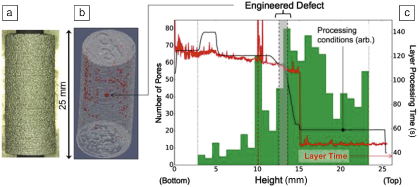
Figure 8. (a) Photograph of an example build that was used for component qualification. (b) Computer-aided tomography of the build that shows an engineered defect and porosity that formed due to processing (marked by red color). (c) Correlation of number of pores (green columns) to layer processing time (red line). Adapted with permission from Reference Reference Schwalbach and Groeber116. © 2015 AAAS.
Future trends
Applications of metal 3D printing are currently concentrated in the aerospace and biomedical sectors. Based on capital equipment and feedstock costs, current 3D printed parts are expensive compared to production parts, except when complex geometries are produced in short production runs. As metal 3D printing acceptance increases, it is anticipated that the manufacturing cost will decrease, which will open the application space to other sectors. Improvements to surface finish and part quality coupled to increase in the size of parts will open the application space to a wide variety of tooling applications. Research and development efforts today address the salient issues: machine cost (and build speed, which impacts the effect of machine cost on part cost), feedstock cost, surface finish, qualification and certification, and part size.
For the near term, machine cost is not anticipated to change materially. Fabricators of the most widely used 3D printing technologies incorporate high-powered lasers and electron beams that, with ancillary operating equipment, comprise a relatively high cost. With regards to build speed, a typical approach is to increase the energy-beam power and move at increased velocity. The result includes a change in cooling rate. For metals, the sensitivity of microstructure on cooling rate has a limiting effect on using this approach. Using multiple energy beams is a possibility, but this negatively impacts machine cost.
Feedstock cost is driven by market forces. In general, competition and production volume result in lower cost. For example, Alcoa recently announced that they are opening a 3D printing metal powder production facility outside Pittsburgh. The facility will produce titanium, nickel, and aluminum powders optimized for 3D printing.
Surface finish has been an ongoing challenge with 3D printing of metals from the beginning of the technology. One promising approach is to develop hybrid machines that perform usual sequential manufacturing steps in a more or less simultaneous fashion. Reference Lauwers, Klocke, Klink, Tekkaya, Neugebauer and Mcintosh117 For surface improvement in 3D printing, the secondary step is some form of subtractive manufacturing step. Matsuura in Japan was the earliest company to market a commercial laser melting machine with a milling cutter to finish surfaces during the part build. Geometric limitations are imposed that potentially limit the surfaces on a part that are possible to machine, and additional care must be taken with respect to part orientation as the build is prepared.
With regard to part size, Sciaky’s wire-fed electron-beam AM technology is an excellent example of large-scale printing, with part envelopes as large as 3.7 m × 1.5 m × 1.5 m. Critical surfaces must be finish machined. Other approaches are being considered, including the collaborative BAAM (big area additive manufacturing) technology developed by Oak Ridge National Laboratory and Cincinnati Inc. Presently, the process is used for plastics, principally acrylonitrile butadiene styrene, with a build chamber as large as 1.8 m × 3.6 m × 1 m and deposition rate as high as 100 lbs./h. Work is ongoing to develop the BAAM approach for metal processing. Further details of the BAAM process are discussed extensively in Reference Reference Jeantette, Keicher, Romero and Schanwald17. Alcoa has developed a combined 3D printing and forging technology termed Ampliforge. Reference Bush, Roegner, Colvin, Mueller, Rioja and Bodily118 Metallic parts are 3D printed and then forged. There are apparently geometric limitations on the parts, but the advantage is an improvement of mechanical properties compared to as-built parts without subsequent postprocessing.
In this Issue
Ding et al. provide an overview of the challenges and progress in terms of additive manufacturability of existing Al alloys. The article discusses the commonality of the physical processes, microstructure evolution, and property ranges achieved during casting, welding, and AM of non-heat-treatable and heat-treatable alloys. Based on the previous discussions, emerging technical pathways to address material deficiencies include infiltration methods.
Murr and Li focus on electron-beam melting and some of the unique microstructures that can be achieved using this process. For example, the feasibility of producing highly architectured microstructures with unique crystallography and phase balance during processing of nickel and titanium alloys. The authors also report the possibility of obtaining nonequilibrium microstructure in pure iron due to unique thermal signatures.
Dadbakhsh et al. review the mechanism of shape-memory NiTi alloy deformation, followed by coverage of laser-based AM approaches for direct manufacture of these alloys. The effect of processing on product microstructure and texture is considered. Mechanical properties are reviewed along with bioapplication issues of corrosion and biocompatibility. Potential biomedical applications of AM NiTi alloys are described.
Qian et al. highlight the most recent advances in laser- and electron-beam-based AM approaches for the popular structural titanium alloy Ti-6Al-4V in safety-critical applications. They show that the alloy can be processed such that the mechanical properties of as-built parts can compete successfully with mill-annealed parts when they are surface finished without heat treatment.
Attallah et al. provide an overview of the outstanding issues in AM of nickel-based superalloys from highly weldable to nonweldable alloys. They highlight the key challenges, including residual stresses and distortion, porosity and cracking defects, and anisotropy in microstructure and mechanical properties.
The Frazier sidebar article discusses the qualification of AM processes through integrated computational materials engineering (ICME). Advantages and challenges associated with this method are described. Finally, a three-tiered strategy adopted by the Naval Air Systems Command (NAVAIR) to accelerate the implementation of flight-critical metallic AM parts through ICME Informed Qualification is discussed.
An ICME informed approach to qualification for additive manufacturing
William E. Frazier (Naval Air Systems Command)
Additive manufacturing (AM) has been characterized as a potentially disruptive technology. It permits the rapid fabrication of components from 3D models. The disruptive aspects of the technology are numerous and will change the business calculus, the logistic supply chain, component design, and our engineering concepts of part realization. Unfortunately, the single biggest obstacle to widespread use of AM parts for structurally critical components are the cost and time associated with qualification and certification. This is where integrated computational materials engineering can help.
Qualification and certification
The terms qualification and certification are frequently used interchangeably or in unison in the context of technology. In this article, qualification refers to the manufacturing process used to produce a material and the means by which reproducible, reliable, minimum design material allowable properties are ensured. Certification refers to a specific part and whether it is fit for use in its intended operational environment.
A building-block approach has been used for decades for the qualification and certification of materials technologies and parts (see Figure 1 ). Reference Maher1 This is a tried and true means of ensuring safety and functionality, but is intrinsically linear in construct.
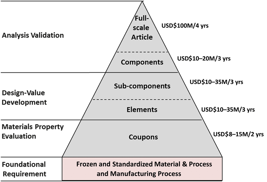
Figure 1. A building-block representation of the major challenges to qualification/certification of parts, showing the large cost and time associated with each phase of this process.
The qualification process requires that three basic questions be answered. Reference Frazier, Polakovics and Koegel2
-
1. Has the materials technology been developed and standardized? The process specification must be “frozen” (i.e., no modifications to key process parameters are permitted as these may affect material properties) and registered in accordance with an industry or military standard.
-
2. Has the materials technology been fully characterized? That is, have A-Basis mechanical property design allowables been developed? 3 These values, obtained through extensive testing of many material samples, indicate that at least 99% of the population of material values is expected to exceed the required tolerance with a 95% confidence level.
-
3. Has the materials technology been demonstrated? Representative subcomponent specimens must be fabricated and tested.
Certification of a part requires that it be tested in its intended operational environment and, depending upon the criticality of the component, tested at the system level. This process can cost millions of dollars and take over a decade to accomplish.
Unique characteristics and challenges of AM
AM provides the most value added when used for the production of geometrically complex, near-net-shaped products made from high-value alloys. The diversity of AM processes as well as the large number of key process parameters that change from build to build makes the use of traditional means of process qualification less than satisfactory. Reference Frazier4 The AM process is typically difficult to “freeze,” and microstructure, mechanical properties, and defect characteristics are very much dependent upon processing variables. Orientation, packing density, build path, energy density, raster rate, thermal profile, melt pool size, and substrate temperature are among the process variables that could impact part performance.
The very versatility and tailorability of the AM process that make it attractive for rapid, low-cost, low-production runs also means it can be too costly and time consuming to qualify small numbers of critical structural components. Consequently, there is a need to change the qualification paradigm away from statistically substantiated test data to a more integrated computational materials engineering (ICME) informed approach.
ICME informed qualification
ICME involves the application of high-fidelity, multiscale, computational modeling and simulation tools to the solution of materials engineering challenges. ICME should be broadly viewed as the integrated system of design, materials, manufacturing, and business modeling and simulation tools required for AM part realization linked together by a digital thread ( Figure 2 ). Reference Furrer and Schirra5–Reference Olson8

Figure 2. Components of integrated computational materials engineering (ICME) informed qualification and certification. Note: FEA, finite element analysis; FMEA, failure mode and effects analysis; AM, additive manufacturing.
ICME-informed AM process qualification is based upon the belief that ICME can be used to define a “quality” processing envelope for an AM process in n-dimensional variable space ( Figure 3 ). The ICME tools must account for all of the AM key process parameters and their interactions. Advanced sensors and controls are then needed in order to maintain the process within the quality envelope. Reference King, Anderson, Ferencz, Hodge, Kamath and Khairallah9
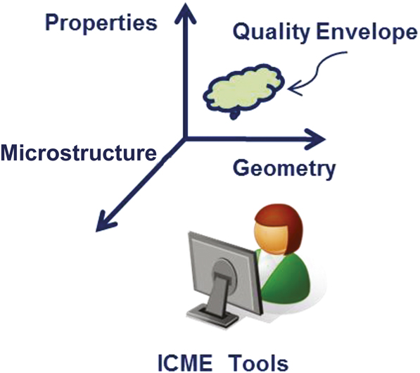
Figure 3. The n-dimensional variable space in integrated computational materials engineering (ICME) quality processing.
There are, however, real challenges associated with the implementation of ICME-informed AM process qualification. Among these challenges are the lack of physical property data, validated physics-based models for process and performance, process sensors, and control systems. Reference Cowles, Backman and Dutton10,Reference Reutzel11
The US Naval Air Systems Command, NAVAIR, has elected to tackle the problem of implementing flight-critical AM parts using an integrated, concurrent, three-tiered approach designed with the end state in mind (i.e., ICME informed qualification) (see Figure 4 ). AM part demonstrations are being used to develop the engineering confidence to fly aircraft with structurally critical metallic parts. This approach is referred to as a “point solution,” because it is applicable to a single part, made from a single material and single process using carefully controlled manufacturing. Point solutions tend to be expensive and are not readily extendable to the qualification/certification of other parts.
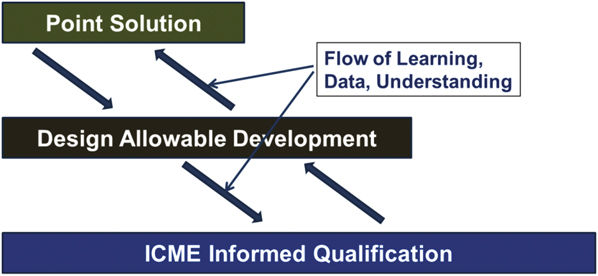
Figure 4. Strategic, three-tiered approach to additive manufacturing qualification. Note: ICME, integrated computational materials engineering.
In order to maximize the value of these point demonstrations, the execution of this strategy requires the systematic collection of the correct type of pedigreed material and process data (taken from materials whose complete processing history is known and documented), using state-of-the-art sensors and controls. The data collected then serve multiple functions and can be aggregated to generate useful specifications, standards, and design allowables, and can be used to help generate and validate the high-fidelity physics-based models required to implement ICME informed qualification.
The goal is to accelerate the widespread use of flight-critical AM parts. The belief is that ICME informed qualification can reduce the cost and time associated with this process.
Acknowledgments
Part of the research was sponsored by the US Department of Energy, Office of Energy Efficiency and Renewable Energy, Advanced Manufacturing Office, under Contract DE-AC05-00OR22725 with UT-Battelle, LLC. Research was also sponsored by the Laboratory Directed Research and Development Program of Oak Ridge National Laboratory, managed by UT-Battelle, LLC. The US Government retains and the publisher, by accepting the article for publication, acknowledges that the US Government retains a non-exclusive, paid-up, irrevocable, worldwide license to publish or reproduce the published form of this manuscript, or allow others to do so, for US Government purposes.


