Introduction
1951: The Beginning of Electron-Excited X-Ray Microanalysis
Electron-excited X-ray microanalysis (EPMA), in which a focused beam of energetic electrons excites characteristic X-rays from a volume with micrometer dimensions for elemental compositional measurement, was first demonstrated in a remarkable PhD thesis (University of Paris) by Castaing (Reference Castaing1951). In developing the prototype EPMA instrument, Castaing employed X-ray spectrometry based upon diffraction [“wavelength dispersive spectrometry” (WDS)], which was the only practical choice for X-ray spectrometry at that time. From his earliest WDS measurements, Castaing recognized that any quantification method that involved comparing one element to another would be impractical due to the complex behavior of the efficiency of the diffraction process as a function of photon energy. Moreover, the intensity measurements were further complicated since multiple diffractors were needed to cover the photon energy range of interest. To overcome this measurement challenge, Castaing proposed the standards-based intensity ratio (“k-ratio”) protocol. For each element in the unknown, the intensity, I X, for the same X-ray characteristic peak is measured in the unknown and in a standard, which can be a pure element or stoichiometric compound, under identical excitation conditions and at the same WDS diffraction setting, giving:
 $$k = \displaystyle{{I_{\rm X,{\rm unknown}}} \over {I_{\rm X,{\rm standard}}}}.$$
Since the WDS diffraction position and thus the WDS efficiency are constants for both measurements, the diffraction efficiency cancels quantitatively by taking the ratio of intensities. With this elegant solution to eliminate the need to accurately know the WDS efficiency, Castaing and others went on to establish the basis for performing quantitative elemental microanalysis through a series of multiplicative “matrix correction factors” applied to the k-ratio to yield the elemental concentration ratio (mass fractions) (Castaing, Reference Castaing1951; Heinrich, Reference Heinrich1981; Goldstein et al., Reference Goldstein, Newbury, Michael, Ritchie, Scott and Joy2018):
 $$k = \left[ {\displaystyle{{C_{{\rm unknown}}} \over {C_{{\rm standard}}}}} \right]ZAFc,$$
Z, the “atomic number correction” calculates the effects of electron energy loss and excitation loss due to electron backscattering
A, the “absorption correction” calculates the loss of characteristic photons due to photoelectric absorption while propagating through the specimen to escape in the direction of the X-ray detector
F, the “characteristic fluorescence correction” calculates the emission of characteristic photons from the subsequent de-excitation of the specimen atoms that were ionized in the photoelectric absorption process
c, the “continuum fluorescence correction” calculates the emission of characteristic photons following photoelectric absorption of the continuum (bremsstrahlung) X-rays that are also produced during energetic beam electron interactions with the specimen atoms.
All of the matrix correction factors depend on the composition of the unknown and the standard(s), so that starting with the normalized k-ratios as the initial estimate of the composition, the matrix correction factors must be iteratively calculated to reach a final result. Note that for this standards-based method, the raw analytical total, i.e., the sum of the concentrations of all constituents, will rarely be exactly unity because of the intensity and matrix correction uncertainties inherent in each elemental determination. Typically, the raw analytical total will range from 0.98 to 1.02. Deviations outside this range should be carefully examined. When measurement issues, such as dose, spectrometer performance, and instrumental drift, have been controlled, a low analytical total is a strong indicator of a missing constituent(s).
By the mid-1960s, the extensive efforts to understand and optimize the matrix correction factors had produced a mature measurement procedure. Testing of the analytical performance of this standards-based k-ratio protocol with matrix corrections was carried out with a suite of carefully developed standard reference materials, whose overall (bulk) composition was measured by independent methods and whose microscopic homogeneity was established by electron probe microanalysis studies (Goldstein et al., Reference Goldstein, Yakowitz, Newbury, Lifshin, Colby and Coleman1975). Taking these binary and multielement alloys and glasses as unknowns, analysis was performed with a standards suite consisting of pure elements and stoichiometric compounds for those elements incompatible with a vacuum or which suffered electron beam damage (e.g., CaF2, GaP, and FeS2 for S, which in pure element form deteriorates under electron beam bombardment). The figure of merit used to judge the EPMA result was the “relative error,” now described more correctly as the “relative deviation from the expected value (RDEV)”:
 $${\rm RDEV}\;\left( \% \right) = \left[ {\displaystyle{{\left( {{\rm measured}\;{\rm value} - {\rm true}\;{\rm value}} \right)} \over {{\rm true}\;{\rm value}}}} \right] \times 100\%. $$
The “true value” is the concentration of the element known from the independent analysis.
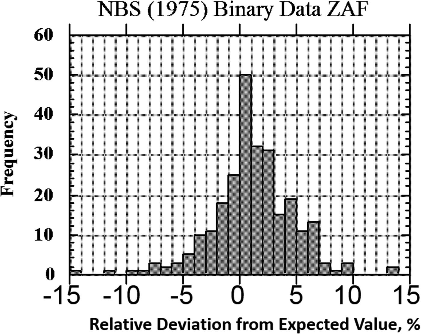
The result of one of these exercises to test EPMA-WDS for major constituents, arbitrarily defined as a mass concentration C > 0.1, is shown in the histogram of RDEVs presented in Figure 1. The suite of materials, binary and ternary metal alloys containing a wide range of elements, was analyzed with a beam energy of 20 keV and with characteristic X-ray peaks with energies above 1 keV, thus excluding a direct measurement of the low atomic number elements, e.g., F, O, N, C, and B. This RDEV histogram distribution can be described as having a standard deviation of 2.5% relative, so that 95% of the analyses fall within ±5% of the expected value.

Fig. 1. Histogram of RDEV for binary alloys and compounds; WDS spectrometry; major constituents; NBS ZAF corrections (Yakowitz, Reference Yakowitz, Goldstein, Yakowitz, Newbury, Lifshin, Colby and Coleman1975).
1968: Energy Dispersive X-ray Spectrometry Is Applied to EPMA
The enormous progress made in the 1960s in the development of solid-state (semiconductor) radiation detectors leads to the first implementation of an “energy dispersive X-ray spectrometer” [lithium-drifted silicon, “Si(Li)-energy dispersive X-ray spectrometry (EDS)”] on an EPMA in a watershed paper by Fitzgerald et al. (Reference Fitzgerald, Keil and Heinrich1968). This first-generation Si(Li)-EDS had very limited energy resolution, measured as the full peak width at half peak maximum intensity (FWHM), of approximately 600 eV over the photon energy range from 2 to 10 keV. This performance can be compared with the much better resolution of WDS, which produces 2–10 eV over this range depending on the diffractor. Despite the poor resolution, the value of EDS for qualitative analysis was immediately evident. By measuring the entire excited X-ray spectrum at every location sampled by the electron beam, EDS analysis greatly improved the efficiency of qualitative analysis of complex microstructures, where the composition could vary greatly from location to location. Qualitatively analyzing each measured location with WDS required scanning the wavelength range of two or more diffractors to cover the energy range of interest, a process that incurs a severe time penalty. Even with the earliest EDS detectors, the qualitative analysis could reveal the major constituents with every measurement, so that unexpected changes in composition could immediately be recognized.
The intense competition among the emerging EDS vendors leads to improvements in semiconductor detector manufacturing resulting in rapid advances in energy resolution. The resolution of Si(Li)-EDS, measured at the energy of Mn K-L2,3 (5.895 keV), reached a limiting value of approximately 129 eV FWHM with a maximum throughput [output count rate (OCR) versus input count rate (ICR)] of approximately 2,000 counts per second, where the ICR represents the photons that reach the entrance of the detector and the OCR represents the photons that are actually recorded. EDS vendors also exploited the extraordinary advances occurring in computing and mass storage hardware, developing control systems for EDS that included increasingly sophisticated software to aid in characteristic peak identification. Spectrum processing to extract the characteristic peak intensities from the continuum background enabled the demonstration of quantitative analysis that followed the Castaing k-ratio/matrix corrections protocol (e.g., Schamber, Reference Schamber1973; Ware & Reed, Reference Ware and Reed1973; Fiori et al., Reference Fiori, Myklebust, Heinrich and Yakowitz1976). The introduction of the silicon drift detector EDS (SDD-EDS) greatly advanced the performance of energy dispersive spectrometry (Streuder et al., Reference Streuder, Fiorini, Gatti, Hartmann, Holl, Krause, Lechner, Longoni, Lutz, Kemmer, Meidinger, Popp, Soltau and Van Zanthier1998 ). As subsequently developed, the SDD-EDS throughput increased by a factor as high as 75 (e.g., an OCR of 130,000 counts per second) for the same resolution compared with the earlier Si(Li)-EDS technology while simultaneously achieving extreme stability in terms of peak shape (resolution) and peak position (calibration) (Fiorini et al., Reference Fiorini, Frizzi and Longini2006). Because of the high throughput, spectra with 1 million counts or more (integrated between a threshold of 100 eV and incident beam energy, E 0) can be recorded in modest time (e.g., 10 s). The stability of the peak resolution and calibration is critical to the success of accurate fitting of the peak intensities, especially when two or more peaks interfere. This extraordinary performance of SDD-EDS has led to a new level of electron-excited elemental X-ray microanalysis (Newbury & Ritchie, Reference Newbury and Ritchie2015a).
At this 50th anniversary of the introduction of EDS to EPMA, what level of analytical performance can be achieved with energy dispersive spectrometry? This paper is not a comprehensive review of the extensive work of so many participants over nearly 70 years to create the technique of quantitative electron-excited EDS microanalysis. Rather, this paper seeks to demonstrate the accuracy of EDS analysis, as tested against materials of known composition, the precision of the EDS measurement of k-ratios compared with WDS, and the practical limit of detection that can be achieved. For this study, EDS spectra were collected on an extensive suite of micro-homogeneous materials of known composition using the vendor control software for the EDS system and file exportation with the Microscopy Society of America spectral format (.msa spectrum format, 1991). All quantitative calculations have been made using the open-access NIST EDS analytical software “NIST DTSA-II” (Ritchie, Reference Ritchie2018). It is reasonable to expect that similar analytical performance should be achievable with standards-based analysis implemented in vendor software.
Experimental Details
Materials
1. NIST microanalysis standards are certified both for bulk composition (listed in the results table for each SRM) and homogeneity on the micrometer lateral scale (NIST, 2018):
a. SRM 470 Mineral Glasses for Microanalysis
b. SRM 478 Microprobe Standard Cartridge Brass
c. SRM 479 Fe–Cr–Ni Alloy Microprobe Standard
d. SRM 480 Tungsten 20%–Molybdenum Alloy Electron Microprobe Standard
e. SRM 481 Gold–Silver Wires for Microprobe Analysis
f. SRM 482 Gold–Copper Wires for Microprobe Analysis
g. SRM 483 Fe–3Si Alloy Microprobe Standard
h. SRM 2061 TiAl(NbW) Alloy for Microanalysis
2. NIST SRM 610 Trace Elements in Glass, a bulk standard not certified for micro-homogeneity.
3. Stoichiometric compounds, e.g., borides, carbides, nitrides, oxides, sulfides, etc., obtained from various suppliers.
4. Prepared microprobe standards (Geller Microanalytical Laboratory, 426 Boston St, Topsfield, MA 01983, USA).
Sample and Standard Preparation
All bulk materials were prepared following conventional materialographic grinding and polishing procedures appropriate to each material to produce a highly polished surface. Insulating materials were coated by thermal evaporation with a carbon layer of 5–7 nm nominal thickness.
Analytical Details
A JEOL 8500F thermal field-emission gun electron microprobe equipped with a Bruker QUAD SDD-EDS was used for all measurements. A beam energy of 20 keV was selected for analysis of the SRMs, providing adequate overvoltage for the excitation of the high-photon energy K-shell and L-shell characteristic X-ray peaks. For the analysis of materials containing low atomic number elements, with characteristic X-ray peaks below 1 keV, the incident beam energy was reduced to 10 or 5 keV, depending on what other elements were present with the low atomic number element.
Certain commercial equipment, instruments, or materials are identified in this paper to foster understanding. Such identification does not imply recommendation or endorsement by the National Institute of Standards and Technology, nor does it imply that the materials or equipment identified are necessarily the best available for the purpose.
EDS Spectrum Processing
All spectra were collected with the vendor EDS operational software, exported through the .msa spectrum format (.msa spectrum format, 1991), and processed with the NIST DTSA-II EDS software (Ritchie, Reference Ritchie2018). DTSA-II employs a multiple linear least square peak fitting with measured (rather than theoretically modeled) peak references. Where possible, a pure element was used to provide the peak fitting reference(s) (i.e., measured characteristic X-ray peak or peak family) and to also serve as a compositional standard. For elements which are incompatible with the vacuum, e.g., oxygen, a stoichiometric compound, e.g., MgO, was used. Similarly, for pure elements that undergo electron beam damage, e.g., sulfur, a stable stoichiometric compound, e.g., FeS2, was used. The measured k-ratios are converted into concentration ratios (C unknown/C standard) by the application of matrix corrections (for electron retardation and backscattering, X-ray self-absorption, and secondary X-ray fluorescence following self-absorption of characteristic and continuum X-rays) based upon the Pouchou & Pichoir (Reference Pouchou, Pichoir, Heinrich and Newbury1991) formulation for the depth of the distribution of ionization.
The raw analytical total, which is the sum of all measured constituents, including oxygen, when calculated by the method of assumed stoichiometry, typically fell within the range 0.98–1.02 for analyses performed in the “conventional” beam energy range, 10–20 keV. The deviation of the analytical total from unity arises from the various sources of uncertainty in the measurement of the spectrum (e.g., differences in conductive coating thickness and oxide layers) and from uncertainty in the algorithms and parameters employed for the correction of matrix effects. The raw analytical total provides important information for the analyst. A raw analytical total below unity should be considered as a possible indicator of an unrecognized and unanalyzed constituent(s). Thus, when performing standards-based analysis, the raw analytical total should always be inspected by the analyst. Once the analyst is satisfied that all constituents are properly considered and the origin(s) for the deviation from unity is understood, it is reasonable to normalize the analytical total to unity to obtain the final concentrations. Normalization places the concentrations on a logical basis for comparison to other measurements or to ideal stoichiometric composition when the mass concentrations are converted to atomic concentrations.
After inspection of the raw total, normalization was applied to raw mass concentrations and RDEVs calculated with equation (3). For easier comparison to the formulae of stoichiometric compounds, atomic concentrations were calculated to determine the final RDEVs reported in the tables of results.
As part of the peak fitting procedure, NIST DTSA-II constructs the “peak fitting residual spectrum” which shows the intensity remaining in the channels over which the peak fitting has been performed for the designated suite of elements (Ritchie, Reference Ritchie2018). For situations where peak interference occurs, the peak fitting residual spectrum can reveal constituents whose peaks are hidden under the peaks of higher concentration constituents within limits imposed by the spectrum statistics (Newbury & Ritchie, Reference Newbury and Ritchie2018).
In the following discussion, these arbitrary terms will be used to broadly classify constituents:
“major”: mass concentration C > 0.1 mass fraction
“minor”: 0.01 ≤ C ≤ 0.1
“trace”: C < 0.01
Results
Analysis of Major and Minor Constituents in EDS Spectra with No Significant Overlaps
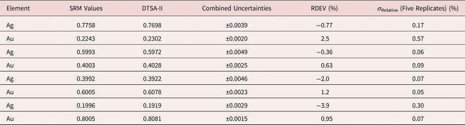
Tables 1–9 present quantitative results for NIST SRMs where all constituents fall within the major and minor constituent categories. For these particular SRM compositions, the EDS spectra have no significant interelement peak overlaps so that the main challenge to peak fitting is to separate the characteristic X-rays from the continuum X-ray background. The results in these tables include a total of 50 elemental determinations, and the distribution of RDEVs is such that 56% of the results fall within ±1% relative and 84% fall within ±2% relative. The largest RDEV value encountered was −3.9% for Ag in the 20Ag–80Au alloy.
Table 1. Analysis of NIST SRM 478 (Cartridge Brass) (E 0 = 20 keV; Pure Element Standards; K-Shell X-rays; Values in Normalized Mass Concentration; Combined Uncertainties Estimated from NIST DTSA-II).

Table 2. Analysis of NIST SRM 479 (Stainless Steel) (E 0 = 20 keV; Pure Element Standards; K-Shell X-rays; Values in Normalized Mass Concentration; Combined Uncertainties Estimated from NIST DTSA-II).
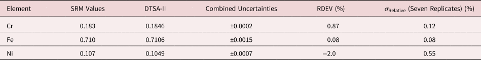
Table 3. Analysis of NIST SRM 480 (Molybdenum–Tungsten Alloys) (E 0 = 20 keV; Pure Element Standards; L-Shell X-rays; Values in Normalized Mass Concentration; Combined Uncertainties Estimated from NIST DTSA-II).

Table 4. Analysis of NIST SRM 481 (Gold–Silver Alloys) (E 0 = 20 keV; Pure Element Standards; Ag L and Au M; Values in Normalized Mass Concentration; Combined Uncertainties Estimated from NIST DTSA-II).

Table 5. Analysis of NIST SRM 482 (Gold–Copper Alloys) (E 0 = 20 keV; Pure Element Standards; Ag L and Cu K; Values in Normalized Mass Concentration; Combined Uncertainties Estimated from NIST DTSA-II).
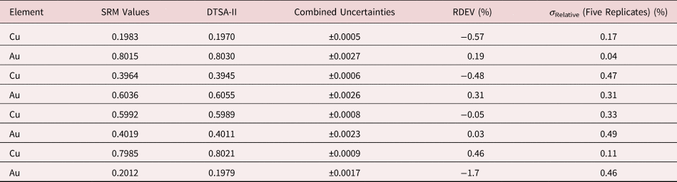
Table 6. Analysis of NIST SRM 483 (Fe–3Si Transformer Steel Alloy) (E 0 = 20 keV; Pure Element Standards; K-Shell X-rays; Values in Normalized Mass Concentration; Combined Uncertainties Estimated from NIST DTSA-II).

Table 7. Analysis of NIST SRM 2062 (Al–Ti–Nb–W Alloy) (E 0 = 20 keV; Pure Element Standards; Al K, Ti K, Nb L, W L; Values in Normalized Mass Concentration; Combined Uncertainties Estimated from NIST DTSA-II).
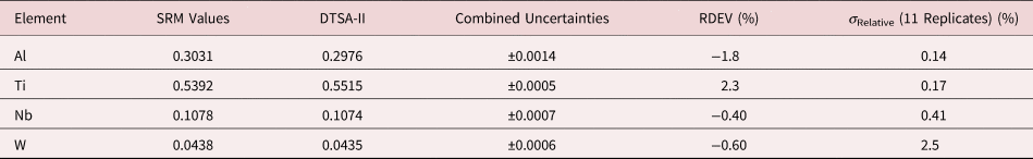
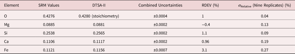
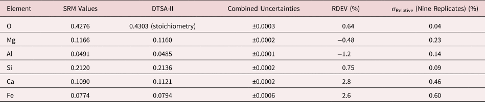
Table 8a. Analysis of SRM 470 (K411 Glass) (E 0 = 10 keV; Oxide Standards Except for Fe; O by Assumed Stoichiometry; K-Shell X-rays; Values in Mass Concentration; Combined Uncertainties Estimated from NIST DTSA-II.

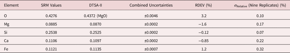
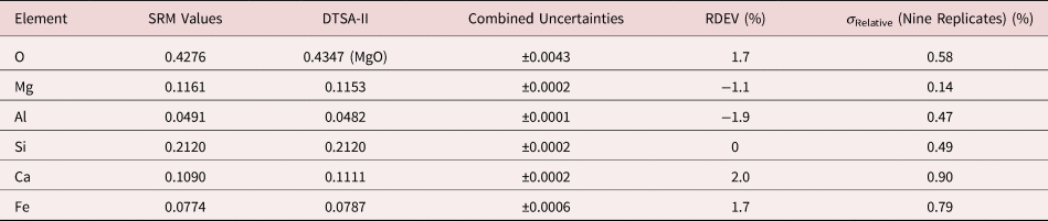
Table 8b. Analysis of SRM 470 (K411 Glass) [E 0 = 10 keV; Oxide Standards Except for Fe; O Directly Analyzed (MgO); K-Shell; Values in Mass Concentration; Values in Mass Concentration; Combined Uncertainties Estimated from NIST DTSA-II].

Table 9a. Analysis of SRM 470 (K412 Glass) (E 0 = 10 keV; Oxide Standards Except for Fe; O by Assumed Stoichiometry; K-Shell; Values in Normalized Mass Concentration; Combined Uncertainties Estimated from NIST DTSA-II).

Table 9b. Analysis of SRM 470 (K412 Glass) [E 0 = 10 keV; Oxide Standards Except for Fe; O by Assumed Stoichiometry or Directly Analyzed (MgO); K-Shell; Values in Normalized Mass Concentration; Combined Uncertainties Estimated from NIST DTSA-II].

Note that Tables 8 and 9 present results for the analysis of SRM Microanalysis Glasses by two methods: (1) direct analysis of oxygen with a standard (MgO) and (2) indirect analysis of oxygen based upon the method of the assumed stoichiometry of the cations. For both glasses, direct analysis of oxygen leads to larger values of RDEV, but the values obtained, 3.2% for O in K411 and 1.7% for O in K412, are still well within ±5% relative.
Analysis of Major Constituents with Significant Overlaps
None of the analyses reported in Tables 1–9 involves a significant peak overlap, so the main challenge to determining accurate peak intensities is the separation of the characteristic X-rays from the continuum X-ray background. The following examples involve severe peak overlap, where the separation of the peaks arising from different elements is substantially less than the nominal resolution of the EDS at that energy.
When considering these examples, the energy resolution of the EDS is needed at the appropriate photon energy of the interfering peaks. The energy resolution of the EDS, taken as the FWHM, is a function of the photon energy, E ν, and can be estimated with the following equation (Fiori & Newbury, Reference Fiori and Newbury1978):
 $${\rm FWHM}\left( {E_\nu } \right) = \left[ {2.5\left( {E_\nu - E_{{\rm ref}}} \right] + {\rm FWHM}_{{\rm ref}}^2 } \right]^{0.5}.$$
The subscript “ref” refers to the reference FWHM and photon energy at which the EDS performance is specified, and all terms in equation (4) are expressed in eV. Thus, for an EDS that produces an FWHM of 129 eV at the energy of Mn K-L2,3 (5,895 eV), equation (4) becomes:
 $${\rm FWHM}\left( {E_\nu } \right) = \left[ {2.5\left( {E_\nu - 5,895} \right] + {129}^2} \right]^{0.5}.$$
1. PbS
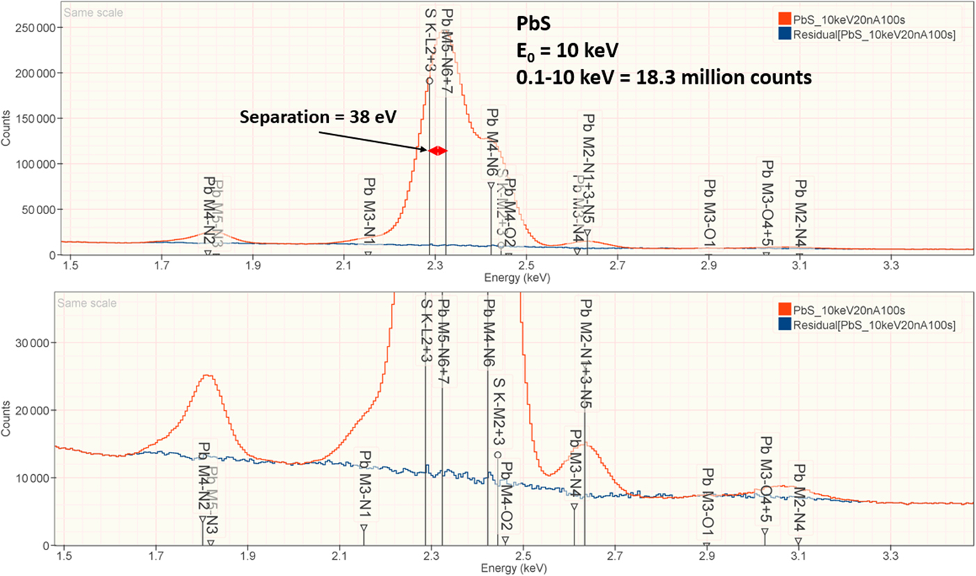
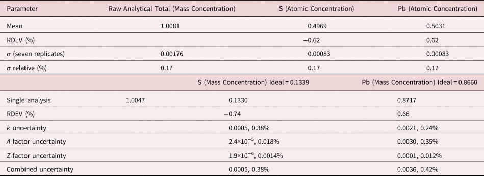
The analysis of PbS involves the interference of the S K-L2,3 at 2.307 keV and Pb M5-N6,7 at 2.345 keV, a separation of 38 eV at photon energy where the EDS resolution calculated with equation (6) is 88 eV, as shown in Figure 2. The NIST DTSA-II analysis of PbS at E 0 = 10 keV is given in Table 10 with concentrations expressed in atom fraction. RDEVs below 1% relative are obtained in this analysis.

Fig. 2. EDS spectrum of PbS (E 0 = 10 keV) showing the region of the S K-family and the Pb M-family; lower, the peak fitting residual spectrum (blue) after fitting for S and Pb.
Table 10. Analysis of PbS [E 0 = 10 keV; FeS2 and PbSe Used as Fitting References (S K-L2,3 and Pb M5-N6,7); CdS and PbSe as Standards; Values in Atom Concentration; Combined Uncertainties as Estimated from NIST DTSA-II].
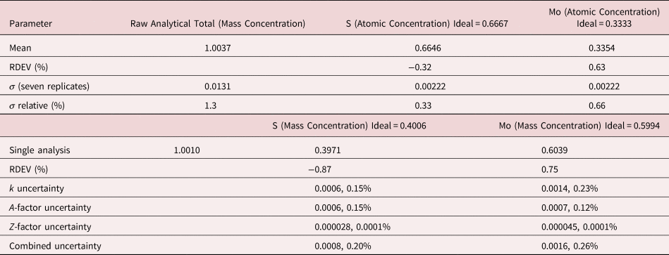
2. MoS2
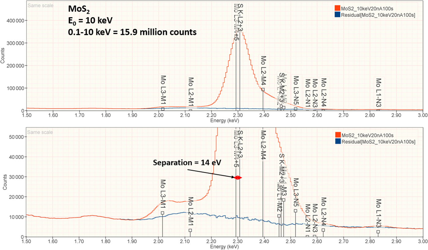
The analysis of MoS2 involves the interference of the S K-L2,3 at 2.307 keV and Mo L3-M4,5 at 2.293 keV, a separation of 14 eV at photon energy where the EDS resolution calculated with equation (6) is 88 eV, as shown in Figure 3. The NIST DTSA-II analysis of MoS2 at E 0 = 10 keV is given in Table 11 with concentrations expressed in atom fraction. RDEVs below 1% relative are obtained in this analysis.

Fig. 3. EDS spectrum of MoS2 (E 0 = 10 keV) showing the region of the S K-family and the Mo L-family; lower, the peak fitting residual spectrum (blue) after fitting for S and Mo.
Table 11. Analysis of MoS2 [E 0 = 10 keV; CuS and Mo Used as Fitting References (S K-L2,3 and Mo L3-M4,5) and as Standards; Values in Atom Concentration; Combined Uncertainties as Estimated from NIST DTSA-II].
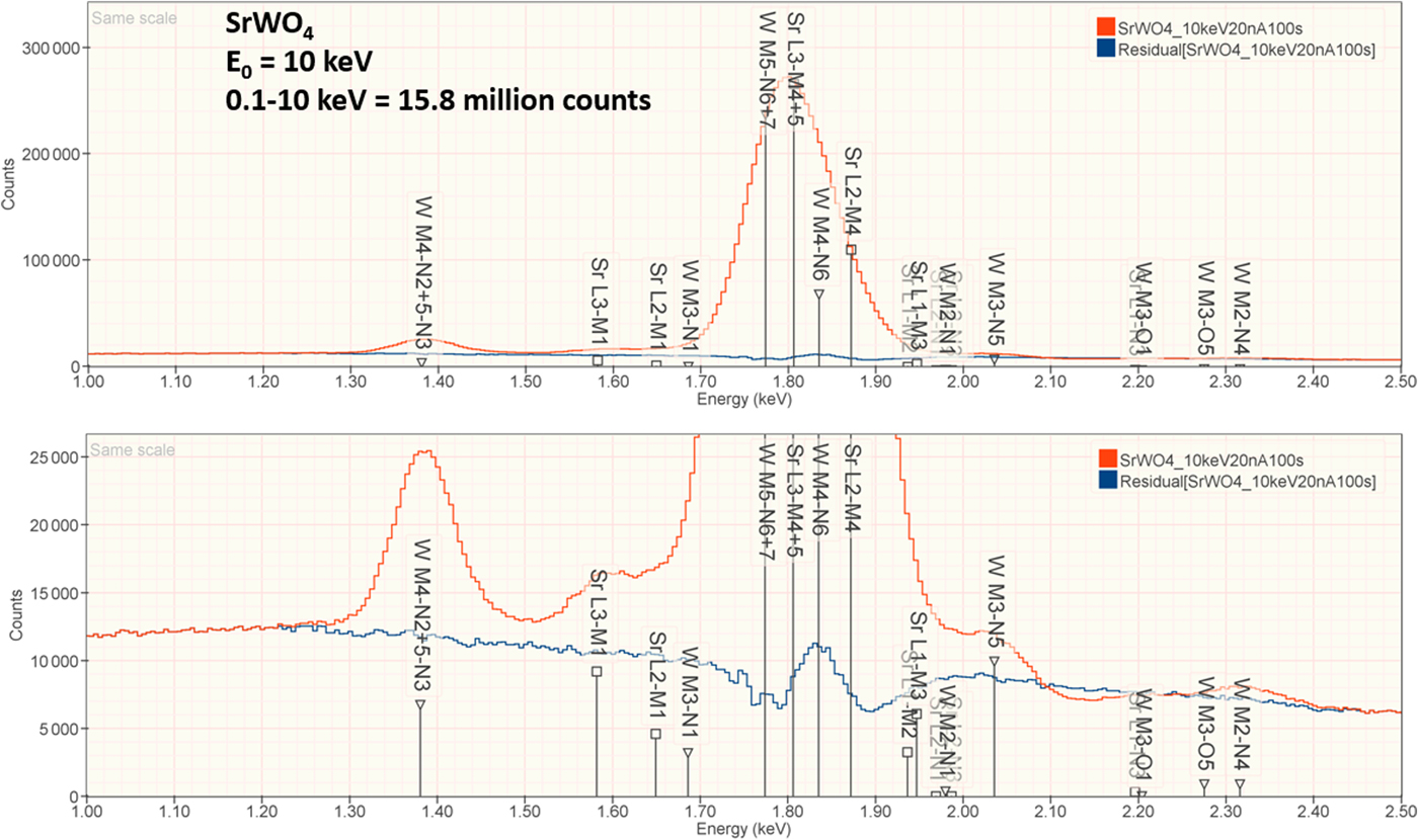
3. SrWO4
The analysis of SrWO4 involves the interference of a sequence of four peaks: W M5-N6,7 at 1.775 keV, which is separated by 31 eV from Sr L3-M4,5 at 1.806 keV, which is separated by 29 eV from W M4-N6 at 1.835 keV, which is separated by 37 eV from Sr L2-M4 at 1.872 keV at photon energy where the EDS resolution calculated with equation (6) is 79 eV, as shown in Figure 4. The NIST DTSA-II analysis of SrWO4 at E 0 = 10 keV is given in Table 12 with concentrations expressed in atom fraction. Oxygen was analyzed by employing the method of assumed stoichiometry. RDEVs below 1% relative are obtained in this analysis. Note that the peak-like structure found in the residual spectrum at 1.84 keV arises from the convolution of the sharp Si K-absorption step in the continuum background created during the passage of the X-rays through the dead-layer of the detector as well as the edges of the silicon support grid of the detector window.

Fig. 4. EDS spectrum of SrWO4 (E 0 = 10 keV) showing the region of the Sr L-family and the W M-family; lower, the peak fitting residual spectrum (blue) after fitting for Sr and W.
Table 12. Analysis of SrWO4 [E 0 = 10 keV; SrF2 and W Used as Fitting References (Sr L-family and W M-family) and as Standards; Oxygen Was Calculated by the Method of Assumed Stoichiometry; Values in Atom Concentration; Combined Uncertainties as Estimated from NIST DTSA-II].

4. Benitoite (BaTiSi3O9)
The analysis of the mineral Benitoite (BaTiSi3O9) involves the interference of the Ti K-L2,3 peak at 4.508 keV and Ba L3-M4,5 at 4.467 keV, a separation of 41 eV at photon energy where the EDS resolution calculated with equation (6) is 115 eV, as shown in Figure 5. The NIST DTSA-II analysis of Benitoite at E 0 = 10 keV is given in Table 13 with concentrations expressed in atom fraction. Oxygen was analyzed following the method of assumed stoichiometry. RDEVs below 1% relative, with the exception of Ba at 1.3%, are obtained in this analysis.
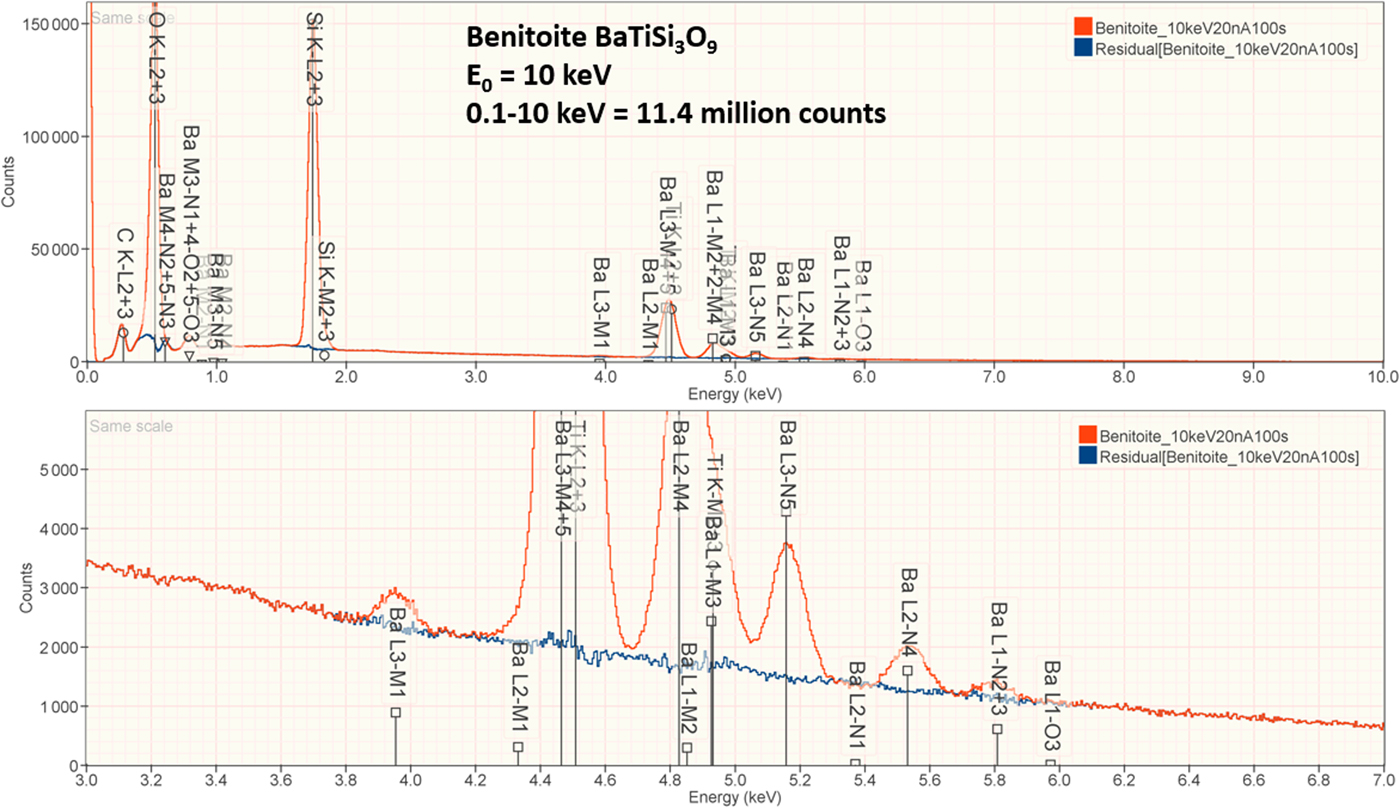
Fig. 5. EDS spectrum of the mineral Benitoite (BaTiSi3O9) (E 0 = 10 keV) showing the region of the Ti K-family and the Ba L-family; lower, the peak fitting residual spectrum (blue) after fitting for Ti and Ba.
Table 13. Analysis of Benitoite (BaTiSi3O9) [E 0 = 10 keV; Ti and Sanbornite (BaSi2O5) Used as Fitting References (Si K-family, Ti K-family, and Ba L-family) and as Standards; Oxygen Was Calculated by the Method of Assumed Stoichiometry; Values in Atom Concentration; Combined Uncertainties as Estimated from NIST DTSA-II].

Analysis with Peak Overlap and a Large Concentration Ratio between the Interfering Elements
When severe peak overlap occurs between two elements present at markedly different concentrations, the peak fitting problem becomes much more challenging. The Ti K-family and Ba L-family interference were used to test how well peak fitting of EDS spectra could match the direct separation of the interfering peaks by WDS for the measurement of k-ratios (Ritchie et al., Reference Ritchie, Newbury and Davis2012). The simultaneously measured EDS and WDS k-ratios are compared in Figure 6 for a range of Ba/Ti concentrations found in Benitoite, barium titanate, and various Ba–Ti–Si–O glasses listed in the inset table. Within the uncertainty of the counting statistics, the EDS k-ratios match the WDS k-ratios.
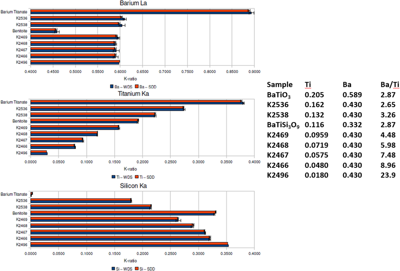
Fig. 6. Comparison of k-ratios measured by EDS (red) and WDS (blue) on Benitoite (BaTiSi3O9), BaTiO3, and a series of Si–Ti–Ba–O glasses. The Ti and Ba mass concentrations and the Ba/Ti concentration ratios are listed in the inset table.
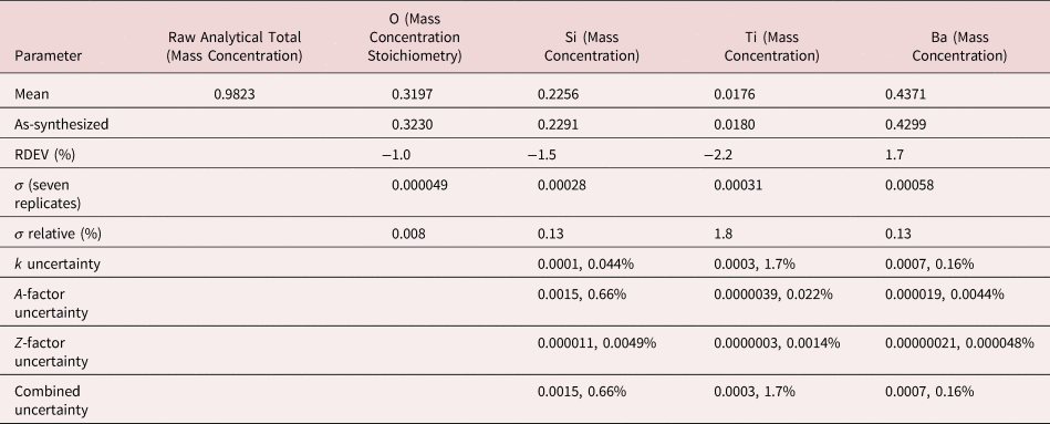
Figures 7a and 7b show the EDS spectrum of K2496, the glass with the most extreme Ba/Ti ratio in the series presented in Figure 6, and the peak fitting residual after fitting for both the Ti K-family and the Ba L-family. The NIST DTSA-II analysis results are given in Table 14 with concentrations expressed in mass fraction. Oxygen was analyzed following the method of assumed stoichiometry. Despite the severe interference and the large concentration ratio, the RDEV for Ti was −2.2%. For the major constituents, RDEV for Si was −1.5% and for Ba was 1.7%.
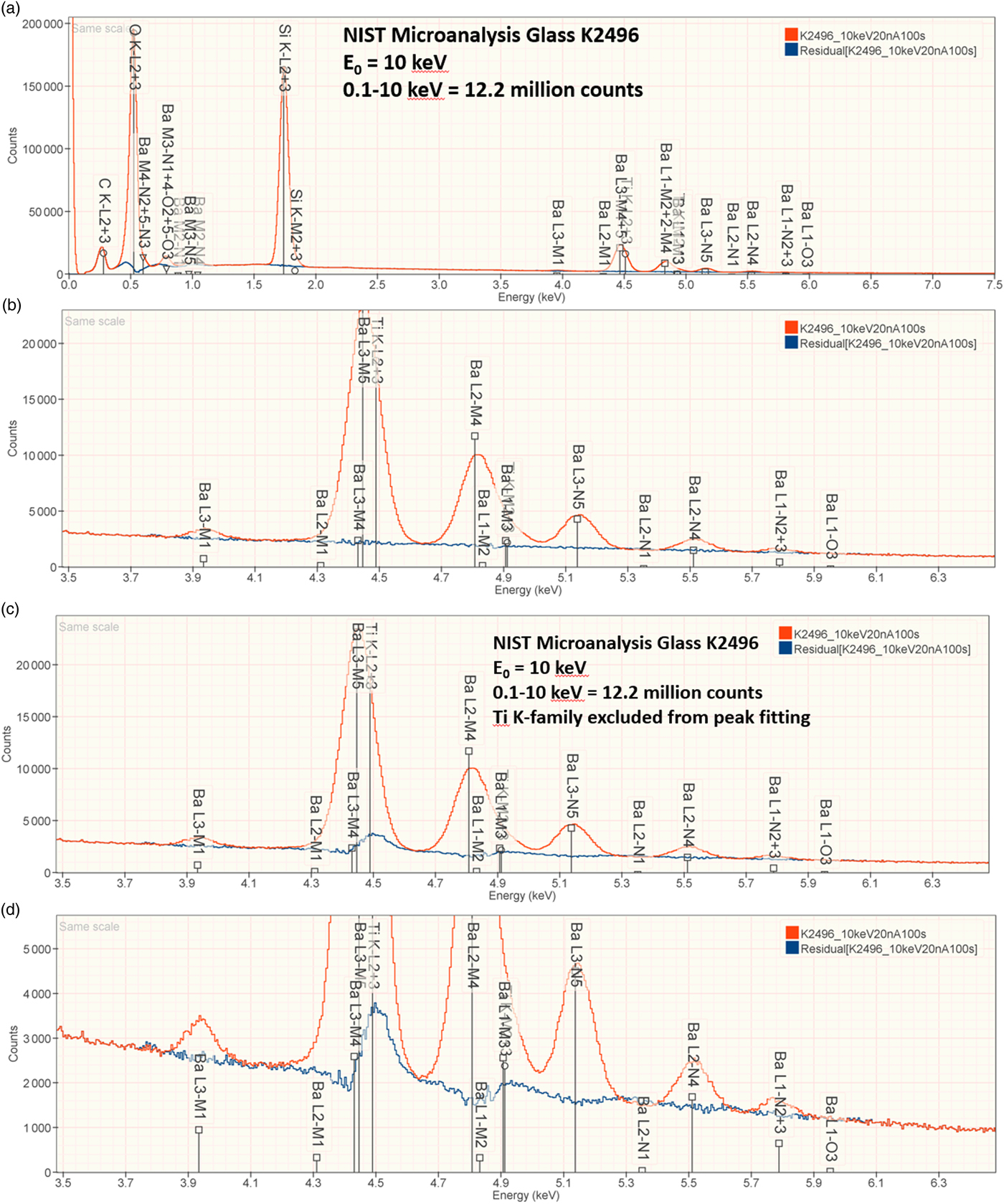
Fig. 7. EDS spectrum of NIST microanalysis glass K2496 (E 0 = 10 keV): (a) showing all constituents; (b) showing the region of the Ti K-family and the Ba L-family and the peak fitting residual (blue) after fitting for Ti and Ba; (c) showing the region of the Ti K-family and the Ba L-family and the peak fitting residual spectrum (blue) after fitting only for the Ba L-family; and (d) an expanded intensity axis.
Table 14. Analysis of NIST Microanalysis Glass K2496 [E 0 = 10 keV; Ti and Sanbornite (BaSi2O5) Used as Fitting References (Si K-family, Ti K-family, and Ba L-family) and as Standards; Oxygen Was Calculated by the Method of Assumed Stoichiometry; Values in Normalized Mass Concentration; Combined Uncertainties as Estimated from NIST DTSA-II].
A reasonable question to ask is whether the analyst would have detected the presence of the minor Ti constituent in the presence of the major Ba constituent if K2496 had been a true unknown. Indeed, because of the large concentration ratio of Ba/Ti = 23.9 in K2496, it would be highly likely that only the Ba L-family would have been assigned to the extended peak structure found in the region of 4.5 keV. Repeating the analysis with peak fitting only for the Ba L-family yields the peak fitting residual shown in Figure 7c and expanded in Figure 7d. The Ti K-family peaks are clearly visible so that a prudent analyst, upon inspecting the peak fitting residual spectrum, would repeat the analysis and include Ti in the suite of elements for analysis.
Iterative Qualitative–Quantitative Analysis to Discover Hidden Peaks
This example of NIST microanalysis glass K2496 illustrates the basis for a robust analytical strategy for EDS microanalysis in which qualitative and quantitative analyses with the construction of peak fitting residual spectrum are applied iteratively (Newbury & Ritchie, Reference Newbury and Ritchie2018). After each round of peak fitting, the residual spectrum is inspected to discover any previously unrecognized peaks and to assign them to the correct elements using the characteristic peak markers. Note that discontinuities in the continuum background caused by absorption edges and broadened by the detector function into peak-like structures can also be detected.
Additionally, when the standards-based intensity ratio protocol is applied for quantitative analysis, the raw (unnormalized) analytical total, which is the sum of all elemental concentrations including oxygen calculated by the method of assumed stoichiometry, is determined. As discussed above, deviations in the analytical total provide important information, especially a low total which should be considered as a possible indicator of a missing element(s).
An example of iterative qualitative–quantitative analysis is presented in Figure 8 and Table 15 for the analysis of NIST SRM 168, a Cr–Co–Ni “heat resisting alloy.” While the overall composition of this SRM is specified, it is not suitable as a microanalysis standard because of phase segregation on a microscopic level. The EDS spectrum of inclusion found in this microstructure, shown in Figure 8, reveals prominent peaks for Ta and Nb, and lower intensity peaks for C, Ti, Cr, Co, and Ni. When the standards-based quantitative analysis is performed for this suite of elements, the results given in Table 15 yield a raw analytical total of 0.9325 strongly suggesting that one or more elements have been overlooked. The first fitting residual, shown in Figures 8c and 8d, reveals the W M-family under the Ta M-family, including a sinusoidal structure at approximately 2.2 keV that may be related to nearby the W M-III absorption edge. Note also that structure remains in the region below 350 eV after fitting the C K-L peak, which may arise from the N-families of Ta and W, which are not included in the fitting references.
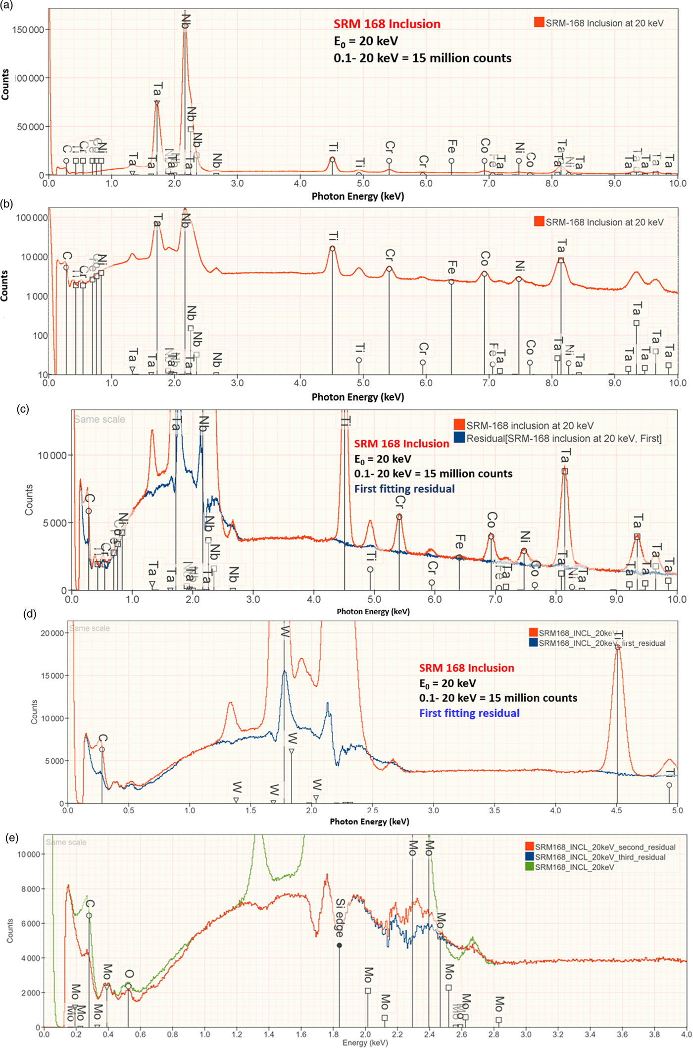
Fig. 8. EDS spectrum of an inclusion in NIST SRM 168 (E 0 = 20 keV) for the photon energy range from 0 to 10 keV: (a) full spectrum with a linear intensity axis; (b) full spectrum with a logarithmic intensity axis; (c) spectrum and peak fitting residual spectrum (blue) after fitting for Ti, Cr, Fe, Co, Nb, and Ta; (d) expansion 0–5 keV showing the detection of the W M-family in the peak fitting residual spectrum; and (e) original spectrum (green) and comparison of second (red) and third (blue) peak fitting residual spectra, showing the detection of Mo L-family. Note that where the red and blue traces overlap exactly, the red spectrum dominates the display.
Table 15. Analysis of an Inclusion in SRM 168 (E 0 = 20 keV) Pure Element Standards.

Including W in the suite of analyzed elements improves the peak fitting, also eliminating the sinusoidal feature at 2.2 keV, and increases the analytical total to 1.001, as given in Table 15. Inspection of the second fitting residual reveals the Mo L-family (Figure 8e) and upon including Mo in the suite of analyzed elements, the analytical total reaches 1.014. After fitting for Mo, the third residual shows no further peak structures in this region, as shown in Figure 8e. Additional counts in the spectrum of the unknown would be needed to examine the fitting residual for further trace constituents.
Analysis of Low Atomic Number Elements
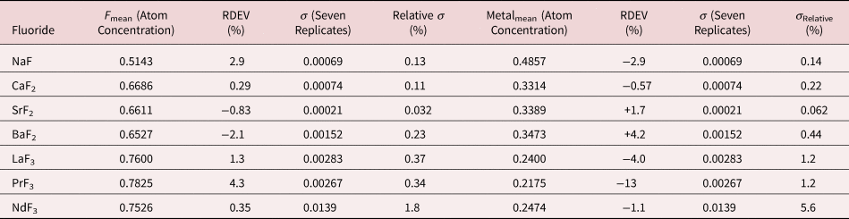
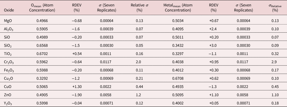
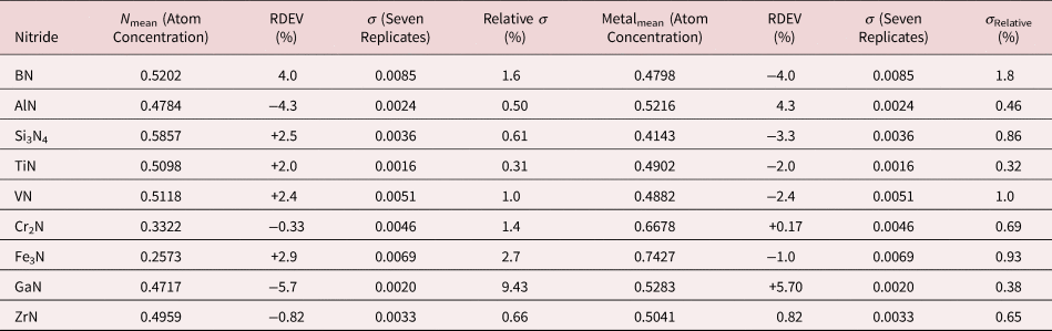
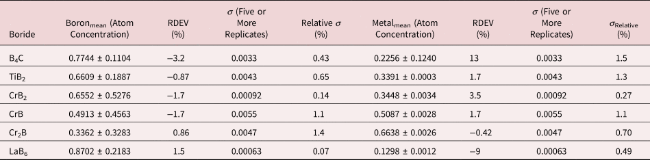
Because of the modest performance of the Si(Li)-EDS for photon energies below 1 keV and the strong self-absorption of low energy photons resulting in large absorption correction factors, quantitative analysis was considered problematic for low atomic number elements, Li–F, whose characteristic X-ray peaks fall in this photon energy range. The SDD-EDS has substantially improved performance for low-photon energies, especially when combined with the class of ultra-thin vacuum isolation windows now available, e.g., Si-grid-supported polymer and boron nitride, or in the windowless mode available for high vacuum instrument platforms. Moreover, improved models for the depth distribution of electron-induced ionization have resulted in more accurate absorption corrections in the low photon energy range. This combination of improved EDS spectrometry and improved absorption correction now enables accurate analysis of low atomic number elements, as presented in Tables 16 (fluorides), 17 (oxides), 18 (nitrides), 19 (carbides), and 20 (borides) (Newbury & Ritchie, Reference Newbury and Ritchie2015b). For these analyses, low (5 keV) to intermediate (10 keV) beam energies were chosen to minimize the strong effects of self-absorption of the low energy X-rays within the target. It is worth noting that most of the results in Tables 16–20 fall within ±5% RDEV. Note that as a consequence of the improved detector performance at low photon energy, greater attention will be required to measure and catalog the unfamiliar L-family, M-family, and N-family X-rays of the higher atomic number elements that occur in this energy region so that these peaks can be included in fitting, especially when these X-ray families impact the measurement of the low atomic number element K-families.
Table 16. Analysis of Binary Fluorides [All Analyses Performed with E 0 = 10 keV and the K-L2,3 Peak (Na and Ca), L3-M4,5 Peak (Sr, Ba, and La), M5-N6,7 (Pr and Nd)].

Table 17. Analysis of Binary Oxides (All Analyses Performed with E 0 = 10 keV and the K-L2,3 Peak, except for Zn L3-M4,5 and Y L3-M4,5).

Table 18. Analysis of Binary Nitrides [All Analyses Performed with E 0 = 5 keV (ZrN at 10 keV); K-L2,3 Peak for B, Al, and Si; All others L-Family].

Table 19. Analysis of Binary Carbides [Analyses Performed with the K-L2,3 Peak (E 0 = 10 keV) or L-Family for Hf (E 0 = 5 keV)].
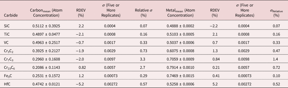
Table 20. Analysis of Binary Borides (All Analyses Performed with E 0 = 5 keV; B K-L2,3 Peak, C K-L2,3 Peak, Ti and Cr L-Family, and La M-Family Peaks).

Analysis at Low Beam Energy
The electron range decreases rapidly as the incident beam energy, E 0, is reduced, with a functional dependence of  $E_0^{1.67}$, improving the lateral resolution and reducing the sampling depth (Goldstein et al., Reference Goldstein, Newbury, Michael, Ritchie, Scott and Joy2018). However, to excite a particular characteristic X-ray peak, the beam energy must exceed the critical shell excitation energy, E c, ideally by a factor of at least 1.25. This condition places practical constraints on the selection of E 0. A beam energy of 5 keV is the lowest value at which at least one characteristic X-ray peak or family can be excited for all elements of the Periodic Table, except for H and He which do not produce characteristic X-rays. As the beam energy is reduced below 5 keV, an increasing number of elements becomes inaccessible to EPMAdue to the lack of a practically measurable characteristic X-ray peak (Newbury & Ritchie, Reference Newbury and Ritchie2016a). Even with the selection of E 0 = 5 keV, the analyst is forced to make use of unfamiliar X-ray families for some elements. For example, Ba is typically analyzed with the Ba L-family X-rays (L3 = 5.247 keV), but this family is not available with E 0 ≤ 5 keV, requiring the use of the Ba M-family, which is illustrated in Figure 9a. A difficult low beam energy analysis involving the Ba M-family is presented in Figure 9b, which shows the spectrum for YBa2Cu3O7 and the peak-fitting residual. This analysis involves interference of the O K-L2,3 family and the Cu L-M family with the Ba M-family. The results, including oxygen analyzed with a standard, are presented in Table 21, where the largest RDEV is 6.5% relative for Y. Ba, despite the severe interference of the O K-L2,3 family and the Cu L-M family, is analyzed with an RDEV of 0.5%. Additional challenges that become significant at low beam energy include the stratified nature of most materials. Native oxides and other surface layers make a more significant contribution to the measured spectrum at low incident beam energy compared with the measurement at conventional beam energies, where the surface layer comprises only a small fraction of the total electron range. Contamination from carbon deposition can increase the absorption of X-rays with energies near the carbon K-edge (0.284 keV) above that expected from the compositions of the unknown and standard. While this effect also occurs for conventional beam energy analysis, the analytical strategy can usually make use of more energetic characteristic X-ray peaks that are much less affected by absorption from the contamination layer.
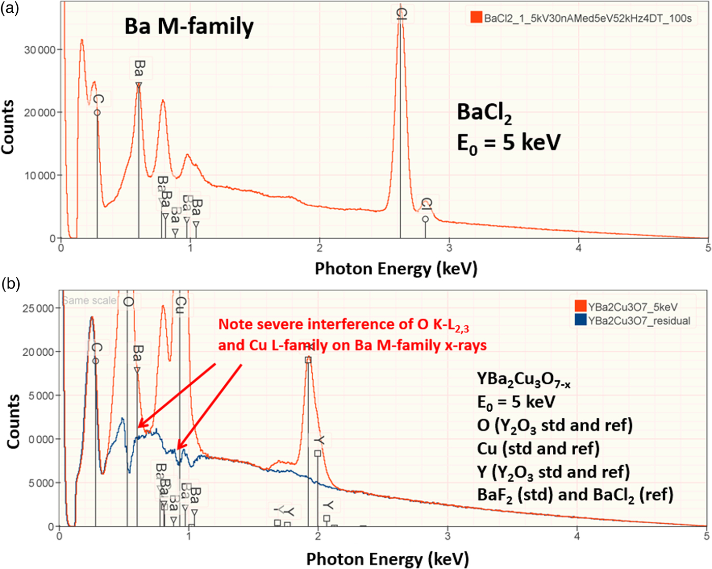
Fig. 9. (a) EDS spectrum of BaCl2 at E 0 = 5 keV; note the extended Ba M-family. (b) EDS spectrum (red) of YBa2Cu3O7−x at E 0 = 5 keV and the peak fitting residual spectrum (blue).
Table 21. Analysis of YBa2Cu3O7 at E 0 = 5 keV. O (Y2O3 Standard and Reference); Cu (Standard and Reference); Y (Y2O3 Standard and Reference); Ba (BaF2 Standard and BaCl2 Reference), Values in Normalized Mass Concentration; Combined Uncertainties as Estimated from NIST DTSA-II.

Microanalysis of Trace Elements
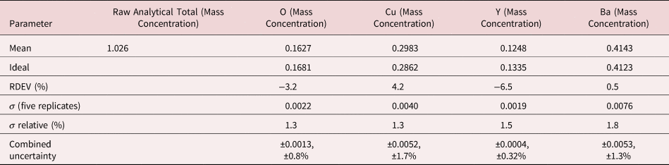
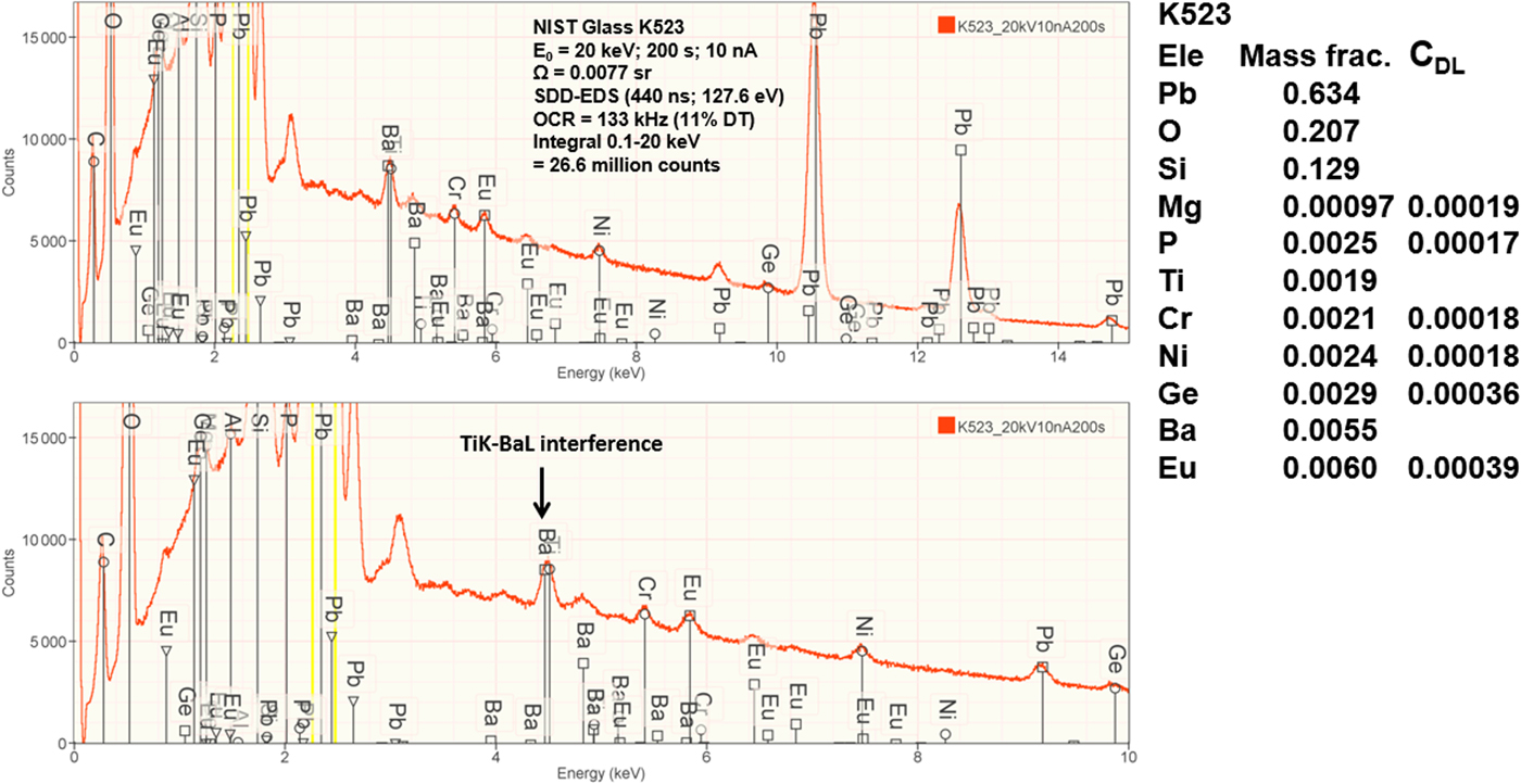
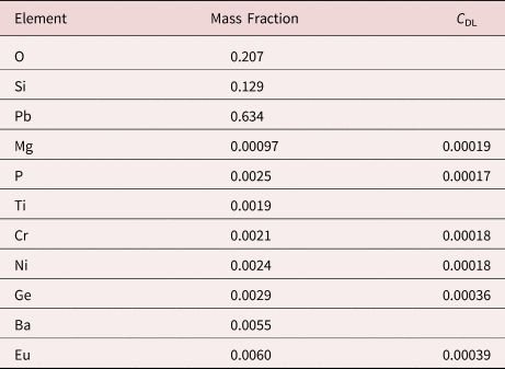
Measurement of trace elements, arbitrarily defined in this paper as those present at a mass concentration C < 0.01, involves fitting peaks that are close to the X-ray continuum background and that may also be subject to overlap from the significantly more intense peaks of major and minor constituents. In the absence of significant peak overlap, limits of detection in the range 0.0002–0.0005 mass concentration (200–500 parts per million), depending on the particular element and the matrix composition, can be reached with counting times below 500 s (Newbury & Ritchie, Reference Newbury and Ritchie2016b). An example is shown in Figure 10 for NIST microanalysis glass K523, which has the as-synthesized composition listed in Table 22. For peaks that do not suffer interference, C DL, the limit of detection (minimum mass fraction) can be estimated from the measured (or independently known) composition as
 $$C_{{\rm DL}} = [3N_\rm B^{1/2} /\lpar {{\it N}_{\rm S} - {\it N}_{\rm B}} \rpar ]{\it C}_{\rm S},$$
where N B is the number of counts in the background under the peak (integral across the contiguous channels that define the peak), N S is the number of counts in the peak integral, and C S is the known (or measured) concentration of the trace constituent (Goldstein et al., Reference Goldstein, Newbury, Michael, Ritchie, Scott and Joy2018). For the particular measurement conditions listed in Table 22, the values of C DL estimated with equation (6) are listed for several of the trace constituents.

Fig. 10. EDS spectrum of NIST microanalysis glass K523 (E 0 = 20 keV): upper, 0–15 keV; lower, 0–10 keV with an expanded intensity axis.
Table 22. NIST Microanalysis Glass K523 (E 0 = 20 keV; Integrated Counts 0.1 – 20 keV = 26.6 million).
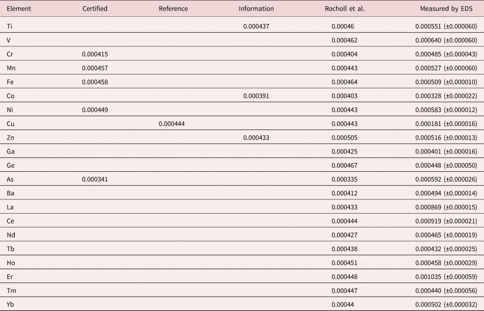
An example of trace measurements at the extreme limit of EDS microanalysis (spectrum integral 0.1–20 keV = 1.7 billion counts) is presented in Figure 11, which shows the spectrum of NIST SRM 610 (“Trace Elements in Glass”) containing numerous trace elements at a nominal level of 0.0005 mass fraction (500 parts per million) in a matrix of O–Na–Al–Si–Ca. There are many peak interference situations encountered in the analysis of SRM 610, but those that involve mutual interferences of trace constituents that produce peaks of similar intensity, e.g., the Ti K-family and the Ba L-family, can be solved with peak fitting. Table 23 gives the results of the DTSA-II analysis. With some exceptions, e.g., Cu, the EDS results are consistent with the bulk analysis values reported for this SRM (Newbury & Ritchie, Reference Newbury and Ritchie2016b).
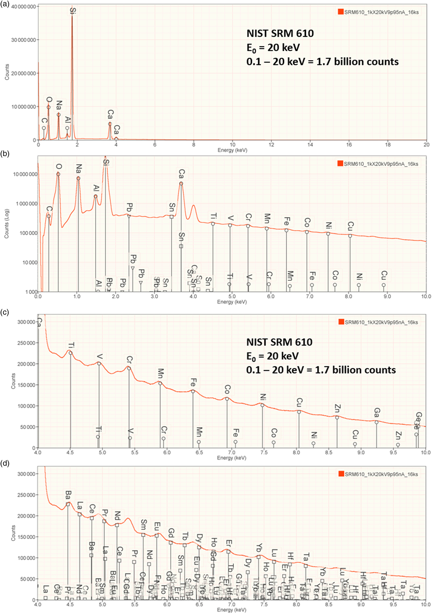
Fig. 11. EDS spectrum of NIST trace elements in glass SRM 610 (E 0 = 20 keV): (a) 0–20 keV, full spectrum, linear axis; (b) 0–10 keV with a logarithmic intensity axis; (c) 4–10 keV, peak labels for transition metals; and (d) 4–10 keV, peak labels for Ba, rare earth elements, Hf, Ta.
Table 23. Analysis of NIST SRM 610 (Trace Elements in Glass) (E 0 = 20 keV; Integrated Counts 0.1–20 keV = 1.7 billion).
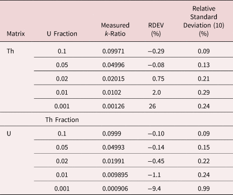
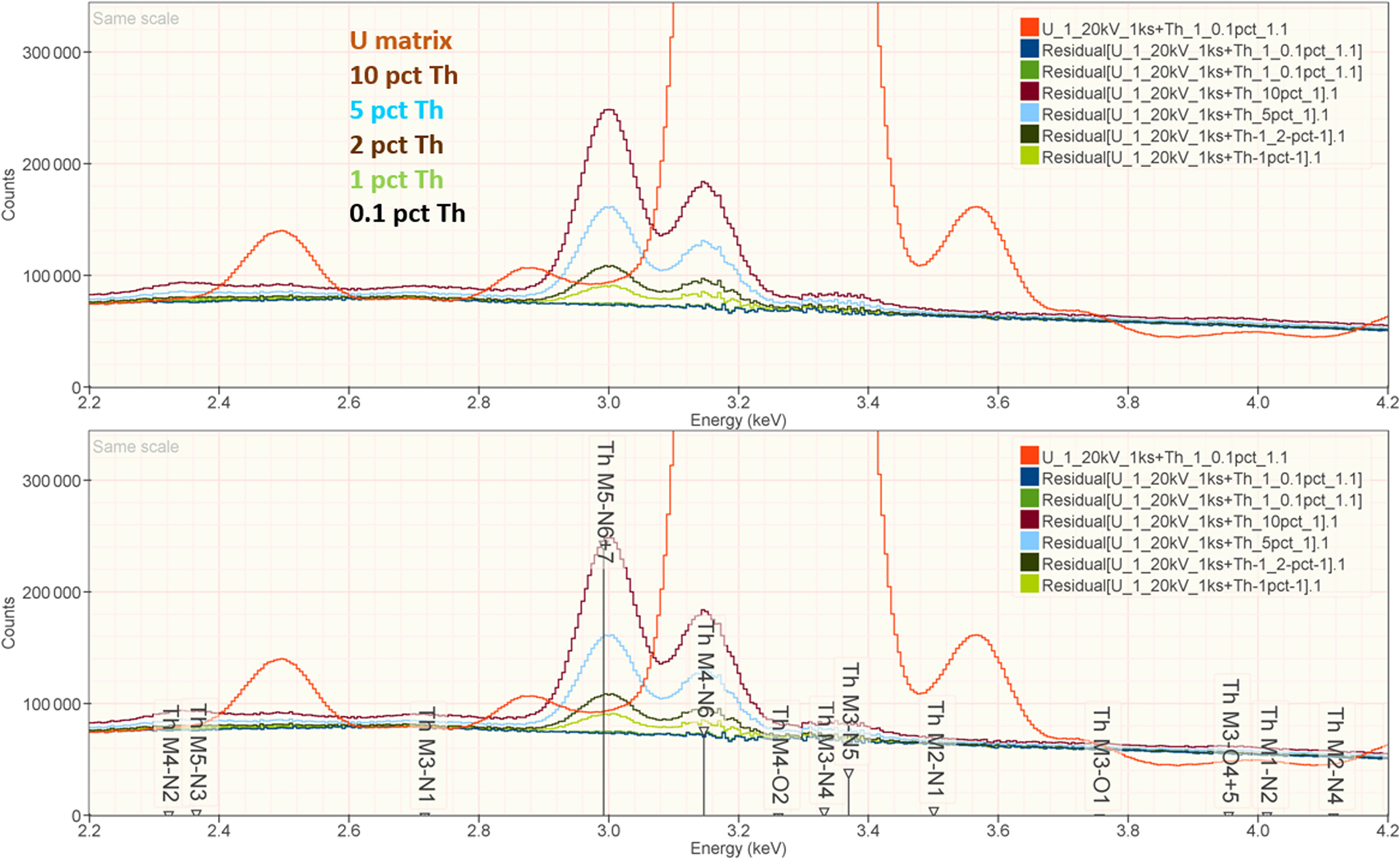
When the X-ray peak for a trace constituent is buried under the interfering peak of a major or minor constituent, the measurement challenge is substantially increased. Moreover, there are relatively few materials of known composition with such major/minor interferences on trace constituents that can serve as unknowns to test the performance of peak fitting in such situations. As an alternative, the “spectrum arithmetic” tools in NIST DTSA-II can be used to create suitable synthesized composite spectra from experimentally measured spectra. The synthesized spectra are then subjected to peak fitting using different experimentally measured spectra as peak references. Examples of such studies are presented in Table 24 for the interference of the Th M-family and the U M-family for which Th M4-N6 (3.146 keV) and U M5-N6,7 (3.165 keV) families are separated by 19 eV at photon energy where the EDS resolution is 99 eV. For an intensity ratio of 100:1, the k-ratio for the trace constituent is recovered with an RDEV of 2% for U in a Th-matrix and −1.1% for Th in a U-matrix. When the relative intensity ratio is increased to 1,000:1, the k-ratio for the trace constituent is recovered with an RDEV of 26% for U in a Th-matrix and −9.4% for Th in a U-matrix. Figure 12 shows the spectra for the U-matrix with Th additions. When Th is not included in the peak fitting suite, the peak fitting residual spectra visually reveal the Th constituent down to the 1% level. Figure 13 shows the same sequence for the Th-matrix with U additions, and again when U is not included in the peak fitting suite, the peak fitting residual spectra visually reveal the U constituent down to the 1% level.
Table 24. Peak Fitting Results for Th–U Synthesized Spectra; Original Spectra: Th M-Family 63,004,000 Counts; U M-Family 58,282,000 Counts.


Fig. 12. EDS spectrum of U-matrix with Th additions composed with spectrum tools in NIST DTSA-II from experimentally measured spectra for U and Th (E 0 = 20 keV); the peak fitting residual spectra are shown for fitting only with U.

Fig. 13. EDS spectrum of Th-matrix with U additions composed with spectrum tools in NIST DTSA-II from experimentally measured spectra for U and Th (E 0 = 20 keV); the peak fitting residual spectra are shown for fitting only with Th.
“Standardless” Analysis
“Standardless” analysis avoids the need to measure a standard intensity for the denominator of the k-ratio in equation (4) either by calculating an intensity from the equations of X-ray generation and propagation (“first-principles” method) or by using a library of remotely measured standards (“remote standards” method) (Goldstein et al., Reference Goldstein, Newbury, Michael, Ritchie, Scott and Joy2018). The accuracy of the first-principles method is limited by the lack of accurate values for critical physical parameters such as the ionization cross section and the fluorescence yield, especially for L- and M-shell X-rays. Since the remote standards method is tied to measurements of real materials, it is inherently more accurate and is a good compromise between first-principles standardless analysis and locally collected standards-based analysis. However, the user is often left guessing how vendors implement their “standard-less quantification” because they have typically not provided the customer with adequate documentation on what is actually being done to derive numerical concentrations.
The remote standards library is populated with characteristic X-ray peak intensities from the pure element and stochiometric compounds measured at several beam energies with a carefully characterized EDS. If a given analysis requires a standard not in the library or at a beam energy not represented, then interpolation/extrapolation from existing measurements augmented by the equations of X-ray generation and propagation can be used to supply the missing value(s). Finally, the difference in the relative efficiencies of the reference EDS and the local EDS at the photon energy of each elemental intensity must be corrected. One method is to use a “golden detector” calibrated at a beamline and a carefully chosen reference material to transfer the calibration from the golden detector to others (Alvisi et al., Reference Alvisi, Blome, Griepentrog, Hodoroaba, Karduck, Mostert, Nacucchi, Procop, Rohde, Scholze, Statham, Terborg and Thiot2006).
Standardless analysis requires only that the analyst provides the beam energy and the X-ray spectrometer takeoff angle relative to the specimen surface. Knowledge of the electron dose is not needed. However, the loss of the dose information means that standardless analysis results, including oxygen if calculated by the method of assumed stoichiometry, must be normalized to unity mass fraction (100 wt%) to be placed on a sensible basis. Standardless analysis methods that incorporate the known dose of the remote reference spectrum (e.g., Cu) or which are based on peak-to-background measurements can recover a meaningful raw analytical total.
Early testing of standardless analysis with known materials revealed a distribution of RDEVs such that 95% of the analytical results spanned an RDEV range of ±25% relative (Newbury et al., Reference Newbury, Swyt and Myklebust1995). A more recent study produced similarly broad RDEV results, as shown in Figure 14 (Ritchie & Newbury, Reference Ritchie and Newbury2014). Such a test of an individual vendor's standardless analysis procedure obviously does not represent a rigorous examination of all available software, and indeed vendor software undergoes a frequent change, creating a moving target. However, it is interesting to note that customers are not typically provided by the vendor with rigorous testing of the accuracy of the standardless analysis procedure that would include analysis of certified reference materials and stoichiometric compounds in the conventional beam energy range, at low beam energy, and of elements that can only be analyzed with low energy photon peaks. The availability of results on such a test suite would make an excellent customer request!

Fig. 14. RDEV histogram constructed with results of a vendor standardless analysis procedure applied to known materials.
The vast majority of EDS quantitative compositional results are likely being derived from standardless analysis, perhaps 95% or more! While improvement in the accuracy of the standardless method is certainly possible and highly desirable, it must be recognized that the ease of use of standardless analysis currently comes at the likely expense of a significant reduction in accuracy compared with the standards-based k-ratio protocol, if the RDEV distribution in Figure 14 is at all representative. Unless the vendor is willing to share a record of the analytical performance of the standardless analysis software, it is currently left up to the customer to test the software on known materials similar to what she/he wishes to analyze and under the beam conditions that are to be used.
Elemental Mapping
Elemental mapping with electron-excited X-ray spectrometry (WDS) was established by Cosslett & Duncumb (Reference Cosslett and Duncumb1956) and quickly became a powerful and popular method of studying compositionally heterogeneous microstructures. With the advent of EDS, especially with its immediate incorporation in the scanning electron microscope, mapping of specific elements with the X-ray signal became an important SEM imaging mode. In the SEM, elemental X-ray mapping complemented compositional imaging with the backscattered electron signal, which depends on the average atomic number but which is not element specific. The limited throughput of early EDS systems meant that the practical application of elemental mapping was mostly restricted to major constituents. Moreover, the dependence of the X-ray continuum background on the average atomic number meant that EDS elemental mapping using the total intensity (characteristic and continuum) within a peak-region-of-interest was increasingly subject to artifacts as the concentration of a constituent decreased into the minor and trace levels. Eliminating or at least minimizing such artifacts has been accomplished by the method of “X-ray spectrum imaging (XSI).” In XSI, the entire EDS spectrum is recorded at each picture element (pixel) of an imaging scan. Each pixel spectrum can be processed with quantitative corrections (standards-based or standardless) to achieve compositional mapping in which the gray or color level of a pixel is directly related to the concentration of an element. The limited throughput of the Si(Li)-EDS technology meant that XSI compositional mapping was effectively restricted to small pixel densities (e.g., 128 × 128) and long accumulation times extending to several hours to record adequate X-ray counting statistics in the single pixel spectrum. The great increase in throughput that has been achieved with SDD-EDS has made XSI compositional mapping much more time efficient and effective.
1. “Fast mapping” (<10 s): major constituents
The high SDD-EDS throughput, with an OCR of 100 kHz to 1 MHz or even greater possible with multiple SDD arrays, means that XSI mapping can gather useful information on major constituents in 10 s or less. This short accumulation time (“fast mapping”) approaches the speed of SEM-BSE imaging while retaining the element-specific capability of EDS. An application of fast mapping to the major constituents of a leaded-brass particle is shown in Figure 15 for a 640 × 480 pixel scan recorded in 5 s with an average throughput of 700 kHz with post-processing to correct for background contributions. The gray-level range of these fast maps is severely limited by the individual pixel-integrated spectrum count (10–100) and can only reveal the most abundant species present. Nevertheless, by using the method of the primary color overlay with Cu (red) Pb (green) Zn (blue), the localization of the Pb-rich inclusion is readily discernible, and though weaker, in contrast, redder regions that are slightly richer in Cu can be seen throughout the particle. Moreover, the color overlay also reveals unexpected dark regions within the particle boundaries. The derived “sum spectrum” shown in Figure 16, created by adding all the pixel spectra on a channel-by-channel basis, reveals the presence of an unexpected Ni K-L2,3 peak. When the map for Ni K-L2,3 is extracted from the XSI, Ni is found to fill in the empty regions seen in Figure 15, as shown in the color overlay with Cu (red), Ni (green) and Zn (blue) in Figure 17.
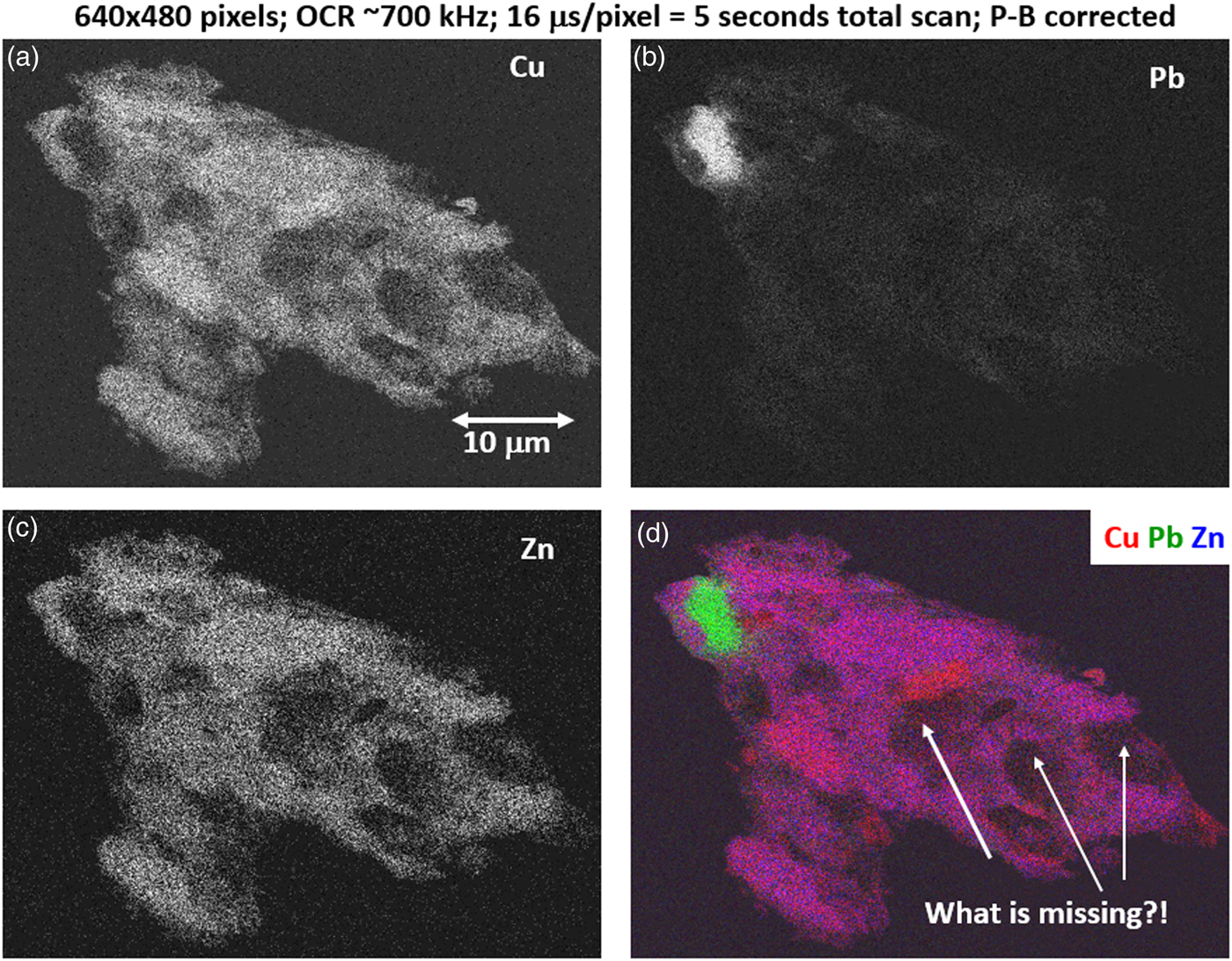
Fig. 15. Region-of-interest intensity maps for an X-ray spectrum image of a leaded-brass particle (E 0 = 20 keV). (a) Cu K-L2,3; (b) Pb M-family; (c) Zn K-L2,3; and (d) color overlay with Cu (red) Pb (green) Zn (blue); note the dark regions within the particle. (640 × 480 pixels; 16 µs/pixel; 5 s total frame time).

Fig. 16. Derived SUM spectrum calculated by adding all of the individual pixel spectra together; note the detection of Ni (red).
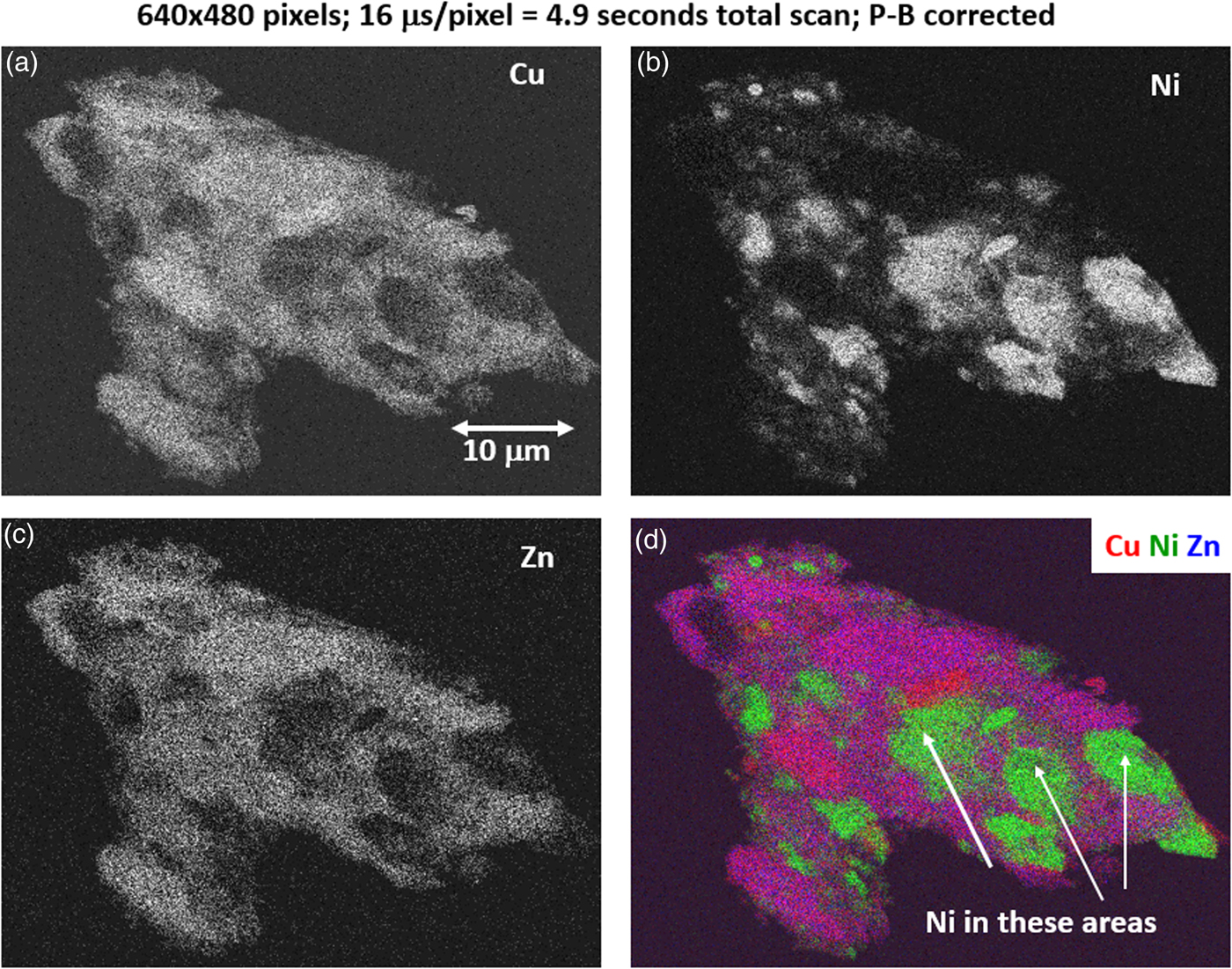
Fig. 17. Region-of-interest intensity maps for an X-ray spectrum image of a leaded-brass particle (E 0 = 20 keV). (a) Cu K-L2,3; (b) Ni K-L2,3; (c) Zn K-L2,3; and (d) color overlay with Cu (red) Ni (green) Zn (blue); note that the dark regions within the particle seen in Figure 14 are found to be filled with Ni. (640 × 480 pixels; 16 µs/pixel; 5 s total frame time).
2. Mapping with a deeper gray scale (10–100 s)
With an OCR of 100–1 MHz, extending the accumulation to the range 10–100 s can enable access to minor constituents in the XSI. For the example of Figure 15, by increasing the accumulation time by a factor of 16 (80 s), a deeper gray-level scale can be achieved, as shown in Figure 18 for the Cu and Ni images. Figure 18 also includes the SEM-BSE image with a large, symmetric two-segment BSE detector operating in the SUM mode, making it sensitive to BSE compositional contrast. Although much less noisy than the fast X-ray maps, the SEM-BSE image cannot be used to distinguish the Ni-rich regions from the Cu- and Zn-rich regions. A difference of approximately one unit of atomic number, e.g., Ni versus the Cu–Zn mixture, produces an insufficient compositional contrast in the BSE signal, which is further complicated by the superimposed topographic contrast due to surface roughness. Minor elements that can be recognized in the SUM spectrum of Figure 16 include Ca and Ti. Using the 80 s XSI, the elemental maps for Ca and Ti are extracted in Figure 19 and shown as a color overlay with Ti (red), Ca (green), and Zn (blue), revealing surface decoration.
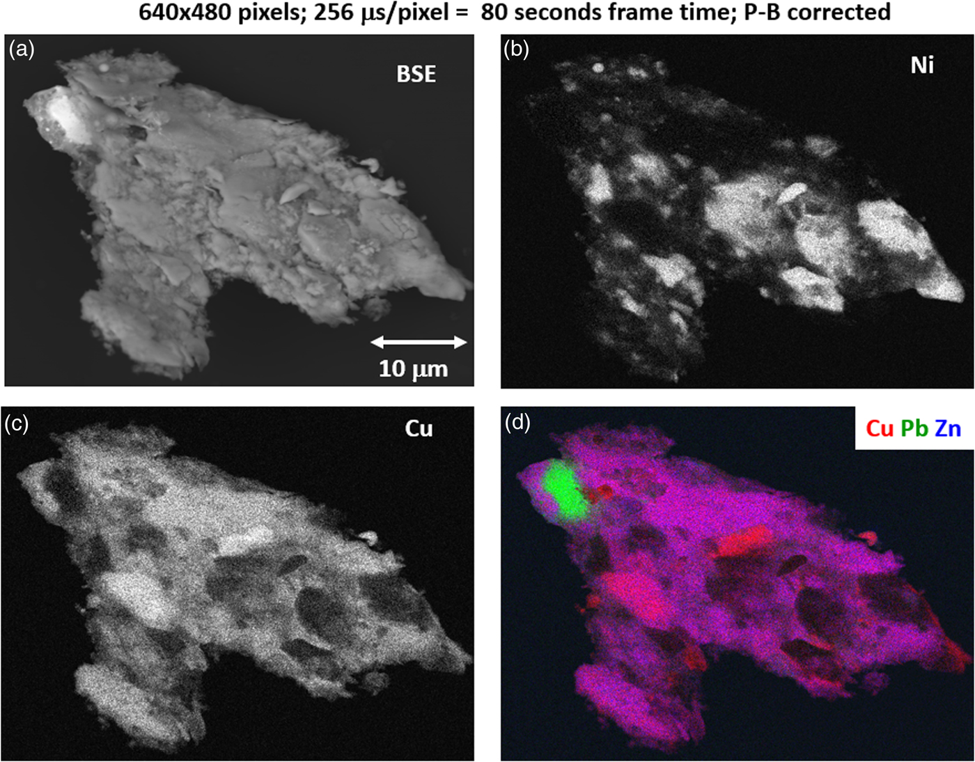
Fig. 18. (a) SEM-BSE image; region-of-interest intensity maps for an X-ray spectrum image of a leaded-brass particle (E 0 = 20 keV); (b) Ni K-L2,3; (c) Cu K-L2,3; and (d) color overlay with Cu (red) Ni (green) Zn (blue); note the deeper gray levels in each image. (640 × 480 pixels; 256 µs/pixel; 80 s total frame time).
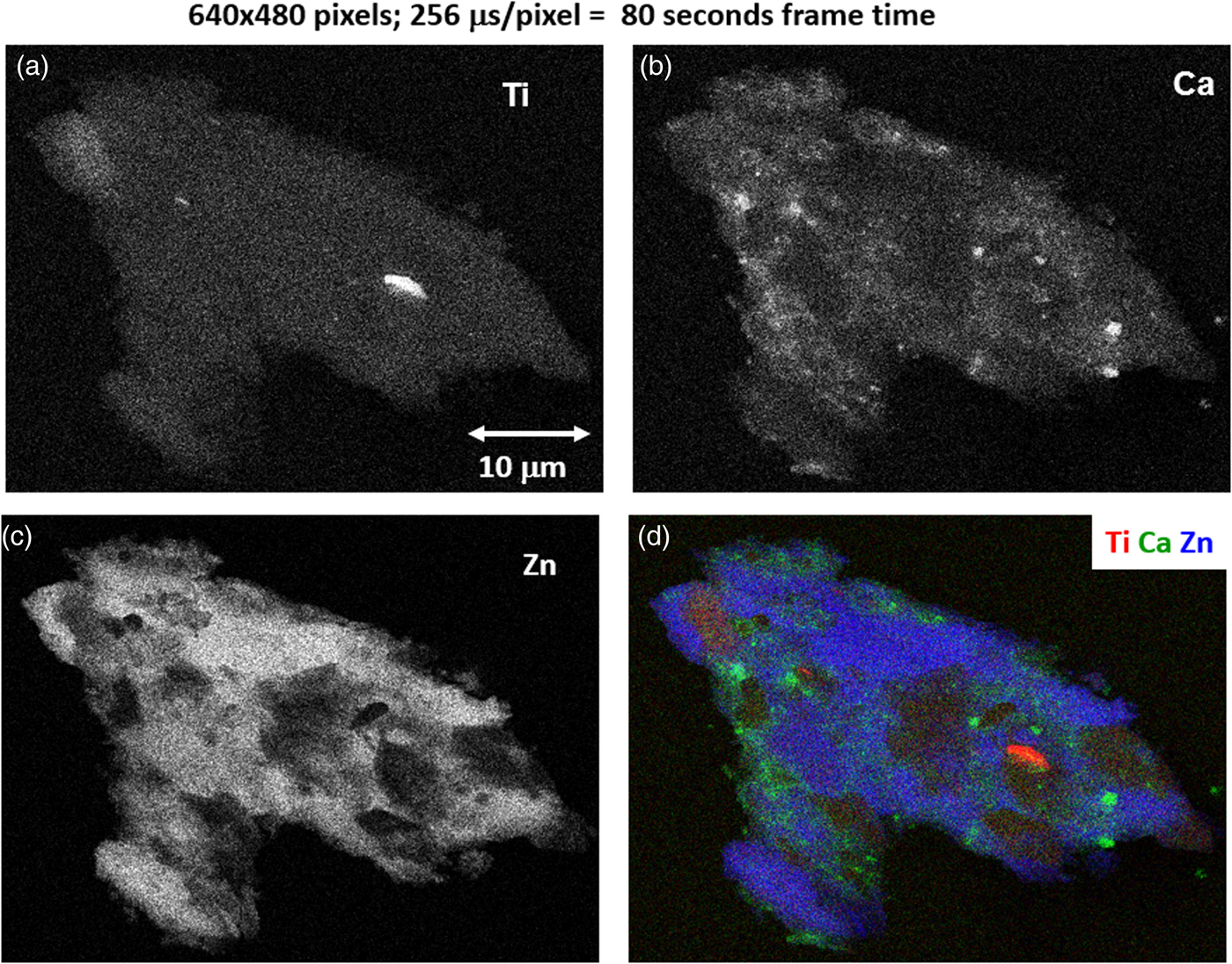
Fig. 19. Region-of-interest intensity maps for an X-ray spectrum image of a leaded-brass particle (E 0 = 20 keV). (a) Ti K-L2,3; (b) Ca K-L2,3; (c) Zn K-L2,3; and (d) color overlay with Ti (red) Ca (green) Zn (blue); (640 × 480 pixels; 256 µs/pixel; 80 s total frame time).
3. Compositional mapping (100–10,000 s)
The quantitative processing of individual pixel spectra for compositional mapping can be applied to any XSI, but achieving low variance elemental maps requires higher spectral counts, e.g., 1,000 or more counts per pixel spectrum. Depending on the map pixel density and the OCR, reaching this counting threshold may require 100–10,000 s. Figure 20 shows an example of region-of-interest total intensity maps of Al, Fe, and Ni derived from an XSI of Raney nickel alloy. For an XSI of 512 × 384 pixels, 3.2 ms/pixel (6,440 s) at an OCR of 450 kHz, the pixel spectra contain from 1,000 to 1,500 counts depending on the local composition. The traditional gray scale encoding of the raw intensity maps shown in Figure 20 imposes constraints on interpretation. To maximize the contrast within a given map, the intensity range has been scaled (“autoscaling”) to span the full gray scale range, from near black to near white. Thus, when considering the three elemental maps in Figure 20, near white corresponds to 0.995 mass fraction for the Al image, 0.535 for the Ni image, but only 0.042 for the Fe image. While useful for visualizing features within a single image and making useful relative comparisons within an image, autoscaling prevents sensible comparisons of the relative concentration among different elemental images or even for the same element from different areas of the same specimen if the concentration range differs between those areas. Figure 21 shows the same XSI data after standards-based quantitative processing to produce true compositional images. The concentration for each element is displayed with the “logarithmic three-band” encoding scheme: a major constituent (concentration 0.1 mass fraction to unity) is displayed with a band ranging from deep red to pink; a minor constituent (0.01–0.1 mass fraction) is displayed ranging from deep green to green pastel; and a trace constituent (0.001–0.01 mass fraction) is displayed ranging from deep blue to blue pastel (Newbury & Bright, Reference Newbury and Bright1999). This consistent encoding of quantitative concentration data with color bands that immediately distinguish “major,” “minor,” and “trace” constituents makes it possible to make sensible comparisons of different elements within a mapped area or between maps of the same element from different areas. Another advantage of quantitative compositional mapping and display with the log three-band encoding can be seen by comparing the Fe maps in Figures 20 and 21. In the raw intensity map of Fe shown in Figure 20, there appears to be a significant increase in the concentration of Fe in the Ni-rich region of the microstructure compared with the Al-rich region, but this compositional contrast is actually an artifact that results from the dependence of the X-ray continuum on the average atomic number of the material. The Fe content thus appears to be higher in the Ni-rich phases compared with the Al-rich phase. In the quantitative compositional map of Figure 21, this false contrast is substantially diminished, and Fe is seen to be a trace level everywhere except in the Fe-containing phase where its level rises to the level of a minor constituent.
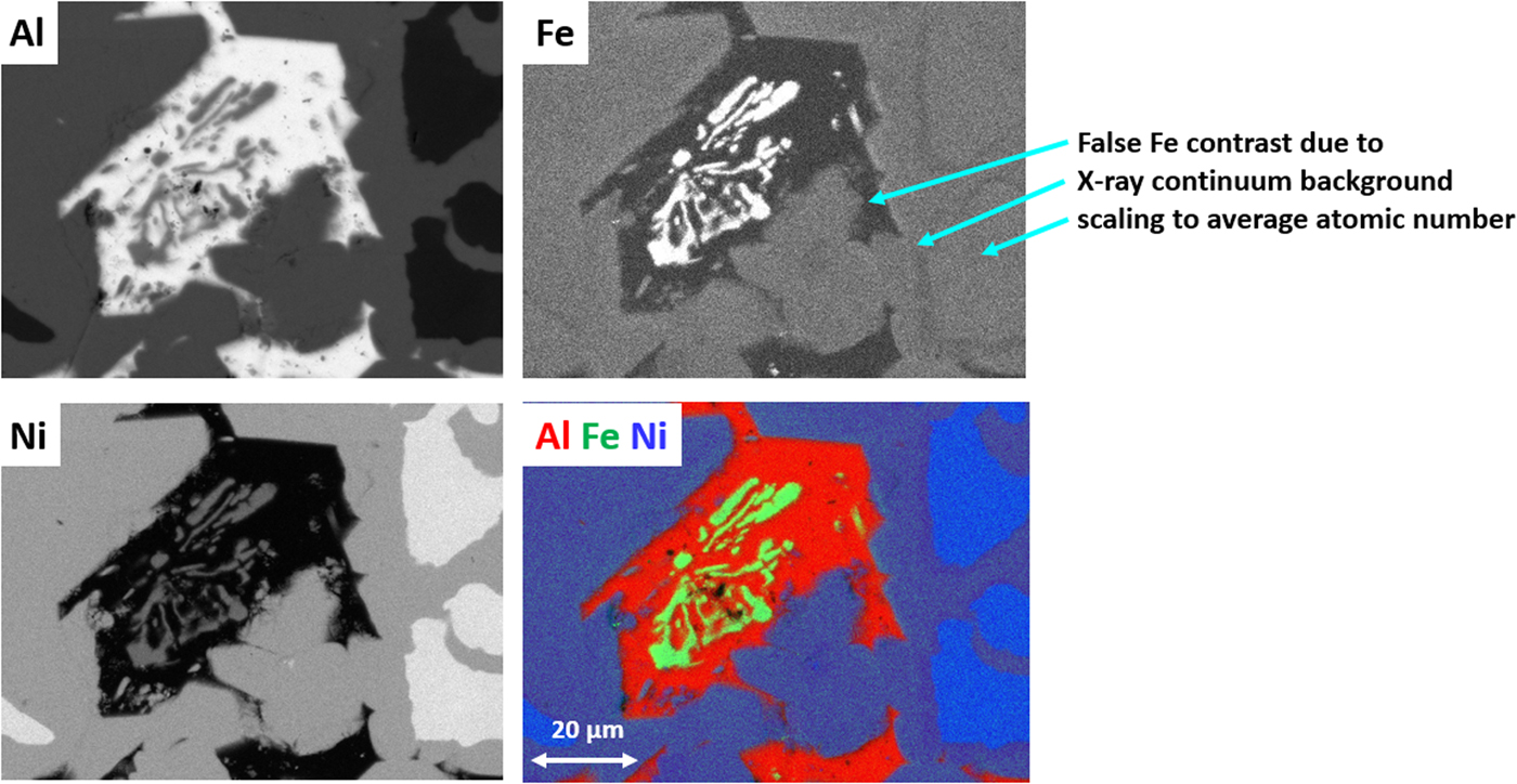
Fig. 20. Raney nickel alloy (E 0 = 20 keV; 512 × 384 pixels; 3.28 ms/pixel; 6,400 s/frame); raw intensity maps for Al, Fe, and Ni, and color overlay with Al (red) Fe (green) Ni (blue); note the false contrast in the Fe image.
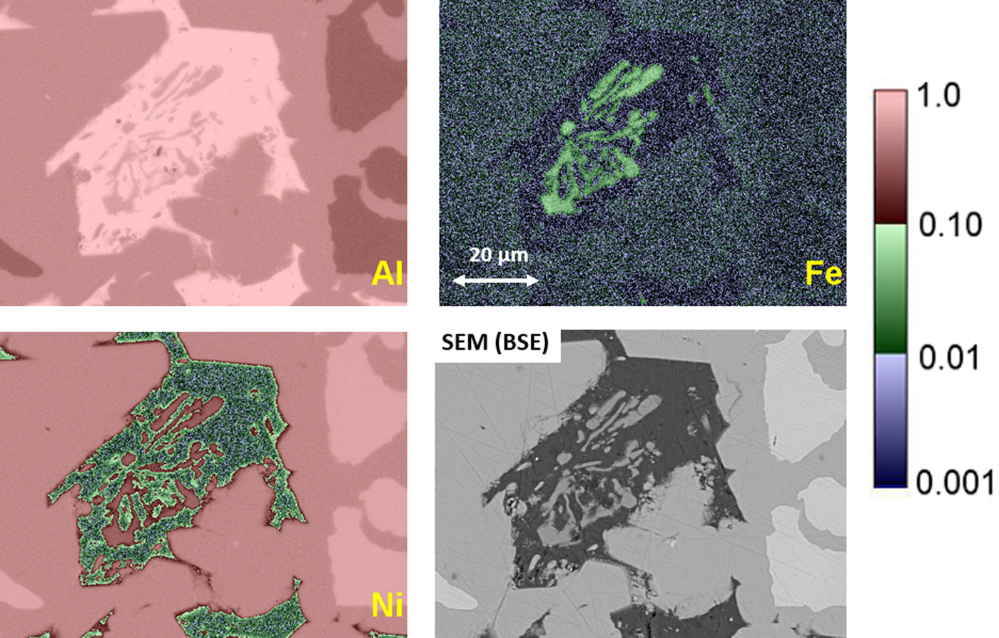
Fig. 21. Raney nickel alloy XSI with standards-based quantitative processing through NIST DTSA-II and color display using the logarithmic three-band encoding of concentration (see the embedded scale); SEM-BSE image of this area.
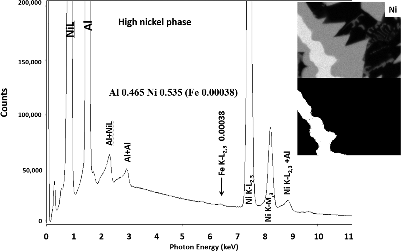
Another example of the correction of the atomic number dependence of the background is presented in Figure 22. The apparent concentration of Fe in the Al-rich and Ni-rich phases before and after quantitative corrections shows a dramatic decrease: in the Al-rich phase, the Fe concentration drops from 0.005 to 0.00015 mass fraction and in the highest Ni-containing phase, the Fe content decreases from 0.014 to 0.00038. The intermediate Ni-containing phase shows a decrease in Fe from 0.013 to 0.0027, but the level remains approximately a factor of 10 higher than the trace Fe in the Al-rich and high Ni-rich phases, creating the contrast seen. Is this contrast real? This question can be answered by selecting contiguous pixels within each phase to construct high count SUM spectra. These SUM spectra reveal low-level Fe peaks, as shown in Figure 23 (intermediate Ni-phase) and Figure 24 (high Ni-phase).
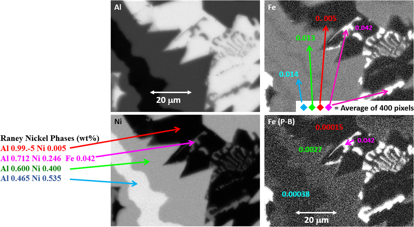
Fig. 22. Raney nickel alloy XSI showing raw intensity images for Al, Ni, and Fe, and the Fe image after quantitative processing. Note that the reduction in the false Fe contrast due to the atomic number dependence of the X-ray continuum.

Fig. 23. Derived SUM spectrum from contiguous pixels (see the inset image for selected pixel map) in the intermediate Ni-containing phase showing trace Fe.

Fig. 24. Derived SUM spectrum from contiguous pixels (see the inset image for selected pixel map) in the high Ni-containing phase showing trace Fe.
Discussion: The Next 50 Years
The examples presented in this paper demonstrate that 50 years of development of the technique of EPMA with energy dispersive spectrometry have produced a powerful elemental analysis technique. Accurate analysis (RDEV within ±5% relative in 95% of analyses) can be performed across most of the Periodic Table [currently demonstrated for Z ≥ 5 (B)] for constituents that are present as major and minor constituents. Useful accuracy (RDEV within ±50% relative) for trace constituents extends down to concentrations as low as 0.001 mass fraction (1,000 ppm) even when severe peak interference occurs from the much higher intensity peak(s) of a major or minor constituent. In the absence of peak interference, trace constituents can be measured to the limit of detection to 0.00025 mass fraction (250 ppm) or even lower. Most importantly, by inspection of the peak fitting residual spectrum, the lower intensity peaks produced by unanticipated constituents present at a much lower concentration that are hidden under higher intensity peaks can be discovered. As demonstrated in the examples presented above (Ba–Ti measured with both WDS and EDS; EDS of SRM 168), an iterative qualitative–quantitative analysis strategy can solve complicated compositions with severe peak overlap. For the analysis of major, minor, and a substantial range of trace constituents, EDS analytical performance can match that of WDS and at a much lower dose.
What are the remaining challenges to EDS analysis? Future improvements can be anticipated in the following areas:
1. The end of “black box” analytical software: The problem facing users of electron-excited EDS X-ray microanalysis is that vendors supply “black box” analytical software with no links to formally reviewed publications that describe in detail what is being done to convert the measured EDS spectrum to quantitative concentration values by means of standardless analysis. In fact, journal references alone are not sufficient. The only access to the source code can reveal the many subtle design decisions that are required to take the ideas in the journal articles and make a practical implementation. Moreover, the software is provided with no demonstration of the analytical accuracy of the particular implementation of standardless analysis through detailed studies of reference materials or other materials of known composition and homogeneity.
This situation needs to be addressed by the vendors before the users of the EDS microanalysis tool are shut out of access to publishing their scientific results in flagship journals. There are increasing demands for transparency in data access (i.e., the recorded EDS spectra and XSI with their metadata) as well as the availability of fully public software necessary to process the spectra to obtain the final concentrations along with a rigorous uncertainty budget.
2. Blunder-proof qualitative analysis: While some vendor software is better than others, we continue to routinely observe qualitative analysis blunders involving trace, minor, and occasionally major constituents. Legacy software from the era of small computers and limited memory depended by necessity upon representing an X-ray peak by a single peak channel. This single channel energy was used to select the appropriate element from a characteristic X-ray database. Because of the convolution of multiple peaks within a family, the peak channel often does not correspond to the energy of the principal member of an L- or M-family, which can result in misidentification even of major constituents (Newbury, Reference Newbury2005). The problem is exacerbated for minor and trace constituents and for operation at low beam energy (Newbury, Reference Newbury2007, Reference Newbury2009). Peak identification that is based upon fitting the full range of channels that span the entire envelope of an X-ray family provides much more robust results and has been implemented in some systems. This critical first step of properly identifying the elements present must be made invulnerable to blunders, which obviously render any subsequent quantification meaningless.
3. X-ray coincidence artifacts: EDS detection occurs one photon at a time and a digital coincidence rejection function operates to detect and discard events where two photons enter the detector closely spaced in time and are added together producing an artifact. There is a limit to the time resolution of any coincidence rejection function, so that at a sufficiently high ICR, photon coincidence artifacts occur in the recorded spectrum. Coincidence can occur for any two photon energies, such as a characteristic X-ray and a continuum X-ray, but significant and obvious artifacts are the result of the coincidence of two characteristic X-rays that result in a distinct sum peak. At high counting deadtime for a composition with several major constituents, the various combinations of parent peaks can produce a forest of artifact coincidence peaks that occupy much of the useful photon energy range (e.g., A + A, A + B, B + B, etc.). Depending on the parent peak energies, these artifact sum peaks may be mistaken for legitimate minor or trace constituent peaks. Because coincidence peaks can be modeled based upon the measured count rates of the high intensity parent peaks, a post-collection correction is applied in some vendor software to remove the coincidence peaks and redistribute the appropriate number of counts back to the parent peak(s). While this mathematical correction scheme is useful, it can introduce distortions into the spectrum that eventually limit the detection of legitimate low intensity peaks.
A more desirable treatment of coincidence would be the development of a hardware and/or software scheme for “loss-less counting” (Scoullar et al., Reference Scoullar, McLean and Evans2011). Effectively an extension of the existing coincidence rejection function, loss-less counting would enable spectra to be recorded at much higher deadtime, 50% or more. Such an improvement would make much more effective use of the high-throughput capability of SDD-EDS. While it will never be possible to distinguish two X-rays that reach the anode simultaneously, the current standard detection scheme rejects X-rays even when they can be distinguished as independent X-ray events. If two events reach the anode in less than the pulse-pair rejection time, then the resulting pulse will be indistinguishable in shape from a single pulse. In a modern pulse processor, the pre-amplified output of the SDD is immediately digitized. All the functions of the pulse processor are then implemented as a series of parallel (functioning simultaneously) digital filters on the digitized data. Typically, one data processing filter handles pulse-pair rejection in a manner similar to a fast discriminator. The data stream looks like a series of steps with nonvertical risers of varying heights and varying duration treads. The angle of the riser is a property of the SDD chip, preamplifier and the ballistic deficit, and it varies event-to-event. The duration of the treads depends upon the time separation of the events. Modern pulse processors require a certain separation of events to permit the accurate measurement of the height of the riser (the X-ray energy). However, it may be possible to characterize the tread shape as a function of the first and second riser heights and estimate the tread height with reduced accuracy but much increased speed. The two-event height (sum of the X-ray energies) would be measured accurately, but the means to apportion the energy between the two pulses would be measured less accurately. Successful implementation would require a library of many exemplars of the shape of the clean pulses, but with such a library it might be possible to train neural networks to deconvolve pulse trains with much reduced dead-time resulting in much higher throughput.
4. Improved accuracy in standardless analysis: Standards-based quantitative EDS analysis has been demonstrated to match WDS analysis for accuracy, as measured by the distribution of RDEVs, even when severe peak interference occurs. However, it must be acknowledged that the majority of quantitative EDS results that are reported in the literature are based on the application of standardless analysis despite its factor of five poorer accuracies, as indicated by the broader RDEV distribution. This situation is not surprising given the much simpler measurement requirements of the standardless method, which only requires knowledge of the beam energy and X-ray emergence angle with no need for dose information or even control of the dose. Improving the measurement science of standardless analysis should provide broad benefits to the EDS analysis community. A path forward would be the development of a detailed database of X-ray spectra of elements and stoichiometric compounds as well as microanalysis-qualified Reference Materials measured on a well-characterized EDS detector. These spectra must span the Periodic Table from Li to Pu, with some obvious exceptions, e.g., Tc, Pm, Po, At, Fr, Ra, Ac, and Pa, as well as the inert gases. A wide range of beam energies should be represented, spaced every 2.5 keV from E 0 = 30 keV to E 0 = 10 keV, every keV from E 0 = 10 keV to E 0 = 5 keV, and every 0.5 keV from 5 keV down to E 0 = 0.5 keV. These measurements should be made at several values of the X-ray detector take-off angle, e.g., 5° increments from 30 to 60°, and also at several target tilt angles, e.g., 5° increments from 0 tilt (normal beam incidence) to 60° tilt. A detailed measurement protocol must be developed to transform the library spectrum to match the performance of the local EDS efficiency on a channel-by-channel basis.
5. Alternative methods of getting dose information: The use of a Faraday cup to measure the beam current to determine dose is a critical part of the standards-based analytical protocol. Implementing such a beam current measurement can prove difficult in a scanning electron microscope platform unless the specimen stage is electrically isolated to accommodate a Faraday cup. At least one EDS vendor uses a spectrum collected from a known material as a substitute for direct measurement of probe current. The measured integrated intensity in the spectrum will scale linearly with dose, assuming all else remains constant. There are advantages and disadvantages to this procedure. The primary advantage is that the scheme calibrates for both dose and solid angle in a single measurement. This makes it easier to compensate for differences like detector area and detector-to-sample distance between the reference detector on which the stored library spectrum was collected and the user's detector. A disadvantage occurs if the detector take-off angle (X-ray emergence angle) differs between the reference detector and the user's detector, requiring that a correction factor be calculated, which has an increasing influence at lower photon energies. Another disadvantage is the longer time required to collect similar signal-to-noise dose data. The high throughput of SDD-EDS enables adequate spectral counts to be accumulated in a few seconds, with the added advantage that the integrated count can be read with greater precision than is typically available with a digital current meter.
6. Using the entire EDS spectrum: Peak-to-background (P/B) methods based upon exploiting properties of the continuum (bremsstrahlung) X-ray background become much more viable with the high-integrated count spectra made possible by the high throughput of the SDD-EDS. The use of peak-to-background methods should be viewed as complementary to the classic k-ratio methods. Peak-to-background methods do not require themeasurement of probe dose to produce a useful analytical total and peak-to-background methods are much less susceptible to sample topography, providing that the measured continuum is from the analyzed volume and is not degraded by remote sources, e.g., backscattered electrons striking other portions of the specimen or the instrument chamber. It is possible to create peak-to-background databases that are independent of the detector. Peak-to-background methods are much less sensitive to electron and X-ray transport physics and to uncertainties in mass absorption coefficients. Computers are fast enough today to permit quantifying spectra using both k-ratio methods and peak-to-background methods for all analyses. The results could be compared, and when the peak-to-background method differs substantially from the k-ratio method, the validity of the k-ratio method could be questioned. It is not a perfect scheme for identifying problems with the k-ratio analysis but it is complementary to the analytical total. Another effective use of the entire spectrum data set is to compare it to a model-based estimate of the continuum plus characteristic intensity (Statham et al., Reference Statham, Penman and Duncumb2016).
7. Spending more time designing measurements both upfront and in an iterative mode: The most advantageous route to improving the SEM/EDS community's ability to produce good compositional measurements might be measurement planning. Modern computer-controlled measurements seem too easy, but as the experienced quantitative microanalyst knows there are many pitfalls—many of which do not become evident until well into the measurement process. Software that guides users through the process of designing a measurement protocol that meets their realistic measurement needs could avoid a lot of problems. Often all that the analyst requires is a correct qualitative analysis, and the software could then guide them through the moderate challenges associated with collecting and processing a spectrum for useful quantitative information. Sometimes, a rough measurement of composition is all that is necessary. The software could use an interview that combines easily answered questions and image processing of the target area to determine the optimum beam energy and X-ray family selection strategy, as well as the best beam location(s) when the specimen topography deviates from the ideal flat polished surface. Multiple EDS detectors mounted at different azimuthal angles can be used to measure the effect of topography on the spectrum. Differences in backscatter signals from the quadrants in a multielement backscatter detector can provide crude topography information. The software should warn about, but not preclude, measurements which are suboptimal. Perhaps, a standardless analysis with realistic uncertainty bars might be sufficient. Occasionally, the analyst really wants to push the capabilities of quantitative X-ray microanalysis. Almost all good measurements are iterative. The software should support the iterative refinement of the measurement protocol based upon the analyst's measurement goals (e.g., overall uncertainty in the analysis, limit of detection, and spatial resolution). As the nature of the problem becomes better understood, the optimal measurement protocol can be refined. The first measurement might use a peak-to-background standardless analysis algorithm to seed the algorithm which selects the first-pass set of optimized standards and measurement conditions. The process should iterate until the analyst's measurement goals are met explicitly, patience is exceeded, or it becomes clear that no better measurement can be made. A large component of such a system is a complete model of measurement uncertainties which includes a comprehensive set of measurement parameters. This would enable the system to make analytical decisions based on robust models that allow it to optimize beam energy, standard selection, characteristic peak selection, analysis duration (dose), and other measurement parameters. The sources of input uncertainties would include experimental setup parameters like probe current, beam energy, sample preparation, and standard selection, and also physical parameters like mass absorption coefficient, especially when more than one X-ray family is available for an element of interest. The more aspects of the measurement model that can be included in the uncertainty calculations, the better the optimization process. We expect that in the coming decades, EDS software will become more like an experienced analyst looking over the analyst's shoulder nudging the analyst toward better measurement protocols.
8. Low beam energy analysis: Low beam energy (E 0 ≤ 5 keV) X-ray microanalysis has been made practical by the outstanding electron beam performance, e.g., size, current, and stability, of SEMs in this energy range complemented by the excellent low-photon energy performance of SDD-EDS, which can now measure photons down to energies of 40 eV or less. However, quantitative low beam energy X-ray microanalysis is much more challenging compared with analysis in the conventional beam energy range (10 keV ≤ E 0 ≤ 25 keV). Part of this challenge arises from the nature of the materials being analyzed. Most materials have a shallow surface region of environmentally modified composition due to natural oxidation, contamination, etc. Such surface layers form only a small percentage of the electron range under the conventional beam energy operation and do not significantly affect quantitative measurements. However, in the low beam energy regime, these shallow surface layers comprise a more significant fraction of the range and have a significant impact on quantitative analysis. Removal of the surface layer(s) may be possible by ion beam milling in a dual-beam platform, but under the residual partial pressure of oxygen in a conventional vacuum chamber, surface oxide layers will quickly redeposit. For inhomogeneous materials, ion beam milling can reveal unexpected subsurface structures that may not be obvious from surface SEM imaging and that may interfere with quantitative analysis performed on the original surface. While current models for quantification have been shown to be useful for solving some problems, improving the accuracy of low beam energy X-ray microanalysis, whether standards-based or standardless, will require modeling all targets as multilayered structures. Measurements at several incident beam energies will likely to be needed to assess the thickness and composition of the surface layer(s) present, supported by φ(ρ-z) and/or Monte Carlo electron trajectory modeling. Improved knowledge of the fundamental physical parameters for low energy X-ray peaks is vital for further progress. Databases of known special cases, like L-line analyses of Fe- and Ni-silicides (Gopon et al., Reference Gopon, Fournelle, Sobol and Llovet2013; Llovet et al., Reference Llovet, Pinard, Heikinheimo, Louhenkilpi and Richter2016), will help with samples for which the standard matrix correction algorithms fail.
9. Comprehensive compositional mapping: The continued development of advanced hyperspectral tools and comprehensive sensing reconstruction to efficiently mine large X-ray spectrum images in an unbiassed manner is a critical area. Metrics to optimize the characterization of heterogeneous microstructures are needed, especially for deconvolution of beam spreading effects that can compromise the interpretation of true compositional gradients at interfaces that may be of particular interest in understanding material properties and processes. The use of EDS detector arrays that surround the specimen may allow more accurate correction of the geometric effects that compromise the compositional mapping analysis of rough topographic objects. Such a capability would be invaluable in dealing with samples that must be preserved and analyzed in the as-received condition and which cannot be compromised by grinding and polishing to produce an ideal flat surface.
Acknowledgments
The authors wish to thank many colleagues throughout the microanalysis community for their interest, advice, and support through the years, especially the contributions of the late Charles (Chuck) Fiori, the architect of the original Desktop Spectrum Analyzer (DTSA) EDS analysis and modeling software.