


Introduction
Fluctuation electron microscopy (FEM) is a method to study the structure of amorphous materials and can give insight into their structural heterogeneity (Treacy et al., Reference Treacy, Gibson, Fan, Paterson and McNulty2005; Deng et al., Reference Deng, Du and Sui2012; Hwang et al., Reference Hwang, Melgarejo, Kalay, Kalay, Kramer, Stone and Voyles2012). FEM is nowadays mainly performed as a scanning transmission electron microscopy (STEM) technique: A nanometer-sized electron beam scans over the sample and acquires diffraction patterns at each position (Voyles & Muller, Reference Voyles and Muller2002). Speckle arises in these diffraction patterns due to local, coherently diffracting regions within the material. These regions can be seen as an origin of the structural heterogeneity in a disordered material and are mainly interpreted to be a form of medium-range order (MRO) (Treacy & Gibson, Reference Treacy and Gibson1996; Treacy et al., Reference Treacy, Gibson, Fan, Paterson and McNulty2005). One such form of MRO are, for instance, paracrystals in amorphous silicon which are embedded into a matrix consisting of a continuous random network (Treacy et al., Reference Treacy, Gibson and Keblinski1998). Comparable theories exist for metallic glasses, they state that their MRO is a form of ordered, yet not crystalline, nanoscale clusters (Daulton et al., Reference Daulton, Bondi and Kelton2010; Hwang & Voyles, Reference Hwang and Voyles2010; Deng et al., Reference Deng, Du and Sui2012; Hwang et al., Reference Hwang, Melgarejo, Kalay, Kalay, Kramer, Stone and Voyles2012).
Due to the disorder within the material, each diffraction pattern is unique and exhibits speckle at different scattering vectors. Intensity variations between the patterns are statistically evaluated to yield the normalized variance V(k, R) (Treacy & Gibson, Reference Treacy and Gibson1996; Voyles & Muller, Reference Voyles and Muller2002; Treacy et al., Reference Treacy, Gibson, Fan, Paterson and McNulty2005) given by
 $$\eqalign{V( k = \vert \vec{k}\vert ,\; R) & = {\langle I_d( \vec{k},\; R) ^2\rangle_{n, \phi}\over \langle I_d( \vec{k},\; R) \rangle_{n, \phi}^2}-1 \cr & \quad -{g\over \langle I_d( \vec{k},\; R) \rangle_{n, \phi}}.}$$
The normalized variance is calculated from the ratio of the two averaged intensity terms over n diffraction patterns, corresponding to the “Annular mean of variance image” method mentioned in Daulton et al. (Reference Daulton, Bondi and Kelton2010). The intensities I d denote the digitized intensity as obtained from the detector while the electron counts will be referred to as I e in the following. These quantities are connected with each other via I d = g I e with the detector gain/conversion efficiency g. The subscript ϕ indicates that the results are azimuthally averaged. The parameter R marks the probe size measured at the full width at half maximum (FWHM) of the beam intensity while k is the scattering vector magnitude. The term  $-g/\langle I_d( \vec {k},\; R) \rangle _{n, \phi }$ corrects the data for Poisson noise (shot noise) (Voyles & Muller, Reference Voyles and Muller2002; Treacy et al., Reference Treacy, Gibson, Fan, Paterson and McNulty2005; Fan et al., Reference Fan, Paterson, McNUlty, Treacy and Gibson2007) which is inherent to any electron microscopy experiment. Poisson noise affects the normalized variance considerably if a too low number of electrons I e = I d/g are detected. Normalized variance data are often acquired at several probe sizes R, this method is usually termed variable resolution FEM (VRFEM) (Voyles et al., Reference Voyles, Gibson and Treacy2000). It is possible to estimate the MRO size of an amorphous structure from VRFEM data since the variance peak magnitude depends on the probe size (Gibson et al., Reference Gibson, Treacy and Voyles2000; Hwang & Voyles, Reference Hwang and Voyles2010). The peaks are maximized when the probe size matches the MRO size (Gibson & Treacy, Reference Gibson and Treacy1997).
Apart from the probe size, there exist further parameters that influence the normalized variance. For example, sample-related aspects like the MRO volume fraction or its degree of order (Yi & Voyles, Reference Yi and Voyles2012). Additionally, the sample thickness or the fabrication process affect the data but also instrument-related factors such as the beam energy or its coherence (Li et al., Reference Li, Gu and Hufnagel2003; Yi et al., Reference Yi, Tiemeijer and Voyles2010; Yi & Voyles, Reference Yi and Voyles2011; Li et al., Reference Li, Bogle and Abelson2014). Beam coherence plays an important role for FEM (Yi et al., Reference Yi, Tiemeijer and Voyles2010) and we have expanded on this topic in previous work (Radić et al., Reference Radić, Hilke, Peterlechner, Posselt, Wilde and Bracht2020). In short, it is necessary to have a highly coherent beam for FEM experiments. This can be realized by using a very low beam current as well as a very small probe forming aperture and minimizing aberrations.
FEM simulations performed under idealized conditions show that the normalized variance should feature a baseline level of 1 with peaks protruding above it (Treacy & Gibson, Reference Treacy and Gibson2012; Rezikyan et al., Reference Rezikyan, Jibben, Rock, Zhao, Koeck, Nemanich and Treacy2015). Experimentally, such a large variance is never achieved. Rezikyan et al. (Reference Rezikyan, Jibben, Rock, Zhao, Koeck, Nemanich and Treacy2015) analyzed the experimental variance suppression with simulations and presented some experimental data as well. They concluded that displacement decoherence caused by beam–sample interactions reduces the experimental normalized variance. Furthermore, they suggested that the variance suppression can be limited by a reduction of the beam energy and the electron dose to the sample.
Compared with the work by Rezikyan et al. (Reference Rezikyan, Jibben, Rock, Zhao, Koeck, Nemanich and Treacy2015), we show further experimental data and conclude that knock-on displacements are the main mechanism for the variance suppression. The displacements induce transitions from one nearly static structural configuration to another one. These structural alterations build up with increasing electron dose. As a consequence, the diffraction pattern will not stem from a single structure but corresponds to the integrated diffracted intensity over many different structural configurations. This dampens V(k, R) as the intensity variations from one pattern to another are reduced since each pattern is associated with several structural configurations instead of a single one. This idea was also suggested by Rezikyan et al. (Reference Rezikyan, Jibben, Rock, Zhao, Koeck, Nemanich and Treacy2015). Decreasing the acceleration voltage can limit these atomic displacements since the maximum energy transfer of a beam electron to an atom is reduced. An alternative possibility to limit knock-on displacements is to reduce the electron dose to the sample, as mentioned by Rezikyan et al. (Reference Rezikyan, Jibben, Rock, Zhao, Koeck, Nemanich and Treacy2015). A low electron dose can lead to noisy diffraction patterns but this aspect can be countered by using a high binning on the detector which is explored in the present paper.
Materials and Methods
A layer of amorphous silicon was created by ion implanting an initially crystalline silicon-on-insulator wafer. The ion implantation was carried out with 28Si+ ions at the Helmholtz-Zentrum Dresden-Rossendorf. The wafer was tilted by 7° relative to the ion beam during the implantation and kept at liquid nitrogen temperature. A full amorphization was achieved by three different ion energies, namely 50, 150, 300 keV. The corresponding ion fluences were 2.2 × 10¹⁴, 2.8 × 10¹⁴, and 1.0 × 1015 cm−2. The wafer has been ex situ annealed for 12 h at 520°C after the implantation as part of previous experiments (Kirschbaum et al., Reference Kirschbaum, Teuber, Donner, Radek, Bougeard, Böttger, Hansen, Larsen, Posselt and Bracht2018).
A cross-sectional TEM lamella was fabricated out of this material with a ZEISS CrossBeam 340 focused ion beam machine. The lamella was thinned down to electron transparency with gallium ions at consecutively decreasing ion energies. The final thinning step was performed with 1 keV ions to minimize ion beam induced damage to the structure.
The experiments were conducted on a ThermoFischer Scientific (FEI) Titan Themis G3 60-300 microscope. FEM measurements were performed at a high tension of 300 and 60 kV. As mentioned, the normalized variance V(k, R) is obtained from a set of STEM diffraction patterns. The corresponding STEM probes were realized by using a mini-condensor lens in the so-called microprobe mode. They were formed by a 10 μm C2 aperture at spot size 8 and the total beam current, as determined by the fluorescent screen, was always set to I = (10 ± 1) pA. The beam current measurement with the fluorescent screen is imprecise but there was no other option available at the time of writing. The real beam currents can deviate from the nominally reported value and can moreover differ between the 300 and 60 kV experiments. Therefore, the electron doses given in the next sections are potentially subject to relatively large uncertainties. But, we want to emphasize at this point that the electron dose to the sample is not the only characteristic that determines an FEM measurement since the beam coherence depends on the probe current. For example, the normalized variance of a measurement acquired with 100 pA and a 1 s exposure can differ from an experiment conducted with 10 pA and a 10 s exposure, despite both featuring an identical dose. The relevant electron dose to the sample was calculated as 0.5 Iτ/π(R/2)2, where τ is the exposure time. The factor 0.5 appears because we are concerned with the current which passes through the area π(R/2)2 and not across the area illuminated by the entire beam. This is appropriate because the probe size R (the beam's FWHM), not the entire beam extent, marks a characteristic experimental length scale used for MRO analysis. The gun lens was set to 671 at 300 kV and to 707 at 60 kV in our experiments. The beam's semi-convergence angle α was adjusted to yield a FWHM of R = (1.50 ± 0.10) nm at both acceleration voltages. The angle α equals α 300 = 0.60 mrad at 300 kV and α 60 = 1.02 mrad at 60 kV. The STEM high-angle annular dark-field (HAADF) image seen in Figure 1 shows the sample's layered structure. Diffraction patterns were acquired from the indicated red line scan over the amorphous silicon layer. Each FEM measurement consists of 150 diffraction patterns. These were recorded on a Gatan UltraScan 1000XP CCD and a FEI Ceta 16M CMOS (speed upgrade) camera at various exposure times and two different binnings, namely binning 2 and binning 8. When binning is utilized a certain number of pixels on a detector is combined to one larger superpixel. Both cameras, the CCD and the CMOS based Ceta, have in common that primary beam electrons are converted to photons which are afterwards detected by the respective sensors. There exist several differences between these cameras, one of them being the gain/conversion efficiency g. According to their respective data sheets at the time of installation, the CCD camera has a gain of g CCD,300 = 2.45 for 300 keV electrons while the Ceta has g Ceta,300 = 6.5. The gain is not a fixed quantity, it depends on the primary electron's energy and increases for less energetic electrons (Mitchell & Nancarrow, Reference Mitchell and Nancarrow2015). We roughly estimate that the gain increases by a factor of 2.2 for 60 keV electrons on both cameras. Thus, we obtain g CCD,60 ≈ 5.39 and g Ceta,60 ≈ 14.3 at 60 kV. A precise knowledge of g for each camera and beam energy would be beneficial since it influences the Poisson noise correction for V(k, R). The correction affects the normalized variance the most when the incident electron dose and by this the counts are low. But this aspect does not compromise the interpretations extracted from our data since the main takeaways between the measurements remain valid even with imprecise g values.

Fig. 1. A STEM HAADF overview of the cross-sectionally prepared sample. The individual layers are labeled and the measurement area, a line scan, is indicated in red. The green box marks the area where the sample thickness was determined. The contrast was digitally adjusted such that all layers are clearly visible.
Another difference between the two cameras is their binning technique. The intensities of individual pixels are firstly summed up and then read out as a single superpixel on the CCD camera. In contrast, the CMOS camera firstly reads out the intensities of the individual pixels and then electronically sums those signals up to a superpixel. These different approaches influence the signal-to-noise ratio (SNR) of the two detectors regarding the readout noise: N-fold binning on the CCD improves the SNR by a factor of N 2 while the SNR improvement is limited to only N on a CMOS camera. Thus, readout noise could still compromise weak signals on a CMOS camera even when binning is utilized.
The camera length had to be re-adjusted for some experimental sets, they are listed in Table 1. The camera lengths were selected such that the pixels have a comparable scaling in reciprocal space. It was not possible to reach a full agreement between these pixel sizes since the camera length can only be set in discrete values. However, this small discrepancy is insignificant for the present FEM experiments. In order to capture a full diffraction pattern on the CMOS camera, the HAADF detector had to be retracted during the FEM acquisition.
Table 1. Varying Camera Lengths Were Necessary for the FEM Experiments.

They were adjusted to offer a comparable pixel size in reciprocal space for each setup. The values denote the pixel size at binning 2.
The sample thickness was determined by electron energy-loss (EEL) spectroscopy (Malis et al., Reference Malis, Cheng and Egerton1988) with a Gatan Quantum 965 ER. The thickness at the measurement area is given by (0.50 ± 0.08) t/λ 300 at 300 kV while it amounts to (1.14 ± 0.17) t/λ 60 at 60 kV. Here, λ i denotes the inelastic mean free path at the respective beam energy. The former thickness value was measured prior to the FEM experiments, while the latter value was determined after the final FEM measurement.
Results and Discussion
An exemplary diffraction pattern of amorphous silicon acquired on the CCD camera at 300 kV with an exposure time of 16 s (dose ≈ 2.8 × 10⁸ e−/nm2) at binning 2 is displayed in Figure 2. In this case, the diffraction pattern exhibits speckle distributed among two rings due to the amorphous structure and its coherently diffracting regions. The speckle changes from one sample position to another as it depends on the local structural configuration. Additionally, there is a diffuse intensity background in the pattern due to inelastically scattered electrons. The beamstop in the center blocks the direct beam in order to protect the camera.

Fig. 2. An exemplary diffraction pattern of amorphous silicon acquired at 300 kV on the CCD with binning 2 and an exposure time of 16 s (dose ≈ 2.8 × 10⁸ e−/nm2).
Comparison of 300 kV FEM Data with Similar Electron Doses
FEM experiments conducted at 300 kV with a nominally identical or comparable electron dose are displayed in Figures 3 and 4. Since the beam current and probe size were fixed to (10 ± 1) pA and R = (1.50 ± 0.10) nm in every case, the dose was controlled by the exposure time. Generally, all measurements exhibit the well-known double peak of amorphous silicon within the displayed scattering magnitude range. The first peak is centered at k = (3.23 ± 0.06) nm−1 while the second peak is located at k = (5.78 ± 0.08) nm−1. The measurements in Figure 3 feature a comparably large dose (≈ 1.7 × 10⁸ e−/nm2) while the ones in Figure 4 were acquired with a comparably low dose (≈ 1.1 × 10⁷ e−/nm2). The exposure time and by this the dose between the CCD and Ceta measurements are not perfectly identical in the two figures (≈ 1.7 × 10⁸ versus ≈ 1.9 × 10⁸ e−/nm2, ≈1.1 × 10⁸ versus ≈ 1.2 × 10⁸ e−/nm2) but one can draw conclusions about the data in both cases nonetheless since the doses are very close to each other.

Fig. 3. V(k, R) of different 300 kV setups which feature a similar, comparably large electron dose. Generally, there are only minor differences between the data. This suggests that comparable normalized variance data will emerge at 300 kV if experiments feature a comparable, large electron dose (≈ 1.7 × 10⁸ e−/nm2 for the CCD data and ≈ 1.9 × 10⁸ e−/nm2 for the Ceta). The Ceta needs a larger electron dose than the CCD to yield the same V(k, R).

Fig. 4. Normalized variance data of different 300 kV setups which were acquired with a comparable, low electron dose (≈ 1.1 × 10⁷ e−/nm2 for the CCD and ≈ 1.2 × 10⁷ e−/nm2 for the Ceta). Noise plays a major role for some of these measurements. The CCD binning 2 experiment is strongly influenced by Poisson noise while the Ceta binning 8 data is possibly affected by readout noise at larger scattering magnitudes. The binning 8 data of both cameras is able to resolve the two normalized variance peaks of a-Si while the CCD binning 2 data fails to do so.
The FEM theory does not take the signal processing of the data fully into account. While the influence of some noise sources and artifacts has been analyzed, such as Poisson noise, sample thickness variations, or carbon contamination (Voyles & Muller, Reference Voyles and Muller2002; Li et al., Reference Li, Bogle and Abelson2014), the effect of the detector and its parameters has not been studied in detail. One might expect that measuring the same sample position under the same conditions should yield a similar V(k, R).
For a relatively large dose as in Figure 3, only minor differences between the curves appear at 300 kV. The normalized variance of the binning 8 CCD experiment is slightly lower at the two peaks than its binning 2 counterpart. This difference can be attributed to various experimental effects. For instance, the small deviation could be caused by a minor beam current variation, which is equivalent to varying doses, between the two measurements. The Ceta measurement would have an increased normalized variance compared with the CCD data if it had an identical exposure time as the CCD measurements in this particular 300 keV setup. That is due to beam damage as will be discussed later. This disparity in V(k, R) can be attributed to different detector characteristics between the cameras. It seems that the Ceta requires more electron counts I e than the CCD in order to yield the same normalized variance.
Contrary, V(k, R) varies significantly when the experiments have a comparable low electron dose as depicted in Figure 4. This shows that the normalized variance is affected by the detector settings. Otherwise, one would expect similar V(k, R) for the three data sets as well. The normalized variance of the two CCD experiments are in agreement with each other up to k ≈ 3.3 nm−1. The binning 2 data is strongly influenced by noise for larger scattering magnitudes and the second V(k, R) peak cannot be resolved anymore. However, the binning 8 data appears much less affected by noise and is able to offer seemingly good normalized variance data up to at least k ≈ 6.5 nm−1. The binning 8 CCD normalized variance is about twice as large compared with the large dose data in Figure 3 while exhibiting identical characteristics. The Ceta data, binning 8 at 300 kV in this case, would once again be larger at all scattering magnitudes if the dose matched the dose of the CCD measurements. This emphasizes once more that the Ceta requires more electron counts to generate comparable FEM data. Nevertheless, the Ceta can resolve both normalized variance peaks, equivalent to its CCD binning 8 counterpart. Thus, it is very likely that this result can be attributed to the high binning which is common to both experiments in this case. V(k, R) strongly rises for this particular Ceta measurement at scattering magnitudes greater than k ≈ 7.0 nm−1. This Ceta measurement features about 437 digitized counts I d at k = 8.0 nm−1 within a superpixel. This superpixel is the sum of 64 individual pixels due the binning process and consequently, each of these pixels had about 6.8 digitized counts. At this low number of counts within these individual pixels, readout noise could influence the data. This applies especially to the Ceta because of its binning procedure, which is to firstly read out the individual pixels and then sum them up. As a result, we conclude that the rise of V(k, R) at larger scattering magnitudes of the Ceta data in Figure 4 could be attributed to readout noise. Lastly, these measurements show that the Poisson noise correction term alone is not sufficient to remove the effects of noise from the normalized variance.
FEM Results of Measurements with Comparable Electron Doses at 60 kV
Figure 5 displays FEM data acquired at 60 kV with a comparable electron dose of ≈ 3.5 × 10⁷ e−/nm2. In this case, the exposure times (= doses) of the three measurements are identical. The two CCD data sets practically overlap at the displayed scattering magnitudes and both maxima are well resolved. In comparison, the Ceta normalized variance is larger at both peaks while it nearly overlaps with the other two measurements at the remaining k values. Neither data set shows an increasing normalized variance toward larger scattering magnitudes, indicating that noise likely does not affect the data. An identical behavior is observed for binning 2 data of both cameras at a larger dose of ≈ 5.7 × 10⁷ e−/nm2 (not displayed). This indicates again that the camera can influence FEM data but so far we cannot give a satisfactory explanation why the Ceta yields larger V(k, R) in this experimental setup. Probably, it is not related to Poisson or readout noise nor imprecision regarding g since the counts seem sufficient for each measurement such that these parameters should not be responsible for the difference in V(k, R).

Fig. 5. 60 kV normalized variance data acquired with an identical dose (≈ 3.5 × 10⁷ e−/nm2) for different experimental configurations. The CCD curves overlap for most scattering magnitudes while the Ceta camera yields a larger normalized variance at the peaks. All measurements are able to generate reasonable FEM data.
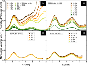
Dose Dependence of the Normalized Variance at 300 and 60 kV
Important normalized variance results are compared in Figure 6. This data shows the dependence of V(k, R) onto the exposure time/electron dose at binning 2 and binning 8 for an acceleration voltage of 300 and 60 kV. The minimum and maximum dose of each series are mentioned in the figure caption. The doses between the individual measurements differ but we can still extract and interpret trends from each data set and bring them into context with each other. The displayed data was recorded on the CCD camera, the respective Ceta data exhibit a similar behavior. This indicates that the following observations are not a detector artifact but a structural property.

Fig. 6. The dependence of V(k, R) onto the exposure time for CCD measurements. At 300 kV (a,b), the variance is continuously decreasing for increasing exposure times, equaling an increasing dose. Contrary, this decrease in V(k, R) is much less pronounced for the 60 kV experiments (c,d). These trends can be explained by beam-induced atomic displacements. The doses approximately range from 1.1 × 10⁷ to 4.2 × 10⁸ e−/nm2 in (a), from 1.1 × 10⁷ to 1.7 × 10⁸ e−/nm2 in (b), from 3.5 × 10⁷ to 1.4 × 10⁸ e−/nm2 in (c), and from 0.2 × 10⁷ to 3.5 × 10⁷ e−/nm2 in (d).
The 300 kV binning 8 data resolves the two characteristic V(k, R) peaks, even for the shortest exposure time, and offers acceptable data with relatively large peak magnitudes. The binning 2 measurements, however, require a certain threshold electron dose until a sufficient SNR level is achieved and both peaks appear.
The most important observation is that the normalized variance is continuously decreasing at 300 kV with increasing exposure times (equivalent to an increasing dose) for both binnings (Figs. 6a, 6b). This decrease affects the entire V(k, R) curves, the peaks as well as the variance at larger scattering magnitudes are being suppressed. Contrary, this effect is much less prominent in the 60 kV data (Figs. 6c, 6d). For the 60 kV binning 2 measurements, the normalized variance is very robust and exhibits only small changes as the dose is increased. The data converged toward a stable curve. A comparable statement can be made for the 60 kV binning 8 data: V(k, R) is slightly decreasing with increasing electron dose but this is primarily limited to the larger k values and indicates that the SNR of some data (0.125, 0.2, and 0.313 s exposure) is not acceptable yet. Still, the first peak and to a lesser degree the second peak remain relatively stable when the exposure time is, for instance, increased from 0.2 to 2.0 s.
The 300 kV variance trends with increasing dose are consistent with the results reported in Rezikyan et al. (Reference Rezikyan, Jibben, Rock, Zhao, Koeck, Nemanich and Treacy2015). However, the V(k, R) behavior with respect to the increasing dose at 60 kV (convergence toward a stable curve) is new.
The Impact of the Detector for FEM
Comparing the two cameras, the Ceta always yields a somewhat larger normalized variance than the CCD for FEM measurements with a comparable electron dose at both high tensions. This is partly attributed to a different binning technique which makes the Ceta more prone to readout noise in the case of low counts at low doses. However, the Ceta camera offers seemingly better FEM data than the CCD at 60 kV (Fig. 5). In that case, both V(k, R) peaks are increased compared with the CCD while the baseline level is comparable.
Generally, diffraction patterns are crucial for FEM and form the foundation to calculate the normalized variance. When the electron dose is kept identical between individual measurements, then, qualitatively, the same diffraction pattern reaches a detector but the output can vary. The camera fulfills a signal processing role: In the most general description, it captures an electron intensity distribution D e as an input, processes it and returns a digitized output O such that
 $$O = F( D_e) .$$
Naturally, this output depends on the input itself but also on the camera and its settings, depicted as a camera function F. Consequently, the normalized variance will be influenced by the camera function as well. Further studies are necessary to compare in detail how V(k, R) is affected by different detectors, including modern direct electron detectors. Beside analyzing how different detector types influence FEM data, it is also important to understand the role of the respective detector characteristics for V(k, R) of an individual detector type. For example, it would be interesting to know how V(k, R) depends on the modulation transfer function, the detection quantum efficiency, the noise characteristics, and other camera attributes of a certain detector type, for instance, CCDs. Clearly, the camera affects the normalized variance and was up until now an overlooked factor in FEM experiments and simulations. Incorporating a realistic detector into FEM simulations would offer benefits to understand its impact onto the data.
The Role of Binning for FEM
We think that the majority of the previous observations can be explained by the effect of binning and knock-on damage. Binning can reduce readout noise and the effectiveness in this regard depends on the binning approach. This varies between the CCD and Ceta and was briefly discussed previously.
More importantly for FEM, binning can also decrease Poisson noise. Take binning 8 as an example. At binning 8, the superpixel marks the sum of 64 individual pixels. These individual pixels will be referred to as subpixels from now on. In our measurements, the superpixel at binning 8 is the largest for the 300 kV Ceta experiment with a size of k = 0.0716 nm−1 in reciprocal space. Therefore, we can assume that the individual electron counts of the 64 subpixels will follow Poisson distributions with comparable mean values. That is because the subpixels are spaced apart by a small amount from each other in reciprocal space in this case. Furthermore, there are usually no too large intensity gradients within the diffraction pattern from one subpixel to another in the given setup.
Suppose the sample is illuminated by an identical electron dose between different measurements. The subpixel counts will adhere to a Poisson distribution P(C) with mean intensity  $C = C( \vec {k})$. Following the previous argumentation, one obtains a superpixel intensity close to $4gC( \vec {k})$ at binning 2 and $64gC( \vec {k})$ at binning 8. The resulting SNR regarding Poisson noise for the superpixels (neglecting other noise sources) is given by $\sqrt {4gC( \vec {k}) } = 2\sqrt {gC( \vec {k}) }$ at binning 2 and by $\sqrt {64gC( \vec {k}) } = 8\sqrt {gC( \vec {k}) }$ at binning 8 in a single diffraction pattern. Therefore, the binning 8 data can feature a 4 times better SNR (regarding Poisson noise) in the superpixels than the binning 2 counterpart on a given detector if the experiment is conducted with an identical electron dose. This thought can be connected back to the data of Figure 6 and explains why the low dose measurements at binning 8 offer acceptable FEM data while binning 2 fails to do so. This knowledge can also explain the observations linked to Figures 3–5. If the electron dose is comparably large like in Figures 3 and 5, then the SNR will be sufficient regardless of the binning for a certain range of scattering magnitudes and a similar normalized variance will emerge. If the dose is low (Fig. 4), then binning 2 data will struggle with Poisson noise, while binning 8 is able to extract much more information out of the measurement due to superior SNR for Poisson noise. Other noise sources could still comprise the data if the electron counts are very low.
Low dose, low binning FEM data contains structural information as well but it is overshadowed by Poisson noise. This aspect is depicted in Figure 7. It portrays FEM data acquired at an exposure time of 1.5 s (dose ≈ 2.7 × 10⁷ e−/nm2) on the CCD camera at 300 kV for binning 2 and binning 8. Additionally, the diffraction patterns of the binning 2 measurement were digitally rebinned in DigitalMicrograph by a factor of 4 such that they have the same size as the original binning 8 patterns. Pixels were simply summed up toward a new superpixel in this post-process rebinning. Hence, the rebinned data in Figure 7 has been termed “sum rebinned.” Similar to Figure 4, the binning 2 normalized variance is affected by Poisson noise, manifesting itself as a rising variance with increasing scattering magnitude. The binning 8 measurement is better once again and does not exhibit such a behavior. The most important observation in this figure is that the rebinned data is capable to replicate the original binning 8 data well. Systematic differences between the rebinned and the original binning 8 data begin to occur at k ≈ 6.7 nm−1. The data prove that the binning 2 data contains further structural information in the normalized variance but it is buried under the Poisson noise. Rebinning the data reduces Poisson noise, enhances the SNR and can help to extract further information out of the measurement. However, we advise against intentionally recording noisy diffraction patterns and rebinning them for structural analysis. Instead, FEM experiments should be conducted with a sufficient dose and number of counts in the patterns. Nonetheless, a comparison of the original data set with its digitally rebinned analogue seems useful in order to gauge the SNR of FEM data.

Fig. 7. The normalized variance of a low dose (≈ 2.7 × 10⁷ e−/nm2), low binning measurement (black data) is affected by Poisson noise. Its counterpart at binning 8 (red data) was acquired with the same electron dose but is much less affected by Poisson noise. This observation is identical to Figure 4. When the binning 2 diffraction patterns are digitally rebinned by a factor of 4 (blue data), they exhibit a similar V(k, R) as the original binning 8 data. As explained in the main text, we attribute this to the reduction of Poisson noise.
Binning is generally known to improve the SNR of low dose acquisitions. So, the previous discussion is not novel but we wish to emphasize its main takeaway: a high binning offers the chance to easily reduce the electron dose to the sample while maintaining a decent SNR. This can be vital for FEM if knock-on displacements affect an amorphous structure as the upcoming subsection will discuss. Lastly, it is important to find an acceptable combination of binning and camera length such that the speckle covers several pixels in the diffraction pattern and this was ensured for our experiments. Otherwise, suppressed intensity fluctuations are to be expected since too much information is averaged out.
Variance Suppression Due to Knock-On Displacements
The diffraction pattern is the scattered intensity integrated over the exposure time. As the exposure time increases, there are two experimental effects that can lead to a reduction of V(k, R). The first aspect is sample drift. For prolonged times, drift will influence the normalized variance because the diffraction pattern does not correspond to the scattered intensity of one fixed location but to that of several locations. As a result, the intensity variations between the patterns will decrease which, in turn, decreases the variance. While drift certainly can influence data of long exposure measurements, it cannot explain why V(k, R) seems to converge for 60 kV experiments while it persistently decreases for 300 kV ones as the exposure time is increased.
The second factor which can reduce the normalized variance are inelastic beam–sample interactions. Here, we focus on knock-on displacements. When a diffraction pattern is acquired, the beam can potentially alter the amorphous structure such that the pattern corresponds to the scattered intensity integrated over many structural configurations. Suppose that S 1 marks the structural configuration at the beginning of the exposure. Electrons get diffracted as they pass through the sample and the associated momentary diffraction pattern D 1 is being acquired by the camera. However, at a certain point in time an electron will displace an atom within the material and a new structural configuration S 2 ≠ S 1 emerges. This modification to the structure might be small but can nonetheless influence the diffraction pattern. The camera then acquires an intensity distribution associated with a momentary diffraction pattern D 2 ≠ D 1. This intensity is added on top of the previously acquired intensity linked to the momentary diffraction pattern D 1. This process will continue as long as the beam illuminates the sample. In the end, the camera outputs a diffraction pattern D that is the sum of j momentary diffraction patterns  $D = \sum _i^j D_i$. Thus, V(k, R) can be suppressed as the fluctuations between diffraction patterns taken at different measurement positions are reduced. Each individual pattern D is associated with several structural configurations S i instead of just a single one. Ideally, the camera would record a single static diffraction pattern D i throughout the entire acquisition of a pattern such that D = D i at each position.
Knock-on displacements are more likely to occur at 300 keV than at 60 keV since the maximum possible energy transfer E max = E 0(1.02 + E 0/106)/(465.7A) (Egerton et al., Reference Egerton, Li and Malac2004) of an electron to an atom is larger at higher beam energies. Here, E 0 marks the beam electron energy (in eV) and A the atomic mass number. For silicon, one obtains E max,300 ≈ 30.28 eV for 300 keV electrons and E max,60 ≈ 4.95 eV for 60 keV electrons. In comparison, the average threshold energy for the creation of a bond defect complex or a Frenkel pair, as determined by density functional theory molecular dynamics simulations, amounts to E d,c‑Si = 24 eV in most lattice directions of crystalline silicon (Holmström et al., Reference Holmström, Kuronen and Nordlund2008). Amorphous silicon features a distorted fourfold tetrahedral bonding network along with floating and dangling bonds. Consequently, the disordered material has a similar short-range order as its crystalline counterpart and we assume the same average threshold energy E d,a‑Si = 24 eV as a rough estimate. There will be a distribution of threshold energies present in amorphous silicon, similar to its crystalline phase, and locally the threshold for an atomic displacement by the electron beam can be reduced. The minimal displacement threshold energy in crystalline silicon is given by E d,c‑Si,min = 12.5 eV in the 〈111〉 direction (Holmström et al., Reference Holmström, Kuronen and Nordlund2008). It is possible that individual atoms in amorphous silicon might have an even lower threshold energy, especially if the atoms are part of a defect complex.
Next, we calculate the total displacement cross-section and estimate how many atoms are displaced by the electron beam every second within a given sample volume. The total displacement cross-section σd can be calculated by
 $$\eqalign{\sigma_d & = 0.2493 Z^2 {1-\beta^2\over \beta^4} \left[{E_{{\rm max}}\over E_d}-1 \right.\cr & -2\pi \alpha \beta + 2 \pi \alpha \beta \sqrt{{E_{{\rm max}}\over E_d}} \cr & \left. -( \beta^2 + \pi \alpha \beta ) \ln \left({E_{{\rm max}}\over E_d} \right)\right][ {\rm barn}] .}$$
This equation can be found in Seitz & Koehler (Reference Seitz and Koehler1956). It follows from expanding the Mott differential cross-section (Mott, Reference Mott1929), which describes the Coulomb scattering of a relativistic electron and a nucleus, into a power series (McKinley & Feshbach, Reference McKinley and Feshbach1948) and integrating the differential cross-section to yield the total cross-section. Here, Z denotes the atomic number, β is given by β = v/c with the relativistic beam electron velocity v and the velocity of light c and α ≈ Z/137. This total displacement cross-section is valid under the condition that E d < E max < 2E d. In the Kinchin-Pease formalism (Kinchin & Pease, Reference Kinchin and Pease1955), this equals the regime where one beam electron displaces only one atom. Additionally, the equation is only valid for  $Z \lessapprox 27$ (McKinley & Feshbach, Reference McKinley and Feshbach1948).
A total displacement cross-section of  $\sigma _{d, 300} = 6.72\times $ $10^{-28}\ {\rm m}^2 = 6.72\,{\rm b}$ is obtained for 300 keV electrons using the previously calculated values for E max and E d for silicon. At 60 kV, the displacement cross-section is negative because E max < E d and thus further calculations will not be pursued. At a beam current of 10 pA, it follows that a total of ≈ 6.24 × 10⁷ electrons pass through the sample each second. Assuming, for simplicity, that the beam profile is described by a two-dimensional Gaussian function with FWHM R = 1.50 nm in each direction, we utilize the beam current passing through the area π(R/2)2. Using R is reasonable as this length scale is usually used to obtain estimates for the MRO in an amorphous material. This area contains $50\percnt$ of the beam's total current which is equal to n e ≈ 3.12 × 10⁷ electrons passing it every second. The corresponding electron flux is then J = n e/π(R/2)2. With these values, we can estimate the displacements d per second within a given volume V for a thin sample (Cahn, Reference Cahn1959; Goland, Reference Goland1962), which is given by
 $$d = \sigma_d \rho V J,\; $$
where ρ is the material's atomic density. For amorphous silicon, we use ρ = 4.9 × 1028 atoms/m3 (Custer et al., Reference Custer, Thompson, Jacobson, Poate, Roorda, Sinke and Spaepen1994). Suppose the illuminated sample volume is a t = 100 nm long cylinder with a base area of π(R/2)2, thus V = tπ(R/2)2. Finally, we calculate the number of beam-induced atomic displacements within this cylinder and obtain d = σ d · ρ · tπ(R/2)2 · n e/π(R/2)2 = σ dρt n e = 102 displaced atoms per second. Next, we bring this number into context with the number of atoms within the illuminated sample volume, which is simply ρV = 8,659 atoms. Consequently about  $1.2\percnt$ of the atoms get displaced each second by the electron beam in the given situation. This number is a rough estimate and does not include all possible physical effects. Nonetheless, it provides valuable insight that about 1% of the silicon atoms get displaced each second by a 300 kV electron beam with FWHM R = 1.50 nm and total current of 10 pA in the given illuminated sample volume.
It is important to consider how VRFEM measurements (acquisition of FEM data with different probe sizes) are influenced by beam damage. Usually, the beam current and exposure time are fixed for VRFEM experiments such that the number of displacements d is constant for every probe size R. However, the illuminated sample volume varies since the probe size itself is being varied. Thus, it is expected that knock-on displacements will affect FEM data acquired with small R considerably more than data acquired with large R. The severity of beam damage, therefore, depends on the probe size and it has to be minimized for VRFEM experiments to ensure comparability for the data.
For long exposure times/large doses, the number of displacements can be large at 300 kV. In the above example, an exposure time of 10 s (equivalent relevant dose ≈ 1.8 × 10⁸ e−/nm2) implies that  $11.8\percnt$ of the atoms would be displaced during the acquisition within the considered volume. This is a considerable amount and a suppressed normalized variance due to structural fluctuations is to be expected.
This result emphasizes the importance of knock-on damage for 300 kV FEM measurements of a-Si and helps to explain the observations linked to Figure 6. The normalized variance is continuously decreasing with increasing exposure time/electron dose at 300 kV. Thermal vibrations of the atoms cannot be responsible for this observation since these should affect the FEM data independent of the beam energy. Instead, the electron beam persistently modifies the atomic structure during the acquisition which suppresses the normalized variance. A similar behavior is to be expected for any kind of material when the electron beam surpasses the material's displacement threshold. In the case of multi-element systems like metallic glasses, which are often studied with FEM, the component with the lowest atomic number is most susceptible to knock-on displacements because the incident electron can transfer the most energy to it. But, the maximum energy transfer has also to be set in relation to the displacement threshold energy of the material. Glasses with a large amount of free volume or that were subject to large deformations could have a low threshold energy such that displacements during FEM experiments might occur also for heavier atoms.
A dose series similar to the ones displayed in Figure 6 was acquired for as-cast Pd40Ni40P20 at 300 keV in Radić et al. (Reference Radić, Hilke, Peterlechner, Posselt, Wilde and Bracht2020). The normalized variance of this metallic glass seemed more robust than amorphous silicon toward the increasing electron dose at this beam energy. Once an appropriate SNR was reached, V(k, R) continued to only slightly decrease at the peaks for the glass. Likely, beam-induced atomic displacements mainly occur for the phosphorus atoms in the glass since its the lightest element in this composition.
It is safe to assume that beam-induced atomic displacements play a small role for 60 keV electrons passing through amorphous silicon. Thus, the diffraction pattern rather approaches a snapshot of the disordered structure at each measurement position. This suggests very few beam-induced structural alterations which should result in a better normalized variance. Increasing the exposure time then only improves the SNR further until drift begins to play a role which, as explained, will negatively impact V(k, R). This is in very good agreement with the data of Figures 6c and 6d.
An alternative way to study beam-induced structural modifications could be to position the electron beam at a fixed position and to monitor the diffraction pattern over time, similar to diffraction-based electron correlation microscopy (He et al., Reference He, Zhang, Besser, Kramer and Voyles2015). Since such a setup is susceptible to drift, it might be the best to choose a rather large electron dose and to keep the total experimental time as short as possible. We expect that the correlations between the patterns should decay faster for the 300 keV than for the 60 keV experiment.
Another key result is that a high binning provides an easy opportunity to decrease the electron dose to the sample which, in turn, decreases the number of beam-induced atomic displacements. At the same time, a high binning is capable to reduce Poisson noise as previously described. Consequently, high binning (binning 8 and larger) in combination with a relatively short exposure time/low dose can offer FEM data with an acceptable SNR and limited amount of knock-on displacements at 300 kV (or any other electron energy where knock-on displacements are a concern). During the relatively low doses of a binning 8 FEM experiment, one obtains a partial snapshot of the structure rather than an averaged structure as for large dose binning 2 FEM experiments. This is more apparent for 300 kV data than for 60 kV data. An alternative to a high binning could be to acquire the experiment at a very short camera length. In that case, the intensity of individual speckles is distributed onto a smaller detector area, leading to enhanced electron counts in the pixels. Thus, the electron dose could be decreased for such measurements too, resulting in less beam-induced structural modifications while maintaining an acceptable SNR.
A further benefit of 60 kV FEM experiments is a larger scattering cross-section. Therefore, the exposure time/incident electron dose can be selected shorter than for 300 kV measurements while still resulting in a sufficient SNR. Consequently, 60 kV FEM data can be less influenced by drift as well. But this larger scattering cross-section comes with a drawback. It results in a larger inelastic background intensity within the diffraction patterns which can suppress the normalized variance. Furthermore, enhanced multiple scattering can negatively influence the measurements as well. Here, the sample thickness amounted to t/λ 60 ≈ 1.14 at 60 kV but the FEM results still seemed to be acceptable for an analysis. Though, a thinner sample is preferred to reduce multiple scattering and inelastic effects. Generally, we think that the presented results concerning beam damage and binning are quite robust regarding the sample thickness and that the same trend should emerge for thinner or even thicker samples. The absolute value of the normalized variance data will vary however if the sample thickness were to be changed.
Additional proof for the damaging effect of high energy electrons to amorphous silicon is shown in Figure 8. This figure shows the averaged sample thickness in terms of t/λ across the amorphous silicon layer, the data were acquired at 60 kV after all FEM experiments. All FEM measurements were conducted on one and the same sample region as could be seen in Figure 1. That sample region has been thinned further by the electron beam, most likely by sputtering of surface atoms. This process could have occurred at both beam energies since surface atoms are usually weakly bound. The sample thickness decreased from t/λ 60 ≈ 1.17 to t/λ 60 ≈ 1.14 after repeated exposure. While the effect is very small, it is nonetheless present and underlines that atomic displacements and beam damage in general can affect FEM data of amorphous silicon, especially during long exposure/large dose measurements.

Fig. 8. A thickness profile across the amorphous silicon layer as determined by EEL spectra at 60 kV. The thickness was averaged over the green box from Figure 1, the zero position on the abscissa marks the interface between the Pt layer and the amorphous silicon. The sample thickness decreases at the measurement area due to repeated FEM experiments.
Comparison of Normalized Variance Data at Different Energies but Identical Dose
Figure 9 compares two normalized variance curves acquired with a nominally identical dose of ≈ 3.5 × 10⁷ e−/nm2 at 300 and 60 kV at binning 8. As mentioned previously, the beam current determination via the viewing screen is imprecise, and therefore, the electron doses are to be taken with care.

Fig. 9. Comparsion of V(k, R) at a nominally identical dose (≈ 3.5 × 10⁷ e−/nm2) at 300 and 60 kV at binning 8. In this case, the 300 kV measurement yields a larger normalized variance. This is mainly due to varying relative sample thicknesses.
Here, the 300 kV data exhibits a larger variance than its 60 kV counterpart which is in contrast to a similar comparison presented in Rezikyan et al. (Reference Rezikyan, Jibben, Rock, Zhao, Koeck, Nemanich and Treacy2015) and appears to contradict the previous discussing regarding knock-on displacements and that 60 kV data should yield a larger variance.
The sample thicknesses in terms of the inelastic mean free path of the two measurements differ which is the main reason for this unexpected result. The sample appears “thicker” for 60 kV electrons than for 300 kV electrons due to enhanced interaction cross-sections. This yields a comparatively large inelastic background intensity for the 60 kV data which suppress the normalized variance stronger. Additionally, multiple scattering occurs more frequently at 60 kV which suppresses the data even further. Here, the relative sample thickness at 60 kV is about 2.25 times larger than at 300 kV. FEM studies in the past concluded that the normalized variance roughly decays with 1/t (Yi & Voyles, Reference Yi and Voyles2011; Treacy & Gibson, Reference Treacy and Gibson2012), where t is the absolute thickness. This relationship applies to FEM data at a single beam energy. Possibly, measurements should be rescaled to a reference relative sample thickness when comparing data of different beam energies.
Furthermore, but of less importance here, the normalized variance difference between 300 and 60 kV measurements of a-Si depends on the electron dose. As portrayed in Figure 6 and explained in the subsequent discussion, the 300 kV V(k, R) data is sensitive to the electron dose and decreases continuously as the dose increases due to knock-on displacements. On the other hand, 60 kV data is less affected by beam-driven structural alterations. The comparative measurements in Rezikyan et al. (Reference Rezikyan, Jibben, Rock, Zhao, Koeck, Nemanich and Treacy2015) had a very large dose of ≈ 3.6 × 10⁹ e−/nm2, which is 100 times more than the data shown in Figure 9. Thus, their 200 kV data most likely experiences much more beam-induced displacements than their 80 kV experiment, leading to a considerably larger variance suppression at 200 kV.
Therefore, the difference of normalized variances acquired at identical doses but different beam energies depends on the discrepancy between the relative sample thicknesses in terms of t/λ at the respective beam energies. Varying degrees of the inelastic background intensity in the diffraction patterns as well as multiple scattering result in a varying variance suppression. Additionally, the variance difference can depend on the absolute value of the electron dose due to different amounts of knock-on displacements.
Energy Filtering
Additional FEM data was acquired at 60 kV by using energy filtering, these results are displayed in Figure 10. For this purpose, a 20 eV wide slit has been centered around the zero-loss of the EEL spectra. This experiment could only be conducted on the CCD, as only this camera is part of the Gatan Imaging Filter system. The two energy-filtered measurements feature an identical digitized intensity I d and were acquired at binning 2 and binning 8. These experiments can be compared with their unfiltered counterparts recorded with an identical exposure time. The mean diffracted intensity is approximately 3.2 times smaller after filtering compared with the unfiltered data for the given material, thickness, and beam energy. The energy-filtered diffraction pattern (Fig. 11) significantly differs from an unfiltered pattern. A large fraction of the inelastic, diffusely scattered background intensity between the speckle was removed and the contrast is greatly enhanced.

Fig. 10. Energy filtering at 60 kV dramatically increases the normalized variance. The energy filtered data is abbreviated by “EF” in the legend. The doses amount to approximately 8.8 × 10⁷ and 5.5 × 10⁶ e−/nm2.

Fig. 11. An energy-filtered diffraction pattern recorded at 60 kV on the CCD with binning 2 and an exposure time of 5 s (dose ≈ 8.8 × 10⁷ e−/nm2). The speckle contrast is tremendously enhanced after energy filtering compared with an unfiltered pattern as in Figure 2.
The literature predicts a small influence onto the normalized variance by energy filtering (Yi & Voyles, Reference Yi and Voyles2011). In their case, the peak normalized variance increased by ≈17% due to energy filtering the diffraction patterns. However, Figure 10 reveals a strong increase of V(k, R) because of energy filtering for our work. This increase applies to both binnings. Moreover, the variance curves exhibit some subfeatures. While energy filtering decreases the mean intensity by removing the inelastic background, the SNR of the energy filtered data is acceptable as the speckle intensity is still sufficient for an evaluation since an increase of V(k, R) for large k is absent. As a quality check, the FEM data was tested by post-process rebinning. As previously described, this procedure can help to improve the SNR of noisy data (see Fig. 7). The post-process rebinning was applied to both energy filtered data sets and it leads to a reduction of V(k, R) by 5–15%. Thus, if the exposure time would have been larger, say twice as long, the normalized variance would still be much greater after the energy filtering compared with the unfiltered data. In general, the impact of energy filtering depends sensitively on the sample thickness. If the sample were thinner, the disparity between the filtered and unfiltered normalized variance should decrease. The appearance of subfeatures in the energy filtered V(k, R) curves is interesting. Most likely this is an effect of the improved speckle contrast and reduced diffuse background intensity. Speckle between the two rings is overshadowed by the diffuse background intensity in the unfiltered diffraction patterns. Such weak, overshadowed speckle between the two rings can be identified in Figure 2 upon closer inspection.
Summary
Atomic displacements due to the electron beam negatively affect FEM measurements. Intensity variations between diffraction patterns of an amorphous material decrease due to this effect which results in a suppressed normalized variance. However, these knock-on displacements can be controlled experimentally. One option is to utilize an acceleration voltage where the maximum energy transfer of an electron to an atom is lower than the displacement threshold energy of the material. For amorphous silicon, 60 kV is a good choice in this regard. If the high tension cannot be varied, then displacements can be reduced by performing the measurement at a relatively low electron dose combined with a high binning. Care must be taken to ensure a sufficient SNR of the individual diffraction patterns. But this requirement should be easy to fulfill since high binning reduces Poisson noise considerably. The resulting FEM data will then be less compromised by knock-on displacements as the experiment features a relatively low electron dose. Ideally, all these aspects, namely a low acceleration voltage along with short exposures/low doses and a high binning, are utilized together. Short exposure times furthermore imply less drift during the acquisition of each diffraction pattern. These results agree with the interpretations and ideas of Rezikyan et al. (Reference Rezikyan, Jibben, Rock, Zhao, Koeck, Nemanich and Treacy2015). We think that beam-induced transitions from one nearly static structure to another along with a background intensity due to various inelastic scattering processes are the main mechanism behind the variance suppression when compared with idealized simulations. The latter can be minimized with energy filtering. Energy filtering can improve FEM data tremendously and should be used in any FEM setup. We recommend a high binning for energy-filtered FEM experiments as well. Lastly, the normalized variance is affected by the detector to a certain degree. In the present study, the normalized variance is larger for the Ceta CMOS camera than for the CCD in every setup. Further work is required to analyze how the camera and its parameters affect FEM data in detail.
Acknowledgments
Funding of our TEM equipment by the Deutsche Forschungsgemeinschaft (DFG) via the Major Research Instrumentation Programme under INST 211/719-1 FUGG is greatly appreciated by all authors. D.R. and H.B. are grateful for funding by DFG via BR 1520/21-1, M.P. by DFG via PE 2290/3-1 and M.P. for funding by DFG via PO 436/9-1.


 Open access