Introduction
The role of hydrogen in the passivation and activation of dopants in MOCVD grown GaN is commonly recognized, however, experimental knowledge on its behavior remains still incomplete [Reference Van de Walle and Johnson1]. Recent interest in GaN-based devices has stimulated studies on p-type doping issues [Reference Pearton and Lee2, Reference Neugebauer and Van de Walle3] as well as the search for novel ohmic contacts. In particular, Murakami [Reference Murakami and Koide4] recommended metals with high binding energies to hydrogen for making ohmic contacts to p-type GaN, and this idea has been experimentally verified with the use of Ta/Ti contacts [Reference Suzuki, Kawakami, Arai, Kobayashi, Koide, Uemura, Shibata and Murakami5]. These contacts provided the lowest reported contact resistivity values (3×10⁻⁵ Ωcm2 for hole concentration of 7×1017cm−3), but they quickly degraded.
The accumulation of hydrogen in areas of high defect density has been considered [Reference Pearton, Bendi, Jones, Krishnamoorthy, Wilson, Karlicek and Stall6], it is therefore very likely that hydrogen could be gettered in the superficial layer of p-GaN. In consequence, the subsurface volume may be characterized by a free carrier concentration lower than the bulk. The present study explores the problem of the accumulation of hydrogen in the near-surface region of p-GaN and the possibility of its removal by using ZrN/ZrB2 metallization and annealing. Zirconium possesses one of the highest absorptive capabilities for hydrogen of metal hydride systems, while ZrN and ZrB2 are distinguished for their exceptional low resistivities and high melting points. The content of hydrogen was quantified using secondary ion mass spectrometry (SIMS), while the stability of Zr-based caps on GaN under annealing has been examined using transmission electron microscopy (TEM) together with SIMS.
Experimental Procedure
The samples used in this study were (0001) oriented, Mg-doped GaN epilayers, 0.5-2 μm thick, grown via MOCVD on undoped GaN, with AlN buffer films predeposited on 6H-SiC or sapphire substrates. The hole concentration was p = 1−5*1017cm−3. Prior to insertion into the deposition chamber, the surface of GaN was etched in buffered HF, and dipped in NH4OH:H2O (1:10).
Thin films of Zr-N and Zr-B were deposited by DC magnetron sputtering in Ar discharge, from ZrN(99.5%) and ZrB2 (99.5%) targets, respectively. The process parameters were first optimized with regard to the stoichiometric composition of deposited films. Finally, a bilayer ZrN/ZrB2 metallization of a thickness (100nm)/(100nm), sequentially deposited without breaking the vacuum, was used throughout this study. Heat treatments were carried out in a rapid thermal annealer (RTA), in flowing N2, at temperatures in the range 700-1150°C for time 30 s. to 5 min. During RTA the samples were protected by a piece of GaN/Al203 as a proximity cap.
The evolution of the microstructure of Zr-based films deposited on GaN, under annealing, was investigated by cross-sectional transmission electron microscopy (XTEM) and high resolution imaging (HREM) in JEOL 2000EX microscope. SIMS profiling was performed with a Cameca 6F instrument using either oxygen or cesium primary beam.
The electrical characterization involved measuring the current-voltage characteristics and the specific contact resistance using circular transmission line method. A complementary study of electrical properties of Zr-based contacts to n-type GaN (n = 1*1017cm−3) has also been carried out.
Results
Microstructure and thermal stability of GaN/ZrN/ZrB2 system
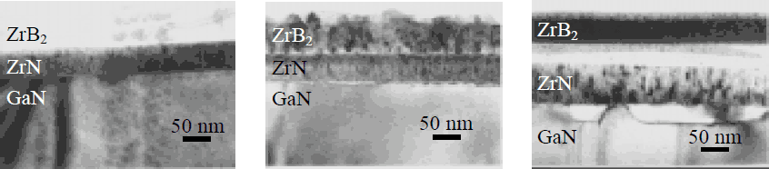
The as-deposited ZrN and ZrB2 films exhibit golden-yellow and pale-yellow color, respectively, characteristic of stoichiometric compounds. XTEM micrographs and corresponding SIMS profiles of as-deposited and annealed GaN/ZrN/ZrB2 structures are given in Fig. 1 and 2. The initial morphology of ZrN film is amorphous with islands of fine-grain polycrystalline material. ZrB2 film is amorphous. Annealing at 800°C causes partial crystallization of ZrN into elongated grains, whereas the microstructure of ZrB2 film does not change noticeably. The final morphology, after annealing at 1100°C, of ZrN film is columnar, while the ZrB2 top layer reveals a fine-grained structure. SIMS depth profiles of 11B+, 14N+, 90Zr+, 90Zr14N and 69Ga+, measured using O2 + primary beam, has been chosen to illustrate the in-depth structure of GaN/ZrN/ZrB2 contacts. In Fig. 2.a., a relatively high value of 90Zr14N signal in ZrB2 layer is a result of 90Zr14N and 94Zr10B mass interference. Similarly, the high intensity of 90Zr in GaN layer is probably due to the interference with gallium-nitrogen cluster – the 5 orders of magnitude decrease of the 90Zr14N profile in GaN near the interface region indicates that Zr does not penetrate significantly into GaN.

Figure 1. XTEM micrographs of GaN/ZrN/ZrB2 contact: a) as-deposited, b) annealed at 800°C, 5 min., c) annealed at 1100°C, 30 s.

Figure 2. SIMS profiles for GaN/ZrN/ZrB2 contact: a) as-deposited, b) annealed at 800°C, 5 min., c) annealed at 1100°C, 30 s.
SIMS depth profiles of contacts unprocessed and heat treated at 800°C indicate that GaN/ZrN/ZrB2 system remains stable. In contacts subjected to annealing at 1100°C, however, the Ga signal in Zr-containing films increases about two orders of magnitude, suggesting that the interaction at the GaN/ZrN interface has taken place.
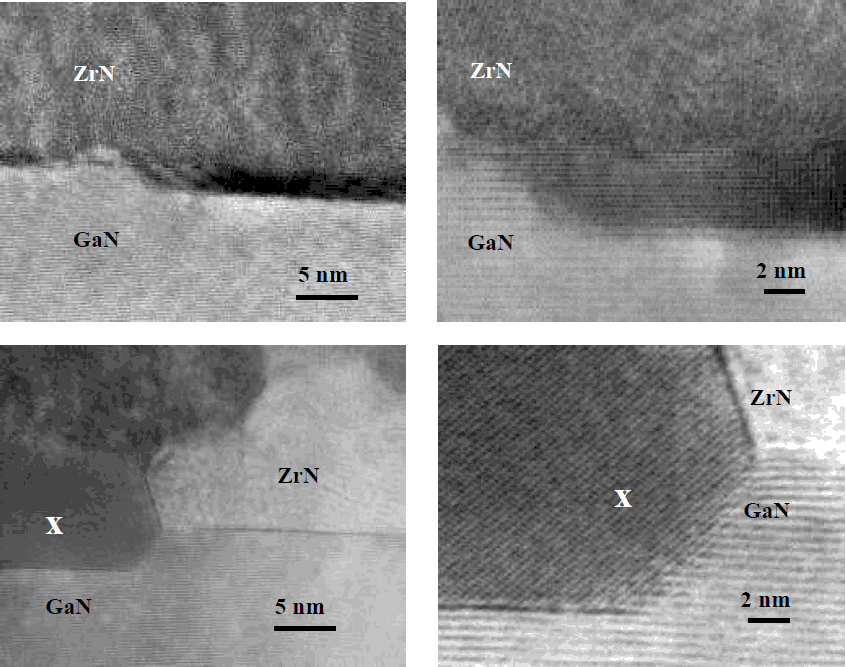
In order to evaluate the extent of this interaction, in Fig. 3 are shown HREM images of GaN/ZrN interfaces after annealing at 800°C and 1100°C. While the interface of the contact processed at 800°C is sharp and abrupt, regular intrusions form at the GaN/ZrN interface annealed at 1100°C. High-resolution image and electron diffraction pattern revealed evidence for the formation of a new phase, lattice-matched to GaN. This phase, composed of Ga, Zr and N, as indicated by EDX analysis, could not be identified as yet.

Figure 3. HREM images of GaN/ZrN interface after annealing at: a) 800°C, 5 min., b) 1100°C, 30 s.
Hydrogen in GaN/ZrN/ZrB2 system
The behavior of hydrogen in GaN/ZrN/ZrB2 under annealing was studied with SIMS. Since Zr has a high affinity for hydrogen, it is obvious that some hydrogen is trapped in Zr-based metallization during the sputter-deposition. In Table I are shown relative H- yields, with respect to Zr- ions, in ZrN and ZrB2 films as a function of annealing temperature. A noticeable evolution of hydrogen starts at 750°C from ZrB2 layer. After heat treatment at 850°C the Zr-based metallization is practically free of hydrogen.
Table I. Relative H- yields with respect to Zr- in ZrN and ZrB2 films after annealing.

Mg and hydrogen depth profiles in GaN are presented in Fig. 4. Concentrations of hydrogen and Mg in GaN were evaluated using relative sensitivity factors from ref. [Reference Erickson, Gao and Wilson7]. While the level of Mg in the entire layer of p-type GaN remains constant, a noticeably higher concentration of hydrogen in the near-surface region is clearly seen. For comparison, we have also analyzed the profile of hydrogen in n-GaN, confirming the absence of this impurity in n-type MOCVD-grown material with the detection limit ∼1017cm−3. Heat treatment at 800°C, i.e. at temperature effective for activation of Mg as a dopant [Reference Gotz, Johnson, Walker, Bour and Street8], left the amount of hydrogen in p-type material practically unchanged. The process of evolution of hydrogen from the subcontact region starts at about 900°C, and after annealing at 1100°C the level of this impurity in the subsurface layer of p-GaN is substantially reduced, as demonstrated in Fig. 4.b.

Figure 4. Magnesium and hydrogen depth profiles in p-GaN annealed under ZrN/ZrB2: a) as-deposited and annealed at 800°C, 5 min., b) as-deposited and annealed at 1100°C, 30 s.
Electrical properties of GaN/ZrN/ZrB2 contacts
The release of hydrogen from p-GaN subsurface region perfectly correlates with the electrical properties of GaN/ZrN/ZrB2 contacts. Contacts annealed below 900°C are non-linear and highly resistive. After heat treatment at 900°C for 30 sec. they become linear. The minimum specific contact resistance of 1*10−4 Ωcm−3 (p = 5*1017cm−3) was observed for contacts annealed at 1000°C. Annealing at 1100°C causes the increase of the contact resistivity. Ohmic contacts formed at 1000°C were subjected to accelerated life-time testing at 600°C for 8 hours in N2 flow. Both, the low value of specific contact resistance and the surface morphology were preserved throughout the aging.
ZrN/ZrB2 contacts, when deposited on n-type GaN become ohmic after heat treatment at 1100°C for 30 sec. with a resistivity of 6*10−4 Ωcm−3(n = 1*1017cm−3).
Discussion and Conclusions
We have shown that Zr-based metallization can effectively remove hydrogen from the p-type GaN subsurface which eventually leads to the formation of an ohmic contact. As the release of hydrogen starts at temperatures as high as 900°C, the thermal stability of the contact system is of particular importance. The thermal behavior of the ZrN/ZrB2 metallization is associated to the microstructure of each individual Zr-based compound, as well as to the interfacial crystalline accommodation. Amorphous transition metal nitrides have been previously proven as effective diffusion barriers in integrated circuits technology [Reference Krusin-Elbaum, Wittmer, Ting and Cuomo9], for thermal treatments up to 600°C. In this work we demonstrate that by properly designing the configuration of the metallization system, the thermal stability of Zr-based compounds can be enhanced well above their crystallization temperature. The use of ZrB2 layer on top of ZrN film effectively encapsulates the system, preventing the decomposition of the surface of GaN under annealing, even in case when the microstructure of ZrN film becomes columnar with grain boundaries providing the path for fast diffusion. On the other hand, ZrN interlayer between GaN and ZrB2 film impedes the recrystallization of the latter.
Whereas Zr-based metallization enables hydrogen to outdiffuse from p-type subcontact region, the resistivity of ohmic contact increases, when the thermal processing is conducted at temperature ∼1100°C, Our experiments clearly demonstrate that this coincides with a reaction at the contact interface. Thus the degradation of ohmic contact properties can be explained in terms of the decomposition of GaN and formation of nitrogen vacancies, being donors that compensate Mg acceptor centers. This would also explain the ohmic behavior, observed after heat treatment at 1100°C, when the same metallization scheme is applied to n-type GaN.
Acknowledgements
This work was partially supported by the Committee for Scientific Research, grant No. PBZ 28.11/P9.