


Introduction
With the drastic increase of users, Internet of Thing devices and Machine to Machine communications, the 4G network has been challenged motivating an evolution to 5G. The radio frequency (RF) and microwave industry has made considerable progress in enabling the development of a commercial 5G wireless infrastructure below 6 GHz. The preliminary work on 5G performed in recent years has defined a set of telecommunication standards and scalable architectures to deliver the promised data rate.
To increase the capacity for the 5G network, two paths are combined: using more bandwidth and deploying antenna arrays. RF architectures for 5G systems move towards massive multi-inputs multi-outputs (mMIMO) systems where beam forming is used to improve the spectral efficiency. By combining these two methods the capacity can be increased by up to 20 times in the 3.5 GHz bands (n77, n78) [1].
In addition to higher speeds and greater capacity, the 5G network must also be extremely energy efficient. In mMIMO systems, the complexity depends on the number of antennas per array. The processing unit of a simpler system consumes less energy; however, with a smaller number of antennas, the output power handling capability becomes more critical. To solve this issue, studies have been conducted to determine the most optimal technology for 5G front-end modules [Reference Peterson and Schnaufer2]. According to these studies, gallium nitride (GaN) demonstrates very desirable characteristics that can support the evolutionary goals of the network. Within the technology landscape, GaN-based devices outperform alternatives including silicon (Si) complementary metal oxide semi-conductor (CMOS) or silicon-germanium (SiGe) BiCMOS requiring 8–16 times fewer MIMO channels [Reference Peterson and Schnaufer2].
However, despite many advantages of GaN-based devices, there are also notable weaknesses. First, when compared to the aforementioned technology alternatives, the integration level is low. The consequence is that a GaN device is required to be paired with Si-based solution to perform the control logic, power management, and digital interface functions. Second is scale and economics. Predominately available are RF devices manufactured with GaN on a silicon carbide (SiC) substrate. With low misfit and high thermal conductivity, GaN/SiC is well suited for demanding applications for high RF power levels. Today state of the art manufacturing for this technology is 150 mm. The pursuit of GaN on Si is perhaps one pathway to both address economy of scale and availability if realized on 200 mm diameter Si substrates. This would be at the expense of greater misfit and lower thermal conductivity. While the substrate is Si, the integration remains low as SiC.
The first study of our GaN/RF-Silicon on Insulator (SOI) Single Pole, Single Throw (SPST) switch was presented at the European Microwave Conference 2020 and was published in its proceedings [Reference Drillet, Loraine, Saleh, Lahbib, Grandchamp, Iogna-Prat, Lahbib, Sow and U'ren3]. These results show that the two weaknesses of GaN are overcome with the on-wafer and die-level integration of GaN High Electron Mobility Transistor (HEMT) components. Analogous to SiGe BiCMOS, the compelling RF performance of GaN is integrated on a 200 mm Si-based platform. As already demonstrated in [Reference Drillet, Loraine, Saleh, Lahbib, Grandchamp, Iogna-Prat, Lahbib, Sow and U'ren3], GaN performance is enhanced with this integration method. Our objective in this paper is to assess the impact of the RF-SOI substrate on these results. For this purpose, and additionally, to the previous results, we have modeled the small-signal behavior of the GaN/RF-SOI SPST to quantify the substrate coupling reduction and measured in large-signal a coplanar waveguide (CPW) to assess the non-linearity of the GaN/RF-SOI substrate compared to the GaN/Si.
Innovative heterogeneous 3D GAN/RF-SOI technology
3D Assembly technique
To decrease the occupied area as well as to lower parasitic elements, many efforts have been put in the development of multi-layer/multi-chip, wafer-scale and monolithic 3D heterogeneous integration techniques [Reference Samantha4]. Our approach presents some similarities to the chiplet one [Reference Samantha4] and consists of manufacturing separately the GaN and the RF-SOI wafers. The RF-SOI technology has a high resistivity trap rich substrate. Eight metal layers are available for routing and two of them are made of thick copper. The GaN technology substrate is made of Si and two metal layers are available for routing. After removing their native substrate, the GaN coupons are placed face-up on the RF-SOI finished 8” wafer (see Fig. 1). To connect the GaN coupon to the RF-SOI circuitry, a re-distribution layer (RDL), which is a post-processed copper metal layer, is deposited above the last layer of both RF-SOI and GaN technologies.
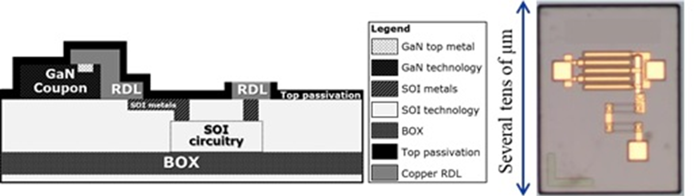
Fig. 1. X-FAB 3D integration proposal cross-section (left) and the picture of a GaN coupon (right).
This technique pushes the integration to transistor level as the dimension of the coupon can be as low as several tens of micrometers (see Fig. 1). Thus, we are considering it as monolithic integration.
Advantages for switch applications
This heterogeneous technology enables a smaller, cheaper and less complex circuitry than a system in package or a multi-chip module. It also helps getting a better control over parasitic elements and performance as we are pushing the integration into transistor level. Furthermore, this innovative integration technique combines the best of both GaN and RF-SOI technologies. It allows to:
• Benefit from the integration capabilities of CMOS,
• Overcome the availability and the co-integration difficulty of GaN on Si platform,
• Reduce the cost of the final circuit, as only few GaN devices are used where needed,
• Benefit from the high-power capability of GaN.
For example, an RF switch circuit typically needs control logic, Input/Output (IO) interface, and negative voltage generator in addition to the RF switching element. Gallium arsenide (GaAs), GaN, and P-type/Intrinsic/N-type (PIN) diode switches require in general separate CMOS die for the interface, negative voltage generator, and control logic. This constraint can also be avoided using the GaN on RF-SOI approach resulting in a monolithic circuit.
In addition to area saving, this heterogeneous integration improves GaN transistor intrinsic performance. The vertical isolation of the GaN on Si technology is poor compared to typical technologies used for switch applications such as RF-SOI. Some process techniques are developed to improve this isolation but they remain insufficient. By removing the substrate and putting the GaN coupon on RF-SOI the vertical isolation is significantly reduced as demonstrated in part III. As a consequence, the HEMT RF breakdown voltage should be improved [Reference Zhu, Klimashov, Roy, Blin, Whitefield and Bartle5].
Measurement setup and results
To validate our integration concept, a SPST switch has been designed for on-wafer small and large signal characterizations (see Fig. 2) [Reference Drillet, Loraine, Saleh, Lahbib, Grandchamp, Iogna-Prat, Lahbib, Sow and U'ren3]. It is composed of one GaN coupon containing two GaN HEMTs in series on a RF-SOI substrate. The GaN HEMTs have a gate length of 100 nm and a total gate width of about 1 mm. Integrated drain-source resistors of 1 kΩ as well as a 31 kΩ gate resistor are present to make the gate floating in RF. The GaN coupon is connected to the ground-signal-ground (GSG) pads on the RF-SOI wafer using the RDL. A DC pad is added to bias the gate.
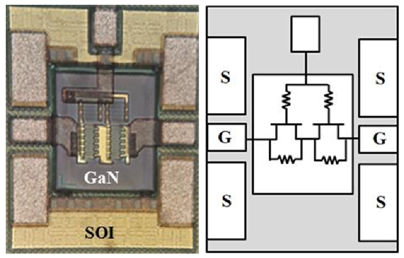
Fig. 2. Photograph (left) and schematic (right) of the RF GaN/RF-SOI SPST switch.
Small signal characterization
Insertion loss and isolation
The small-signal characterization of this heterogeneous device is performed from 0.2 to 30 GHz on the wafer with a Vector Network Analyzer. The reference planes of the measurement are at the tips of the probes. Then, the measurement results are de-embedded using open and short structures.
To evaluate the performance of this heterogeneous GaN/RF-SOI switch, its measurements were compared to the simulation of its equivalent in GaN/Si. This is due to the unavailability of GaN/Si equivalent structures. Nevertheless, previous characterization campaigns showed a good fit between simulation and experimental results for the GaN/Si transistors. The simulation of the GaN/Si SPST is done on a schematic reproducing the configuration of the GaN/RF-SOI sample. The gate resistor is 31 kΩ and the drain-source resistor is 1 kΩ. The dimension of the simulated GaN/Si HEMT is the same as the GaN/RF-SOI sample. For both cases, the gate length is 100 nm and the total gate width is about 1 mm.
The insertion loss is measured when the SPST switch is ON. It corresponds to a gate bias of 0 V as the GaN transistor is normally ON. The insertion loss comparison of measured GaN/RF-SOI and simulated GaN/Si is shown in Fig. 3. The heterogeneous structure presents lower insertion loss than the simulated GaN/Si switch, especially at high frequencies. This difference reaches indeed more than 1 dB at 30 GHz. Another interesting feature is that the insertion loss is flatter in measurement in the 0.2–30 GHz frequency band compared to the simulation. This behavior confirms the reduction of the vertical capacitive coupling to the substrate.

Fig. 3. Insertion loss comparison (left) and isolation comparison (right) of the measured GaN/RF-SOI SPST switch (dashed line), the simulated GaN/Si equivalent (solid line) and their respective RC equivalent models.
The isolation is measured when the SPST switch is OFF. It corresponds to a gate bias of −10 V. Fig. 3 shows the isolation comparison of the measured heterogeneous GaN/RF-SOI structure and the simulated GaN/Si switch. The results show similar behavior. We can still observe a difference in isolation level starting from 5 GHz.
Both of these figures show that this heterogeneous integration technique demonstrates similar small signal results compared to GaN/Si up to 3 GHz and much lower insertion loss at high frequency (>1 dB @ 30 GHz). Given the low insertion loss of the heterogeneous SPST, it could be resized to improve the isolation.
Vertical coupling reduction
As mentioned before, the vertical coupling is decreased in the heterogeneous GaN/RF-SOI thanks to the buried oxide of the RF-SOI. To quantify this vertical coupling reduction, a simple Resistor-Capacitor (RC) model has been built to fit both measured heterogeneous GaN/RF-SOI and simulated GaN/Si structures. In ON state, the channel behaves as a resistance R on. C sub represents the vertical coupling with the substrate (see Fig. 4). In OFF state the channel is closed. It is modelled by a capacitor C off and a resistor R off. The vertical coupling to the substrate is modeled by the capacitors C sub just like in ON state (see Fig. 4). The values used in this model for both ON and OFF states are given in Table 1.

Fig. 4. RC models of the GaN transistors in ON state (left) and in OFF state (right) for both substrate types.
Table 1. RC Models values for ON and OFF states GaN transistors for both substrates

The insertion loss and isolation given by the GaN/Si (simulation), the heterogeneous GaN/RF-SOI (measurement) and their respective RC models are shown in Fig. 3. This RC model is admittedly simple, but it still shows a good approximation of the small-signal behavior of the transistors in switching mode. This model also permits to have an approximation of the vertical coupling reduction. The capacitance C sub which represents this coupling in the model is 59% lower in GaN/RF-SOI compared to GaN/Si. The ON resistance values are similar for both cases but it seems that the ON resistance has been slightly over-estimated by the simulation. We expected the values to be identical in GaN/Si and GaN/RF-SOI. Besides the substrate coupling reduction, we can also observe an increase in C off. This increase is not expected and could be due to a process issue during the assembly phase of the GaN coupon and the RF-SOI wafer. This hypothesis is yet to be confirmed with further measurements.
Besides the flatter insertion loss versus frequency, the vertical coupling reduction should also improve the power handling of the switch. We use the formulas used by Zhu et al. [Reference Zhu, Klimashov, Roy, Blin, Whitefield and Bartle5] to evaluate the impact of the reduction of substrate coupling on the breakdown. In order to assess the accuracy of the breakdown voltage model, we plotted in Fig. 5 this model applied for GaN/RF-SOI, GaN/Si and RF-SOI switches, as well as RF-SOI switches measurement results. We can observe a very good correlation between this model and the measurements for the RF-SOI switches which gives us a good level of confidence in these equations.

Fig. 5. Breakdown voltage of the calculated RF-SOI (dotted), measured RF-SOI (half solid), calculated GaN/Si (dashed) and calculated GaN/RF-SOI (solid) switches versus the transistor stack height.
As we can also observe in Fig. 5, the substrate coupling reduction of the GaN/RF-SOI compared to the GaN/Si should also improve the breakdown voltage of the switches. It is especially true for large transistor stack heights. The calculated compression on the breakdown voltage occurs for a larger stack height for the GaN/RF-SOI technology compared to the GaN/Si.
Large-signal characterization
The large signal characterizations are performed at 900 MHz with an input power sweeping from 0 to 38 dBm. The continuous wave (CW) input signal is generated by a synthesizer, amplified by a power amplifier stage and filtered by a narrow band filter with 100 dB rejection. Thus, no harmonic components are injected in the device under test (DUT). At the output of the DUT, the signal is split into fundamental output power (Pout), second harmonic (H2) and third harmonic (H3) using three different filters centered to the three respective frequencies. The noise floor of the measurement setup is around −100 dBm.
Substrate non-linearity
As the substrate of the GaN/RF-SOI transistors is very different from Si-based ones, we characterized the non-linearity of this substrate on its own. To do so we have characterized the harmonics generated by the substrate through a CPW on GaN/RF-SOI (shown in Fig. 6) and compared it to a GaN/Si CPW.

Fig. 6. Photograph of the GaN/RF-SOI CPW.
There is no significant difference in terms of output power or insertion loss for the fundamental frequency. The second harmonic power levels (H2) and third harmonic power levels (H3) generated by the substrate and measured at the output for the GaN/Si and GaN/RF-SOI CPW are shown in Fig. 7 on the left and right, respectively.

Fig. 7. Measured H2 (left) and H3 (right) as a function of the input power (Pin) for the GaN/Si (solid lines) and the GaN/RF-SOI (dotted lines) for several CPW samples.
The second harmonic is 25–30 dB lower for GaN/RF-SOI compared to GaN/Si and the third harmonic is 30–40 dB lower. Both plots show that the linearity of the GaN/RF-SOI is significantly better than the GaN/Si. Thus, it proves that this integration technique allows significant improvements of the non-linearity contribution of the substrate.
Harmonic characterization of the SPST switch
The large-signal measurement results for the SPST switch shown in Fig. 2 are illustrated in Fig. 8. These results show that there is no compression up to 38 dBm as seen in the large signal insertion loss and Pout curves (Fig. 8 on the left). The measurement uncertainties are estimated at ± 0.1 dB. The H2 and H3 present 68 and 75 dBc rejection levels at 38 dBm, respectively (Fig. 8 on the right).

Fig. 8. Pout (dashed line) and insertion loss (solid line) (left) and H2 (dashed line) and H3 (solid line) (right) as a function of the input power (Pin).
Further measurements at higher power are planned to capture the 1 dB compression point (CP1), the RF breakdown voltage as well as the increase of H2 and H3 due to the power compression.
Conclusion
In this paper, we have presented the complete small and large signal characterization of a heterogeneous GaN/RF-SOI RF switch previously introduced in [Reference Drillet, Loraine, Saleh, Lahbib, Grandchamp, Iogna-Prat, Lahbib, Sow and U'ren3] as well as the impact of the substrate change on the GaN coupon. This innovative 3D approach enables the integration of RF-SOI MOSFETs and GaN HEMTs in the same chip. To validate this concept, samples were built and characterized on-wafer.
Our small-signal characterization has highlighted that GaN/RF-SOI samples present a 59% vertical coupling reduction thanks to the RF-SOI substrate. This reduction improves the small-signal behavior reflected in flat insertion loss: below 0.4 dB from DC to 30 GHz. Based on the equations in [Reference Zhu, Klimashov, Roy, Blin, Whitefield and Bartle5] and our RF-SOI switch data, it should also improve the RF breakdown of this SPST switch.
Our large-signal characterization has highlighted the superiority of the RF-SOI substrate in terms of linearity. The GaN/RF-SOI substrate on its own shows indeed a significant reduction of its non-linearity compared to standard GaN/Si, with an average of 30 dB reduction of H2 and H3. The breakdown of the SPST switch is beyond 38 dBm which is the maximal achievable power with our current characterization bench. At 38 dBm of input power H2 and H3 show respectively, 68 and 75dBc of rejection.
Characterizations at higher power are planned to determine the maximal power handling of this SPST switch. Moreover, a study for thermal dissipation is currently on-going for this innovative technique to assess the change in terms of thermal resistance and capacitance compared to GaN/Si as well as potential means to improve them. Our first characterizations show that the heat dissipation looks sufficient for low insertion loss switch applications. However, when higher power is at stake, good thermal management is mandatory. Overall, the GaN/RF-SOI results show better general performance compared to GaN/Si, except on the isolation, while allowing a higher level of integration.
Supplementary material
The supplementary material for this article can be found at https://doi.org/10.1017/S1759078721000076
Acknowledgement
We would like to acknowledge the Nano2022 program for partially funding this work.
 Frédéric Drillet received an engineering degree in electronics from the ENSEA in Cergy (France) in 2012 and received his Ph.D. degree in information and communication sciences and techniques from the University of Cergy (France) in 2016. He joined X-FAB in 2018 in the R&D department. His main research interest is the design of heterogeneous technologies for RF and millimeter-wave applications.
 Jérôme Loraine received an engineering degree in electronics from the ENSEA in Cergy (France) in 2014 and received his Ph.D. degree in information and communication sciences and technique from the University of Cergy (France) in 2019. He joined X-FAB in 2018 in the RF department as an RF designer where he is working on the development of heterogeneous technologies and RF-SOI designs.
 Hassan Saleh received his M.S. degree in micro-technologies and microwave architectures from INSA Rennes (France) in 2014. In 2017, he received his Ph.D. degree from Aix- Marseille University (France) where his research interest focused on electromagnetic scattering experimentation. In 2018, he joined X-FAB's research and development department to work on semiconductor devices and circuits characterization.
 Imene Lahbib received her Engineer diploma and M.S. degree in electronics in 2010 from ENSICaen and the University of Caen, France, respectively. She received her Ph.D. degree from the University of Caen, France, in 2014. Her Ph.D. is a collaboration between NXP Semiconductors and the Laboratory LaMIPS. Her research subject focused on RF BIST solution. In 2015, she joined X-FAB as RF designer. Her main research interests are the design and optimization of low noise amplifiers and switches. Since 2019, she is the team leader of the RF design team.
 Brice Grandchamp received a Ph.D. in Electronics from the University of Bordeaux (France) in 2007. After working for more than 10 years in RF III-V process and reliability, he joined X-FAB in 2018 in the RF Device & Process development Team to work on RF-SOI technology.
 Lucas Iogna-Prat received a degree in electrical engineering from the University of La Plata (Argentina) in 2013 and obtained a master in electronics from ESIEE (France). After working for several years as a researcher and IC layout engineer, he joined X-FAB France in 2018 as a device characterization and modeling engineer within the RF business unit.
 Insaf Lahbib received her M.S. degree in electronics in 2014 from the University of Caen, France. She received her Ph.D. degree from the University of Caen, France, in 2017. Her research subject focused on the analysis of aging effects of active components and integrated circuits under DC and RF constraints for a predictive approach. In 2017, she joined X-FAB as device reliability engineer.
 Ousmane Sow received his M.S. degree in electronics & Optical Microwave Technics in 2011 from Limoges University (France). After working for 4 years on spintronic analyzing and modeling and 3 years on microwave design circuits, he joined XFAB's RF-Design Team since January 2020.
 Albert Kumar received the B.S. degree in electrical engineering from UCLA in 2002. He has designed highly integrated analog and RF circuits at Maxim, Altera, and Qualcomm. Since 2017, he has been supporting customers designing in X-FAB's standard and advanced RF technologies.
 Gregory U'Ren received a Bachelor's degree in Physics from Hamline University in 1993, a Master's Degree and Ph.D. Degree in Materials Science and Engineering in 1997 and 2000 respectively, from the University of California, Los Angeles. He became a regular member of IEEE in 2002. His interests include high-speed microelectronics and optoelectronics. He has made significant contributions to the creation of high-performance SiGe BiCMOS technologies while at Conexant, subsequently Jazz Semiconductor until 2005. While at Qualcomm, he contributed to the development of MEMS-based reflective displays. Since 2010 he is based in Paris and has led the development of RF-SOI, SiGe, and GaN-based RF technologies at Altis Semiconductor, subsequently X-FAB.


 Open access