


1. Introduction
GaN and GaN-based alloys (AlGaN and InGaN) are attractive materials for the fabrication of blue and ultraviolet light emitting diodes and laser diodes due to their large direct band gap (1.9 eV for InN, 3.4eV for GaN, 6.2 eV for AlN) Reference Strite and Morkoç[1]. Previously, we reported the first GaN homojunctions and AlGaN/GaN heterojunctions Reference Zubrilov, Tsvetkov, Nikolaev, Soloviev and Dmitriev[2] which had an edge electroluminescence (EL) peak situated at 365 nm (300K). In this paper, we report on the optical properties of AlGaN solid solutions with AlN mole fractions in the range 0 - 30 % and AlGaN/GaN pn structures grown on 6H-SiC substrates by metalorganic chemical vapor deposition (MOCVD).
2. Experimental Procedure
AlGaN undoped epitaxial layers about 0.8 μm thick and AlGaN/GaN pn structures were on standard 30 mm 6H-SiC wafers by MOCVD Reference Dmitriev, Irvine and Edmond[3]. Epitaxial layers had smooth mirror-like surfaces. The crystal structure of the layers was described in Reference Nikitina and Dmitriev[4]. Mg and Si dopants were used for p- and n-layers, respectively, to control the carrier concentrations in the range from ~1 × 10¹⁶ to ~1 × 1019 cm−3. Carrier concentration was measured by mercury probe. Two types of structures were investigated: p-AlGaN/n-AlGaN heterostructures and p-AlGaN/GaN/n-AlGaN double heterostructures (DH). The AlGaN layers had AlN mole fractions up to 30 %. The AlGaN alloys used in the heterostructures had AlN mole fractions up to 10 %. The epitaxial layers and structures were characterized by cathodoluminescence (CL) and EL in the temperature range from 200 - 400K. While measuring, we eliminate the spectral sensitivity of our setup. For CL, excitation with a 4 - 15 keV electron beam was used. In AlGaN heterostructures, mesas 300 mm in diameter were formed by reactive ion etching Reference Vassilevski, Sizov, Babanin, Melnik and Zubrilov[5]. In AlGaN/GaN DHs, 20 × 500 μm mesa stripes were formed. A vertical device geometry was employed. Pd and Ni were used as top and bottom ohmic contact metals to p-GaN and n-SiC, respectively. The location of pn junctions in the heterostructures was determined by simultaneous detection of electron beam induced current (EBIC) and back scattered electron (BSE) signals in a scanning electron microscope.
3. Results
Edge CL peaks for AlGaN layers with various AlN mole fractions are shown in figure 1. An increase of the AlN mole concentration leads to a “blue” shift of the edge peak position, alloy broadening and a reduction in CL intensity. The dependence of the edge peak energy position on the AlN mole fraction (x) is shown in figure 2. Curve 1 corresponds to linear band gap energy approximation E(x)=3.4(eV)+2.8(eV) x and curve 2 depicts the approximation: E(x)=E(0)+ax+bx 2 where E(0) = 3.4 eV, a = 2.19 ± 0.16 eV, and b = 0.65 ± 0.14 eV.
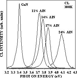
Figure 1. CL spectra for AlGaNlayers with various AlN concentrations
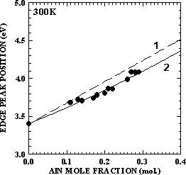
Figure 2. Dependence of the CL edge peak position on AlGaN composition
BSE and EBIC signal profiles across a p-Al0.05Ga0.95N/n-Al0.03Ga0.97N heterostructure are shown in figure 3. The minimum in the BSE signal corresponds to the alloy layer in the structure. The CL spectrum (figure 4) has two short wavelength peaks corresponding to carrier recombination in p- and n-AlGaN regions. In the EL spectrum (figure 4), only the n-AlGaN-related peak was observed. The peak position corresponds to carrier recombination in the narrower bandgap n-AlGaN region. In both spectra the edge luminescence from the GaN region (λmax ~ 365 nm) was also observed. The fact that the EL spectrum contains a peak situated at 365 nm means that holes injected into the n-AlGaN region of the pn junction reach the n-GaN layer and recombine there. It was found that the photon energy for the EL edge peak measured from AlGaN pn junctions follows the same compositional dependence as the CL edge peak does.

Figure 3. EBIC and BSE signal profiles across the p-AlGaN/n-AlGaN heterostructure
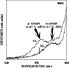
Figure 4. EL and CL spectra for the structure shown in figure 3
A typical EL spectrum taken under dc conditions on a DH having a GaN active layer is shown in figure 5. The edge peak was detected at 365 nm. The full width at half maximum (FWHM) of the edge peak was 86 meV (300K). The impurity related emission in the wavelength range from 400 to 450 nm and the so-called “defect” emission at ~550 nm are also presented in the spectra Reference Zubrilov, Tsvetkov, Nikolaev, Soloviev and Dmitriev[2]. As the temperature is increased, the edge emission peak shifts to longer wavelengths, its FWHM increases, and intensity falls off (figure 6). The temperature dependence of the EL edge peak energy position was almost the same as that determined previously for the PL edge peak of GaN layers grown on SiC Reference Zubrilov, Nikolaev, Tsvetkov, Dmitriev, Irvine, Edmond and Carter[6].
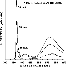
Figure 5. EL spectra of a p-Al0.08Ga0.92 N/GaN/n-Al0.02Ga0.98N DH at various forward currents
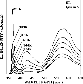
Figure 6. EL spectra of the DH shown in figure 5 in the temperature range from 300 - 360K
We may conclude that AlGaN/(AlIn)GaN heterostructures having an edge EL peak at a wavelength corresponding to near band gap recombination in the active region of the structure can be grown on SiC substrates.
Acknowledgments
The authors thank K. Vassilevski and V. Sizov for mesa fabrication by plasma etching and E. Kalinina and N. Seredova for help in sample preparation. A. Zubrilov and D. Tsvetkov also thank the Russian Foundation of Fundamental Research (contract number 95-02-04148-a) for financial support.


