


Introduction
Within materials characterization by electron microscopy, energy-dispersive X-ray spectroscopy (EDX) is the most widespread method for compositional analysis. For quantitative analysis in the scanning transmission electron microscope (STEM), i.e. to determine the stoichiometry of the analyzed volume, the Cliff–Lorimer ratio technique has been the most commonly used method (Cliff & Lorimer, Reference Cliff and Lorimer1975). The method relates the intensity of the detected X-rays to the composition of the elements in a multi-component system through a set of sensitivity factors, the so-called k-factors, assuming a thin specimen with negligible absorption effects. The k-factors can be determined experimentally using well-characterized, multi-element standards. Alternatively, calculated factors provided at the installation of the detector can be used, which is more user friendly. The latter is, to date, practically the default approach despite its known lack of accuracy. Absorption correction is possible within this ratio technique but requires knowledge of specimen thickness, absorption path, and detector conditions, which is challenging to determine accurately. The more recently introduced ζ-factor method for EDX quantification (Watanabe & Williams, Reference Watanabe and Williams2006) resolves two main drawbacks of the Cliff–Lorimer approach. First, pure-element standards can be used; an improvement compared to the ratio technique where the absence of suitable standards can be a limitation. Second, the mass thickness is determined simultaneously as the composition, enabling an easy, built-in absorption correction. However, the drawback of the approach is that to determine the sensitivity factors, called ζ-factors, the thickness of the standards must be known. In addition, the probe current must be measured, adding a step in the acquisition process. Due to these practical challenges, the ζ-factor approach, despite its clear advantages, is not incorporated into most commercial systems and is therefore not as widely applied as the k-factor method. Building further on the ζ-method, other approaches have been suggested such as the cross-section method (MacArthur et al., Reference MacArthur, Slater, Haigh, Ozkaya, Nellist and Lozano-Perez2016), linking the sensitivity factors to physical cross-sections. However, the method also inherits the same limitations as the ζ-method.
Independent of the used approach, accurate quantification requires the correct determination of sensitivity factors. As stated, this can be a challenging exercise, potentially more so than the actual measurements. In multi-element standards, the sensitivity factors will be dependent on the relative absorption of different elements. To obtain meaningful sensitivity factors, ideally the standards should have no or similar absorption conditions as the volume to be analyzed. Correctly accounting for the absorption effects is, however, very tedious. The possibility of using pure-element standards in the ζ-factor determination reduces this problem to only include self-absorption. Most K- and L-lines have 5% or less self-absorption at 30 nm specimen thickness, and Watanabe and Williams argue that this is low enough for an accurate quantification (Watanabe & Williams, Reference Watanabe and Williams2006). However, if a better precision is desired, or for the analysis of light element K-lines, many L-lines, and most M-lines, much thinner standards are needed. This might induce a challenge to get enough counts for a statistically sound determination of ζ-factors.
If the determined sensitivity factors are not absorption free, or they do not reflect an equal amount of absorption, applying absorption correction will not make the right corrections to the composition. In addition, the absorption correction routine itself, which is made available through e.g. open-source libraries (de la Peña et al., Reference de la Peña, Prestat, Fauske, Burdet, Jokubauskas, Nord and Garmanslund2019), also has limitations. The absorption of X-rays is dependent on the density and path length on the way out of the specimen. In a regular absorption correction routine, the specimen is assumed to be flat with uniform composition. However, for a multi-component system, the density of the material through which the X-rays must be transmitted before reaching the detector will often be nonuniform and is not easily modeled. Additionally, the thickness must be determined accurately for the specimen (k-factors) or for the standards (ζ-factors). If not assessed correctly, both the composition and output thickness (for the ζ-method) will be wrong and the subsequent absorption correction and thus quantitative analysis incorrect.
Several alternative methods have been developed that address the problematic issues with the use of sensitivity factors such as accuracy and practicalities, e.g. effective k-factors (Walther & Wang, Reference Walther and Wang2016), extrapolated k-factors (Parisini et al., Reference Parisini, Frabboni, Gazzadi, Rosa and Armigliato2018), and composition related to principal components (Rathi et al., Reference Rathi, Ahrenkiel, Carapella and Wanlass2013). Common for the methods is that they require advanced simulation tools and/or need standards with known thickness. Although addressing issues of common quantification routines, they seem not to be applied by a broader user group. To become appealing to the average EDX user, the quantification method should, in addition to being accurate, be easy to apply and understand. The input parameters needed for quantification should be readily available, preferably within the specimen. The latter is the most stringent requirement, as a reference is always needed for calibration to achieve the most accurate quantification results. However, if a proper reference area within the specimen is lacking for one of the elements, its composition can for certain material systems be determined by using a constraint on the composition of one of the other elements. This is the case for systems with ternary semiconductor compounds, where the stoichiometric relationship gives that the composition of one of the elements will be constant. Ternary semiconductors constitute a technically important group of materials with a need for accurate composition determination to understand and optimize their optoelectronic properties and is thus an important system for improved quantification accuracy.
In this paper, a method is outlined to determine the composition internally within the specimen of ternary semiconductor compound heterostructures, where a known binary reference within the scan area can be used for easy-to-use composition analysis of the ternary area. Making use of a known internal composition ratio can also be used as an alternative quantification method in electron energy loss spectroscopy (Bashir et al., Reference Bashir, Gallacher, Millar, Paul, Ballabio, Frigerio, Isella, Kriegner, Ortolani, Barthel and MacLaren2018). In the present work, the method of internal composition determination (ICD) does not require any external standards or absorption correction. The principle behind it is an iterative optimization routine, which minimizes composition fluctuations in the element which should be of constant composition (e.g., As in AlxGa1−xAs). Thereby, absorption between the elements, as well as by the surrounding areas, is included in the quantification. The method is tested on three different heterostructured ternary systems; AlGaAs/GaAs, GaAsSb/GaAs, and InGaN/GaN. In addition to representing technically important systems, they are suited to evaluate the effect of atomic number (and hence absorption). Different specimen geometries are also considered. The results are compared to conventional quantification methods.
Materials and Methods
Internal Determination of Composition
The method is developed based on the ζ-method where the composition determination is refined through an iterative process, incorporating the known composition relation that one element has a constant composition. This element is called the benchmark element. The assumption is that the absorption of the elements in a given reference area is similar to the absorption in the region of interest. An arbitrary input thickness and probe current/dose can be used, returning a relative thickness profile of the region of interest, which can be used as validation. A relative thickness profile means that the shape of the profile is reconstructed, but the absolute thickness of the analyzed area will only be found if the input thickness of the reference area is correct. A flow chart of the method is given in Figure 1. Relative ζ-factors are calculated for two of the elements based on their intensities in the binary reference area. A ζ-factor relates the measured intensity I to the composition C, and is proportional to the mass-thickness ρt and total electron dose D. For a reference area containing two elements A and B with known composition CA and CB, their relative ζ-factors can be calculated using
 $$\zeta _A = \displaystyle{{\rho tC_A^r D} \over {I_A^r }}{\rm \;and\;}\zeta _B = \displaystyle{{\rho tC_B^r D} \over {I_B^r }}, \;$$
where the superscript r denotes the intensity and composition of the reference area. If the ζ-factors for all the relevant elements are known, the composition of the benchmark A in the area of interest a is given by
 $$C_A^a = \displaystyle{{\zeta _AI_A^a } \over {\mathop \sum \nolimits_j^N \zeta _jI_j^a }}, \;$$
and similarly for the other elements. The unknown ζ-factor for the third element C in the ternary system (AB 1−xCx) is determined so that it gives the least fluctuations in the composition of the benchmark element. The simultaneous iteration of reasonable values for the ζ-factor and a flatness criterion for the fluctuations of the composition CA of the benchmark element ensure a ζ-factor that gives the lowest possible fluctuations. Flatness is here defined as the difference between the composition maxima and minima of the benchmark element. If the reference area and area of interest are within the same scan area, ρt and D can be assumed to be the same for all ζ-factors, and equation (2) can be expressed as
 $$C_A^a = \displaystyle{{( C_A^r /I_A^r ) I_A^a } \over {\mathop \sum \nolimits_j^N ( C_j^r /I_j^r ) I_j^a }}.$$
Fig. 1. Flow chart of the internal determination of ζ-factors, where one of the elements of the system, CΑ, is known to be constant. First, ζ-factors are determined from one or more reference areas of known composition. Then, one iterates over a set of reasonable ζ-factors (0–10ζ Α) while simultaneously iterating over a flatness criterion starting at 0, finding the ζ-factor that gives the smallest possible fluctuations of CΑ.
It can be shown by considering the definition of the k-factor and that the composition of all elements adds up to one that this is effectively the same as determining k-factors internally within the specimen, where the thickness and dose are not needed. However, by using zeta factors, the relative output thickness profile is returned as
 $$\rho t = \displaystyle{{\mathop \sum \nolimits_j^N \zeta _jI_j} \over D}.$$
The deduced mass thickness can be used as a validation of the quantification results by comparing the profile to the expected thickness profile, for example, flat for a parallel FIB lamella. Optimizing the ratio C/I instead of the ζ-factor could also be used in the algorithm, e.g. when dose measurements are not available.
Experimental Procedures
Three different ternary III–V compound heterostructure systems are chosen to test the method (see Table 1). All samples were grown as nanowires with molecular beam epitaxy (MBE) through either a catalyst-induced (arsenides) or catalyst-free (nitrides) method. The nanowires contain both an area of pure binary compound (either GaAs or GaN) which is used as a reference area, and an area to be analyzed with varying concentrations of the third element (Al, Sb, or In). Sample 1 is a GaAs/AlGaAs core–shell nanowire where Al has segregated into bands of varying Al concentrations in the shell. The nanowire is cut perpendicular to the growth direction (i.e., in the [111] direction, see inset in Fig. 2) by focused ion beam (FIB) and the GaAs core is used as a reference area. Sample 2 is an FIB cross-section along a nanowire containing several GaAs1−xSbx superlattices with GaAs spacers between. The nanowire is cut in the [ $\bar{1}\bar{1}2$] direction as shown in the inset of Figure 3a. Further growth details and characterization for Samples 1 and 2 can be found in Nilsen et al. (Reference Nilsen, Reinertsen, Mosberg, Fauske, Munshi, Dheeraj, Fimland, Weman and van Helvoort2015) and Ren et al. (Reference Ren, Ahtapodov, Nilsen, Yang, Gustafsson, Huh, Conibeer, van Helvoort, Fimland and Weman2018), respectively. Sample 3 is also MBE grown. The analyzed nanowire was grown at 620 C for 1 h and fluxes for In, Ga, and N2 were 0.1, 0.2, and 2.7 Ml/s, respectively. The substrate with the as-grown nanowires was scratched to break off the nanowires, which were subsequently dispersed on C-coated 300 mesh Cu grids. Thus, for sample 3, the nanowire is analyzed in the [ $\bar{1}10$] projection as indicated in Figure 5c. In this case, no FIB preparation is applied as with the other discussed specimens.
Table 1. Overview of the Samples Used to Test the Method.


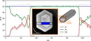
Fig. 2. Internal determination of the compositioin of the GaAs/AlGaAs core–shell nanowire in a cross-section perpendicular to the growth direction as depicted in the inset, showing the composition of the core and two of the facets. The result is compared to quantification using calculated k-factors (lighter color). The inset shows a high-angle annular dark-field (HAADF) STEM image of the specimen, indicating from where the data were acquired. The blue region indicates the reference area.

Fig. 3. (a) HAADF STEM image of parts of the GaAs/GaAs1−xSbx nanowire showing the top three superlattices. The scan area and the reference area (blue) are indicated. The inset on the right depicts the specimen geometry. (b) Internal determination of the composition of three superlattices, compared to quantification using calculated k-factors (lighter color) at a tiltx = −14.2 away from the detector. (c) Internal determination of the composition of the top three GaAsSb inserts of the top superlattice compared to calculated k-factors at a tiltx = +15° towards the detector. (d) The same data as in (b), cropped to about the same area as in (c), and compared to the nondenoised data (lighter color).
The specimens were examined on a double-corrected JEOL ARM 200F at 200 kV using a double tilt reinforced holder. The TEM is equipped with a single Centurio SDD EDX detector with a nominal solid angle of 0.98 str and an elevation angle of 24.3°. The specimens were oriented edge on the heterostructure interfaces for optimum spatial resolution and tilted along the interfaces away for a major zone axis to avoid channeling conditions. The beam current was measured before and after each data acquisition using the built-in Pico ampere meter of the Gatan Image Filter (GIF) drift tube, which can measure probe currents down to the pA range. The spectrum images were acquired using the strongest condenser lens setting typically used for analytical work, the so-called 3C probe for JEOL ARMs and 50 μm aperture which results in a probe size of 0.15 nm. Pixel times (i.e., the time at each probing position) of 0.05–0.1 s were used. Line scans were created by summing up the short axis in the 2D spectrum image. The thicknesses used in ζ-factor determination were found either by measuring t/λ using electron energy loss spectroscopy (Egerton, Reference Egerton2011), where the mean-free-path λ was estimated based on work by Malis et al. (Reference Malis, Cheng and Egerton1988), or by considering the projected width of the nanowires. All analyses of raw EDX data were done either by using the open-source, python-based library HyperSpy (de la Peña et al., Reference de la Peña, Prestat, Fauske, Burdet, Jokubauskas, Nord and Garmanslund2019) or by self-developed code written in python. The X-ray intensities are extracted using an integration window of 1.2 times full-width half-maximum and the background is subtracted using background windows as implemented in HyperSpy. For comparison, quantification was also performed using calculated k-factors supplied by the microscope manufacturer. Absorption coefficients as listed by Chantler et al. (Reference Chantler, Olsen, Dragoset, Chang, Kishore, Kotochigova and Zucker2005) and implemented in HyperSpy combined with absorption correction terms calculated based on the formula of Philibert (Reference Philibert1963) are used to interpret the data. All compound densities are calculated in HyperSpy. Unless otherwise stated, denoising based on principle component analysis (Carter & Williams, Reference Carter and Williams2016) was applied as a first step in the data analysis. A tutorial Jupyter notebook with the code developed herein, as well as example data, is made available on GitHub (Nilsen, Reference Nilsen2019) for readers who are interested in further details as well as applying the presented method to their own data.
Results and Discussion
Sample 1: GaAs/AlxGa1−xAs
With the first sample, the proposed method is tested for the case of a light element (here Al) replacing a specific heavy element (here Ga) in a binary compound (GaAs). GaAs/AlxGa1−xAs is an interesting system because AlKα is heavily absorbed by both Ga and As (Table 2). In an AlxGa1−xAs compound, Al replaces Ga in the lattice, making As the benchmark element. Figure 2 shows the internally determined composition distribution of the core–shell structure for two out of six facets. K-lines are used and Ga and As concentrations of 50 at% each in the core (reference) region are assumed (38–93 nm, blue area in Fig. 2). The result is compared to quantification with calculated k-factors (lighter color), and at the point of maximum Al concentration, the difference is 3.9 at%. When using Cliff–Lorimer with calculated k-factors (without absorption correction), the As composition profile fluctuates with the Al content by more than 2 at%. This effect can be explained by the fact that AsKα is more absorbed by Ga than Al (Table 2), so that a decrease in Ga concentration (when replaced by Al) increases the AsKα signal. This changes the ratio between the GaKα and AsKα signals and thus the determined composition.
Table 2. Mass-Absorption Coefficients in cm2/g of Ga, As, and Al for the X-ray Lines GaKα, AsKα, and AlKα (Chantler et al., Reference Carter and Williams2005).

By considering the absorption correction terms for the X-ray lines at this specimen thickness (45 nm) and tilt towards the detector (3.3°), which are calculated by assuming a uniform composition in the absorption path, the absorption of the relevant X-ray lines in a compound with composition Al0.35Ga0.15As0.5 should be 10.7, 0.2, and 0.1% for AlKα, AsKα, and GaKα, respectively. This composition is chosen as it is the maximum Al composition in the specimen as determined by the method presented in this paper and will exhibit the most pronounced absorption effects. Since the absorption of AsKα and GaKα is negligible, the compositional change due to absorption at this point should be about 2.8 at% for Al, 2 at% for As, and 0.6 at% for Ga. This is close to the observed differences between the calculated k-factors and internal determination of composition. The improvements in the quantification are in line with calculations. Furthermore, it is illustrated, given the assumptions made, how the absorption correction is directly included in the quantification step of the presented method, without the need of knowing the thickness of the specimen.
Sample 2: GaAs/GaAs1−xSbx
In the axially heterostructured Sample 2, the group III element Ga is the benchmark element, and the third element Sb is heavier than both elements in the reference area. Figure 3b shows the quantification of the top three superlattices of the Sb-containing nanowire using the GaKα, AsKα, and SbLα lines. Here, the top 350 nm were used as a reference area (blue area in Fig. 3a), where the Sb concentration should be close to zero, and the Ga and As concentrations were assumed to be 50 at% each. The lighter colored lines show the quantification with calculated k-factors. In order to exaggerate absorption effects, the data are acquired at a specimen holder tilt of x = −14.2°, i.e. away from the detector. This is effectively reducing the solid angle due to shadowing by the holder. Note that the y-tilt does not matter for this experimental set-up, as the detector is mounted perpendicular to this direction (Watanabe & Wade, Reference Watanabe and Wade2013). The difference in maximum Sb content of the superlattices is about 2 at% for the two quantification methods. More strikingly is that the Ga concentration varies in phase with the Sb content by 1.3 at% for the calculated k-factors. This is opposite to what is seen in the intensity profiles, where the GaKα signal varies in phase with AsKα. GaKα is more absorbed by Sb than by As (see Table 3), so when the Sb content increases, the detected GaKα signal decreases. On the other hand, SbLα is more absorbed than AsKα, so the SbLα signal does not increase sufficiently to compensate. This difference in absorption between the different lines causes a change in the ratios giving an overestimation of the Ga content using calculated k-factors.
Table 3. Mass-Absorption Coefficients in cm2/g of Ga, As, Sb, and Pt for the X-ray Lines GaKα, AsKα, and SbLα (Chantler et al., Reference Carter and Williams2005).

In Figure 3c, the specimen is tilted to x = +15°, i.e. towards the detector. Here, the absorption is less prominent, and the quantification with calculated k-factors gives an almost identical result for the Sb concentration. The Ga profile shows no fluctuations with the variation in Sb content. When tilting the specimen from x = −14.2° to x = +15°, the change due to absorption is calculated to be 0.6, 1.3, and 5.7% for GaKα, AsKα and SbLα, respectively (Fig. 4). However, this should only give very small changes in the measured composition between the two tilts, equivalent to about 0.2 at% for Ga, 0.01 at% for As, and 0.4 at% for Sb in the point of maximum Sb composition. On the other hand, the absorption path length for an 83 nm thick specimen in our detector set-up is changed from 131 nm at tiltx = +15° to 473 nm at tiltx = −14.2°. Since the data are acquired with the detector perpendicular to the side of the nanowire (see Fig. 3a), the absorption path will pass through some of the Pt protection layer from the FIB specimen preparation routine. As seen in Table 3, the absorption coefficient for SbLα in Pt is very high, which explains the severe absorption. It also illustrates the possible problematic nature of regular absorption correction. Since the composition along the absorption path is not uniform, regular absorption correction is inadequate. With the internal determination of composition, the absorption path towards the detector does not need to be known. The method is robust as it gives very similar quantification results regardless of specimen tilt.

Fig. 4. The absorption correction for the GaKα, AsKα, and SbLα lines as a function of stage tilt in a compound with concentration Ga0.5As0.42Sb0.08. The specimen thickness is 83 nm and an elevation angle of the detector 24.3°.
Sample 3: GaN/InxGa1−xN
In the two previous examples, the internal determination of composition was shown to work for the binary compound GaAs when the group III element is replaced with a lighter element (Al) and when the group V element is replaced with a heavier element (Sb) in FIB-prepared, flat specimens. In the final test case, a GaN nanowire with In-rich quantum wells, the benchmark element N is with its low X-ray energy (0.39 keV) prone to absorption. In addition, the thickness is varying along the extracted nanowire. Figure 5b shows the internally determined composition of four successive quantum wells compared to the quantification result using calculated k-factors. Using a reference as indicated in Figure 5a (blue) with an assumed composition of 50 at% Ga and 50 at% N, the maximum In content is found to be 8.5 at% in the fourth well, more than 2 at% higher than with calculated k-factors. As with the previous examples, the benchmark element N fluctuates, now in phase with the In content when using calculated k-factors, explained by higher absorption of NKα by Ga than by In (Table 4).

Fig. 5. (a) HAADF STEM image of part of the GaN nanowire with InxGa1−xN quantum wells. The marked area indicates the scan region; blue indicates the reference area. (b) Internal determination of composition compared to quantification with calculated k-factors (lighter color). (c) Schematic depicting the specimen geometry. (d) Corresponding relative thickness profile, when the thickness of the reference area was set to be 59 nm.
Table 4. Mass-Absorption Coefficients in cm2/g of In, Ga, and N for the X-ray Lines InLα, GaKα, and NKα (Chantler et al., Reference Carter and Williams2005).

The absorption path length of a nanowire is different from that of flat specimens. In addition, the cross-section of nanowires often deviates from a perfectly hexagonal symmetry (Heilman et al., Reference Heilman, Munshi, Sarau, Göbelt, Tessarek, Fauske, van Helvoort, Yang, Latzel, Hoffmann, Conibeer, Weman and Christiansen2016), e.g. as seen for the nanowire in Figure 2. Below, we assume that the detector is approximately perpendicular to the side of the nanowire (see Fig. 5c) and that the absorption path length can be set to half the projected width of the nanowire. Under this assumption, the absorption path length in the reference area is 34 nm, and the change due to absorption of NKα in GaN should be 8%. Using calculated k-factors, the offset of N from the expected value of 50 at% in the reference area is 5 at%. This equals an absorption path length almost double the estimated path length and thus longer than the width of the nanowire. Despite the uncertainties in the estimations, this indicates that the calculated k-factors are not correct with respect to each other. This is substantiated by the fact that absorption of NKα should cause a small increase in the determined In content. Here, calculated k-factors underestimate the In content, pointing at an additional source of the observed deviation than only absorption effects.
The thickness of the nanowire varies over the scanned area. This is seen from the corresponding thickness map in Figure 5d, which is generated by assuming a thickness of 59 nm ( $\sqrt 3 /2$ of the projected thickness, assuming a symmetric hexagonal cross-section) in the reference area. This gives a difference in thickness from top to bottom of 15 nm, slightly more than the 11 nm that is estimated from the projected thickness. This confirms that the nanowire is not hexagonally symmetric and that the thickness estimation is imprecise. Analyzing a larger area caused the method to fail, as the change in absorption due to thickness change was too large. Ideally, external sensitivity factors with regular absorption correction should in this case give a more reliable result if the absorption path and absorption-free sensitivity factors (i.e., determined without any significant absorption in the standards) can be determined accurately. However, since fulfiling these two criteria might be challenging if not impossible, ICD as developed here is a good and easy alternative if the change in thickness is limited over the scan area.
Confidence Considerations
The uncertainty of the internally determined composition using the method outlined in this paper is reflected in the final flatness criterion of the algorithm, i.e. the variation in the determined composition known to be constant. The method is sensitive to three characteristics of the specimen/experiment: (1) changes in thickness or other factors causing a large change in absorption conditions, (2) changes in channeling conditions affecting the intensity ratios, and (3) the noise level in the signal. If the changes due to absorption are smaller than the noise level of the X-ray line of the element with constant composition, the algorithm might not be able to correct this. Principal Component Analysis (PCA) is often used as a denoising routine for EDX data (Williams & Carter, Reference Williams and Carter2009). In Sample 1, the noise level of the As composition profile was ±2 at% of the average value. If denoising the data with PCA, the noise level was ±0.1 at%, but the maximum Al content was lowered by 1 at% which is within the noise level of the raw data. When comparing the X-ray counts for raw and denoised data, the latter seem like a good representation of the raw data. Thus, in this case, the denoised data are judged to give a reliable result.
In the data of Sample 2 acquired at tiltx = −14.2°, absorption and shadowing by the specimen holder cause lowered counting statistics and thus a poorer signal-to-noise level. Using raw data, the noise of the Ga composition profile amounted to about ±3 at% from the average, while for denoised data, it was ±0.1 at%. However, determining the composition internally gives conforming results both for raw and denoised data, which is seen in Figure 3d. When the specimen is tilted towards the detector, the noise level in the raw data is much smaller (<±1.5 at%), in line with the common understanding that counts are of primary importance when quantifying. Here, ICD gave a maximum Sb content about 1 at% higher than for denoised data and when quantifying using calculated k-factors. Again, the discrepancy between the quantifications is within the noise level of the raw data. Since the two latter methods are coinciding, and denoising does not change the ratios in the X-ray counts, the quantification result of denoised data is deemed reliable.
For Sample 3, the counting statistics for the NKα X-rays is poor due to the high absorption of the low-energy characteristic X-rays in the specimen. In addition, the thickness change along the scanned area causes a change in the absorption conditions for NKα of about 5%. Using ICD on raw data, the fluctuations of the composition profile of the benchmark element N are about ±3 at% around the mean value. The maximum In content is about 0.5 at% lower than when using denoised data, but from the profile, it is clear that the iterative algorithm has not been able to compensate for the absorption effects. On the other hand, it is still an improvement from the quantification with calculated k-factors, even if it falls short when the noise level is too high. In summary, denoising the data helps the algorithm to work better as high noise levels might inhibit the algorithm to find the optimum zeta factor value.
Besides the uncertainties due to changes in absorption conditions and intensity ratios, there are two main sources of error when determining the composition internally within the specimen. The first and most crucial is the X-ray counting statistics, which is a general challenge with EDX of thin specimens regardless of what quantification procedure is applied. The second is the assumed composition and counts of the reference area. For the reference area, the counts are summed over all pixels, thus the counting statistics are greatly improved. The highest error is for the GaN reference, where the relative error for GaKα and NKα is 0.8 and 2%, respectively. For Samples 1 and 2, the reference area used has a relative error less than 0.5%. A possibly larger source of error is the assumed composition of the reference area. In this study, we have assumed a composition of 50 at% for the elements of the binary compounds. This is a reasonable assumption for whole nanowires if far from the heterostructured interfaces. For FIB-prepared specimens, on the other hand, the composition might have been altered due to Ga implantation from the ion beam during specimen preparation. This can be a problem if Ga is the element being replaced in the binary compound as in sample 1. However, here the potential Ga implantation can be assumed to be equal throughout the specimen, including the reference area. Its contribution to the final result can thus be neglected because implantation is incorporated in the quantification via the internal reference. The errors in the determined composition of denoised data for selected values of the two quantification methods are summarized in Table 5. The error is determined by fitting a Gaussian shape of the X-ray intensity peaks in the spectrum using a 99.7% confidence interval. An error of up to ±20% in the calculated k-factors is assumed, which is the case for some characteristic X-rays (Williams & Carter, Reference Williams and Carter2009). Errors in the PCA components were not taken into account (Hellton & Thoresen, Reference Hellton and Thoresen2014). The results show that when the error due to counting statistics is low, the internally determined composition gives a great improvement in precision compared to calculated k-factors, although the true error on calculated k-factors may be smaller than that assumed here.
Table 5. The Determined Composition in at% Together with the Absolute Error with a 99.7% Confidence Interval of the Denoised Data of the two Quantification Methods; Internal Composition Determination (ICD) and Using Calculated k-factors (CL).

Conclusions
Here, a method is developed for determining the composition of heterostructures based on internal references, i.e. areas of known composition within the scanned region of the EDX data. The analysis of three different ternary III–V heterostructured samples found that the new method is more robust than the commonly used CL method as absorption effects are accounted for without the need of determining the absorption path. For all three samples, a suitable reference for one of the elements was lacking. By assuming a constraint that one of the elements has constant composition throughout the scanned area, e.g. the benchmark element As in AlxGa1−xAs, the composition of the third element was determined by minimizing the composition fluctuations of the benchmark element. When the reference area is used as an internal standard, only one set of compositions will minimize the fluctuations of the benchmark element. The method can, to a certain degree, handle absorption due to a inhomogeneous absorption path which otherwise would be difficult to quantify and where regular absorption correction would be insufficient. If the absorption is constant throughout the area of analysis, the main source of error is the counting statistics, which is an inherent problem of EDX analysis itself. The method should be applicable to any material system, not just compound semiconductors, that has a suitable internal reference and a boundary condition in the form of a constant benchmark element over the area of interest. In those cases, ICD is an easy alternative to using the Cliff–Lorimer method with calculated k-factors and without the need for special standards. It should be an improved and simplified method for EDX quantification.
Acknowledgments
Dr. Mazid Munshi and Dr. Dingding Ren are acknowledged for growing the nanowire samples. Daniel Lundeby is acknowledged for coming up with the idea of tuning ζ-factors. The Research Council of Norway is acknowledged for the support through the programs NANO2021 (Grant nr. 239206/O70), NorFab (Grant nr. 197411/V30), and NORTEM (Grant nr. 197405).


 Open access