


Introduction
Imaging and analysis techniques involving transmission of electron beams through thin specimens provide information that can be difficult, if not impossible, to obtain otherwise. This characterization approach has traditionally been applied only within dedicated transmission electron microscopes (TEMs) designed to operate at accelerating voltages from 60 to 300 kV. These voltages are high enough to ensure specimens with thicknesses of 10s to 100s of nanometers are essentially transparent, that is, beam-sample interactions are almost negligible [Reference Williams and Carter1].
On the opposite extreme are scanning electron microscopes (SEMs) designed to examine large areas of material surfaces using accelerating voltages from 0.2 to 30 kV (that is, 10s to 100s of times lower than TEMs). Analyzing bulk specimens at lower voltages results in complete absorption of the incident beam, thereby enabling use of imaging and analysis techniques very different from but complementary to those available in TEMs [Reference Goldstein2].
Despite the stark differences between these types of instruments, recent years have seen increased adaptation of transmission-based techniques for use in SEMs, including scanning-transmission electron microscopy (STEM) imaging, low-energy nanodiffraction [Reference Schweizer3], transmission Kikuchi diffraction [Reference Keller and Geiss4], and even electron energy loss spectroscopy (EELS) [Reference Yamazawa5]. Since SEMs are often more financially and logistically accessible for smaller laboratories, development of crossover techniques enables a wider range of researchers to collect information obtainable only via transmission experiments.
However, conducting these experiments at SEM voltages results in substantially different interactions between the electron beam and the sample compared to typical TEM conditions. This has important consequences for data collection and analysis, especially in the context of energy dispersive-X-ray spectroscopy (EDS, EDX, or XEDS). Although EDS analysis is common in both SEMs and TEMs, there is little published guidance on how to apply this technique to freestanding films analyzed at 30 kV and below [Reference Watanabe and Williams6].
Decades of research have produced a robust library of theory-driven semi-empirical guidelines for EDS analysis under many different conditions [Reference Boona7–Reference Friel9], including analysis with and without standards. To briefly summarize this extensive body of work:
• SEM models generally assume full beam absorption and account for backscattering, X-ray absorption, and secondary fluorescence with element-dependent matrix corrections (“ZAF”) where Z refers to the atomic number, A to self-absorption of the X-rays dependent on sample characteristics, and F to fluorescence [Reference Goldstein2]. More nuanced models exist to account for other factors, including irregular geometries [Reference Newbury and Ritchie10], thin films on substrates [Reference Waldo11], and variable chamber pressure [Reference Newbury12].
• TEM models generally assume, under ideal conditions, negligible beam absorption and zero X-ray absorption or secondary fluorescence [Reference Lorimer8], enabling use of relative peak intensities to determine atomic ratios [Reference Castaing13]. More nuanced models account for varying extents of beam and/or X-ray absorption/fluorescence, though these still generally apply only at TEM beam energies [Reference Watanabe and Williams6].
The present study seeks to expand our understanding of SEM-EDS analysis to include guidance for examining freestanding films in which sample thickness may be comparable to the depth of the X-ray volume.
Figure 1 depicts a variety of possible scenarios, which are described from left to right: 1) sufficiently thick films analyzed at low kV may result in complete beam absorption with all X-ray volumes contained within the specimen, thereby resembling a typical bulk SEM-EDS experiment; 2 and 3) intermediate thicknesses and voltages may result in moderate beam transmission (“semi-transparency”), corresponding with some or none of the X-ray volumes contained in the sample; and 4) sufficiently thin films analyzed at higher kV may approach TEM-like conditions.

Figure 1: Schematic of possible scenarios for SEM-EDS analysis of freestanding films. Panels depict the fraction of two potential X-ray volumes (red and blue) contained within a material as the extent of transmission increases: left to right corresponds with thicker to thinner samples, and/or lower to higher energy beams. The left volume indicates total absorption, the middle two volumes moderate beam transmission (semi-transparency), and the right image indicates a thin film analyzed at higher kV that approaches TEM-like transmission levels.
As with most EDS-related topics, the straightforward scenarios described above are actually quite complex. The ideal approach to exploring this complexity likely involves a rigorous first principles derivation of the expected behavior checked against extensive simulations and experimental results. The goal of the present article is more modest and aims to merely draw attention to this subject and provide some useful advice for SEM analysts tasked with assessing the composition of freestanding films. To that end, results of a simple systematic SEM-EDS study of two materials with well-defined atomic ratios, Al2O3 and FeS2, are described. Corresponding Monte Carlo simulations provide guidance for experimental design and data analysis.
Methods and Materials
Monte Carlo simulations were performed using the Simulation Alien in DTSA-II to model the outcome of electrons impinging at a range of energies on freestanding films of various compositions and thicknesses [Reference Ritchie14]. The simulated beam energies spanned from 10 to 30 keV, the latter being the maximum available in most SEMs, and the former selected to ensure at least some reasonable overvoltage. The resulting electron trajectories were examined to determine when non-zero transmission through the samples was expected, in which cases the X-ray volumes and emission ratios were checked for the extent to which they resembled TEM conditions.
We note SEM-EDS analysis can certainly be performed at beam energies below 10 keV, where composition analysis at high spatial resolution becomes possible [Reference Newbury and Ritchie15,Reference Marks16]. Promising results from this active area of research suggest low kV analysis should almost always be a viable option for freestanding films, albeit with a number of caveats and additional considerations analysts must account for, as discussed below.
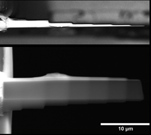
Physical data for this study were collected by creating thin lamellae of Al2O3 (Kyocera Global) and FeS2 (Alfa Aesar). Small pieces of each material were prepared on SEM stubs and loaded into an FEI Nova DualBeam focused ion beam (FIB) instrument to extract specimens for analysis. The lamellae were thinned to create multiple terraced segments within each sample with thicknesses varying between approximately 0.4 and 2 microns. These segments are distinguishable in the high-contrast top-down and cross-sectional backscatter electron images of each sample presented in Figure 2.

Figure 2: Top-down (upper) and cross-sectional (lower) high-contrast backscatter electron images of the FeS2 (left) and Al2O3 (right) samples used for EDS line scan experiments.
Target thicknesses for each segment were selected to span a range of absorption levels as predicted by Monte Carlo simulations. The actual approximate thicknesses were determined from top-down imaging of the specimens in a ThermoFisher Apreo LoVac field emission SEM, which was also used for all imaging and spectroscopy experiments.
EDS data were collected using an EDAX Octane Elect Plus 30 mm2 EDS detector and the TEAM software package. The collection scheme consisted of 20–25 μm line scans with 200 nm step sizes and 50 ns dwell times, with each line repeated 25 times. Beam current and detector settings were adjusted to obtain total raw peak intensities of order 100,000 or more per step for each element. This protocol was applied to each sample at 10, 15, 20, 25, and 30 kV. The raw data were analyzed within TEAM using four proprietary EDAX models, first the SEM “eZAF” standardless matrix correction algorithm for bulk specimens, and then multiple versions of the TEM “MThin” model designed for freestanding films. The MThin models were set up to account for absorption and material density using the default Zaluzec option, and then run assuming constant sample thicknesses of 0.5 μm, 0.75 μm, and 1 μm to establish general trends. More information about these models can be found in references [Reference Eggert17] and [Reference Sandborg18], respectively.
Results
Example results of simulated X-ray trajectories are provided in Figure 3 for fixed beam energy at different sample thicknesses, and in Figure 4 for different beam energies at fixed sample thickness. The top of each panel indicates the corresponding X-ray transition, accelerating voltage, sample thickness, and total area depicted.

Figure 3: Simulated K-edge X-ray volumes for fixed beam energy (30 keV) and variable sample thickness (0.5, 1, and 2 μm) illustrating conditions that resulted in absorption, semi-transparency, and transmission.

Figure 4: Simulated K-edge X-ray volumes for variable beam energy (10, 20, and 30 keV) and fixed sample thickness (1 μm) illustrating conditions that resulted in absorption, semi-transparency, and transmission.
Simulation results indicating ~0.5 to ~2 micron sample thicknesses should span the desired range of beam-sample interactions and transparency levels, from approaching TEM-like conditions at 30 kV and 0.5 micron thickness in Al2O3 (Figure 3), to nominally SEM-like behavior at 10 kV and 1 micron thickness in FeS2 (Figure 4). These results were examined to hypothesize if and when accurate composition analysis could be expected from application of the eZAF or MThin models mentioned earlier, as indicated in Tables 1 and 2.
Table 1: Summary indicating the conditions that either the eZAF or MThin data analysis approach was expected to produce accurate quantitative results for SEM-EDS experiments at different beam energies and sample thicknesses for freestanding Al2O3 thin films, as determined by examination of Monte Carlo simulations.

Table 2: Summary indicating the conditions that either the eZAF or MThin data analysis approaches were expected to produce accurate quantitative results for SEM-EDS experiments at different beam energies and sample thicknesses for freestanding FeS2 thin films, as determined by examination of Monte Carlo simulations.

Based on top-down imaging of each sample (Figure 2), the estimated segment thicknesses are: 0.505 μm, 0.885 μm, 1.00 μm, and 1.17 μm in Al2O3; and 0.457 μm, 0.523 μm, 0.809 μm, 0.893 μm, 1.204 μm, and 1.825 μm in FeS2.
To understand the results of the EDS line scans, we begin with Figure 5, which contains two components. The top panel shows the same top-down image of FeS2 from Figure 2 where the segments of different thickness are labeled, while the bottom panel contains a corresponding plot showing the normalized intensity of the S K edge as a function of position. As the beam scans across the sample into regions of different thickness, we see associated decreases in X-ray emission from one segment to another are seen. This change occurs because the relative fraction of X-ray volume contained within each segment decreases with increasing beam transmission, as expected.

Figure 5: Top-down backscatter electron image of FeS2 lamella (upper panel) registered to a plot showing normalized intensity of S K-L3 edge as a function of beam energy and scan position (lower panel). Upper and lower panels are spatially aligned to illustrate how the normalized intensity varies within and between different segments.
Extending this analysis approach further, Figure 6 shows normalized intensities of detected K-edge X-rays for all four elements in the two samples as a function of scan position. Similar variations in normalized intensity are observed as the beam scans across each segment, though the relative change from segment to segment is different for each element.

Figure 6: Normalized K edge intensities vs. line scan position for each of the labeled elements at the various beam energies used in this study.
There are two aspects of the data that warrant explanation. The unusual shape of the Al and O lines results from the presence of a grain boundary within the second segment of the Al2O3 sample (visible in Figure 2), which corresponds with a variation in sample density and thereby affects the trajectory of the beam and intensity of X-ray signal detected from this region. Also, the 10 kV data are omitted for Fe because the overvoltage was insufficient to provide useful results.
To emphasize the change in relative intensity of the X-ray signals for the individual elements in each compound, the ratio of the normalized intensities in Figure 6 are plotted as a function of scan position in Figure 7 (Al/O and S/Fe). Deviations from unity in Figure 7 indicate a thickness-dependent change in the ratio of detected intensity of the elements’ K-edge X-rays, corresponding with relative variations in X-ray volume, which confirms these conditions are well within the “semi-transparent” regime (middle panels of Figure 1). These thickness and energy-dependent variations must arise from differences in parameters such as ionization cross sections and mass absorption coefficients, pointing to areas for further study.

Figure 7: Ratio of normalized K edge X-ray intensities (Al/O and S/Fe) vs. line scan position for the two elements in each compound at the various beam energies used in this study.
Relative peak intensities are important because they are the basic input for EDS quantification algorithms, meaning we can expect dramatic corresponding differences in composition analysis from each semi-transparent segment, regardless of which model we apply.
Finally, Figure 8 shows the quantitative analysis results after running the original raw data through the four models described earlier. These results are presented as normalized Al and S content for each sample as a function of scan position; in this format, 1.0 is a “correct” match to the known composition. The light green shaded bar around 1.0 corresponds with a width of approximately ±0.02.
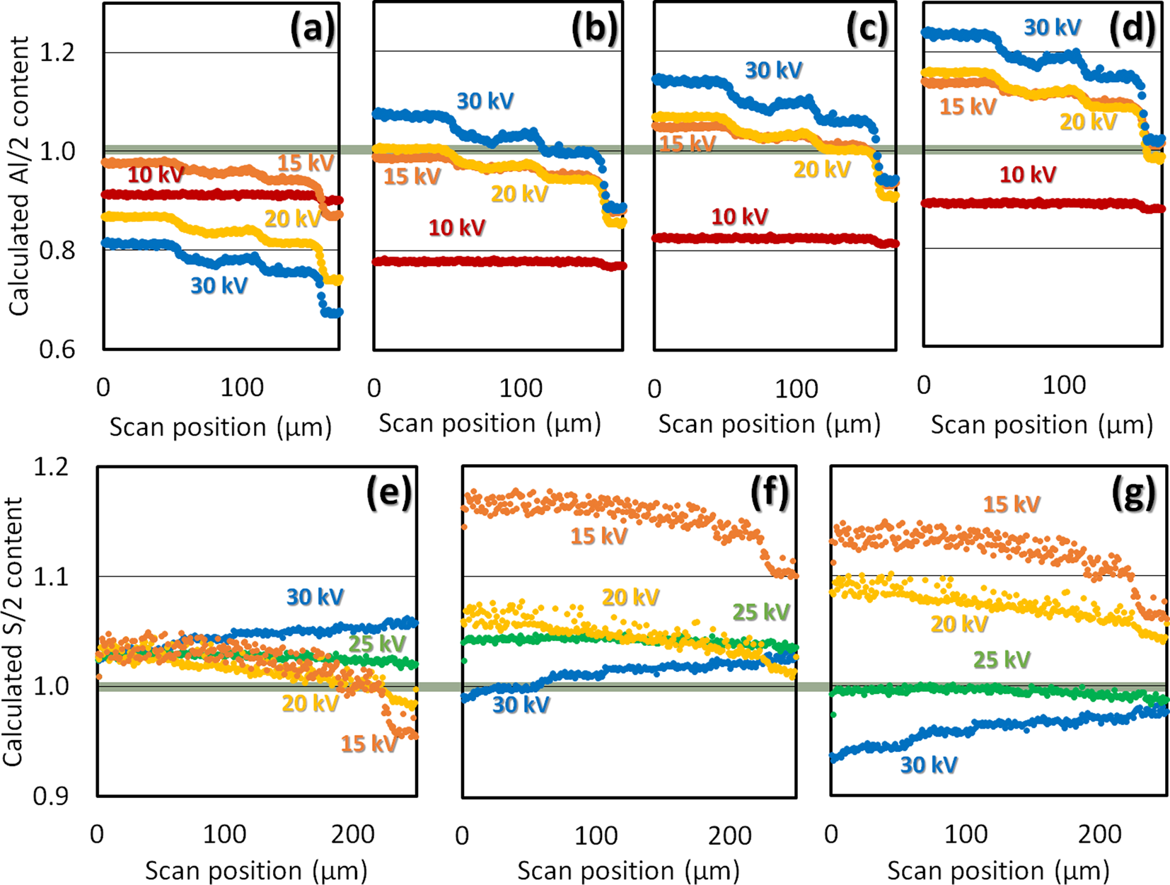
Figure 8: Quantification results for Al2O3 (a–d) and FeS2 (e–g), normalized to the expected Al or S content and plotted as a function of scan position. Panels (a) and (e) result from running the raw data through the conventional SEM “eZAF” algorithm, while the others show results from the TEM “MThin” model accounting for absorption and material density while assuming constant sample thicknesses of 1 μm (b), 0.75 μm (c, f), and 0.5 μm (d, g).
There are two notable omissions in Figure 8. First, the results for FeS2 analyzed with the “MThin 1 μm” model are excluded, as there are zero accurate results, and they provide no additional useful information; instead, they simply continue the trend of shifting the calculated S content to larger values, deviating further from the correct answer. Similarly, the results for Al2O3 analyzed at 25 kV are excluded, since (as seen in Figure 7) the data so closely resemble the results at 30 kV they are indistinguishable when plotted together.
Based on the data in Figure 8, Tables 3 and 4 summarize the combinations of material type, beam energy, sample thickness, and algorithm that produce accurate quantification results within ~2%.
Table 3: Summary of circumstances where the combination of Al2O3 sample thickness, beam energy, and quantification algorithm successfully reproduced the known composition of the material within 2% error.

Table 4: Summary of circumstances where the combination of FeS2 sample thickness, beam energy, and quantification algorithm successfully reproduced the known composition of the material within 2% error.

Discussion
First, regarding the raw data, the results for FeS2 are intriguing. As seen in Figure 7, the thickness-dependent ratio of Fe and S X-ray intensities inverts between 30 kV and 20 kV, with the data at 25 kV appearing to have essentially no thickness dependence. This reveals a crossover point where the factors affecting K-edge X-ray volume equate for Fe and S in FeS2, occurring coincidentally at the same voltages where beam transmission is maximized, and at the voltages most commonly used for SEM-EDS analysis. The ambiguity of if and when such a crossover in X-ray volume might occur emphasizes the challenge in establishing general guidelines for SEM-EDS analysis of freestanding films.
Second, we note many of the correct answers identified in Tables 3 and 4 are actually false positive errors where the model accurately identified the known material composition, but not intentionally. This happens whenever algorithm inputs (intensity ratios, etc.) coincide with expected behavior for the modeled circumstances, even if requisite assumptions are not satisfied (for example, full beam absorption). We also observe several nominally false negative errors where the composition was expected to be identified accurately but was not.
Third, we point to the only circumstances where the hypothesized outcomes were realized: the thinnest Al2O3 segment (~0.5 μm) produced accurate composition results using the MThin 0.5 μm model for all beam energies where substantial transmission occurred, while the next thinnest segment (~0.885 μm) was accurately analyzed with the MThin 1 μm model at 25 and 30 kV.
Explanations for these results—those that are accurate and erroneous—can likely be produced from a more complete knowledge of the quantification algorithms’ inner workings, and/or by considering the finer details of semi-transparency and EDS analysis in general, for example, the role of overvoltage, differences in background X-ray intensity, effects of reflected waves at the exit surface of thin specimens, etc. Examination of these points is left for future work.
Although 10 kV analysis was unsuccessful here, low kV EDS is still very much an attractive approach, especially since it does not require foreknowledge of the sample thickness or density. Since every element except H and He has at least one primary X-ray transition below 5 keV, low-energy EDS analysis is always possible, in principle, even when using incident beam energies below 10 keV [Reference Newbury and Ritchie15,Reference Marks16]. However, low overvoltage ratios mean element identification relies mainly on L and M edge X-rays, which are prone to re-absorption, are generally not detected efficiently, tend to overlap with each other, and have peak shapes that may be affected by bonding. These obstacles can be partially mitigated by high-quality hardware and software designed specifically for low-energy EDS analysis, such as windowless detectors and advanced peak deconvolution algorithms. In other words, a properly equipped and/or skilled operator should, in theory, be able to successfully apply the bulk absorption model to analyze EDS data collected at sufficiently low beam energies on otherwise semi-transparent samples. In the absence of such tools, however, this approach seems unlikely to be practical, even if it is successful.
That leaves us to consider the utility of the opposite extreme, embracing transmission and aiming to satisfy the “thin film” assumptions regarding X-ray absorption and secondary fluorescence. Successful application of this approach seems more likely on thinner samples (<0.5 μm) and if the operator has at least some knowledge of the sample thickness and composition in advance, which may not always be possible. SEMs are also not immune from artifacts present in TEMs, including spurious X-ray generation. However, using higher kV provides the benefits of more overvoltage and the excitation of more easily separated X-ray peaks at higher energy.
Conclusions
To provide insight into the most effective approach to quantitative SEM-EDS analysis of freestanding thin films, a systematic study of terraced Al2O3 and FeS2 lamellae, in conjunction with Monte Carlo simulations, is reported. While some accurate quantification results were acquired by applying a TEM model to data collected at high voltage on submicron-thick segments of Al2O3, most results from this study are erroneous. This illustrates how exceptionally easy it is to produce inaccurate SEM-EDS analysis of freestanding films, even under nominally (or naïvely) appropriate combinations of beam energy and sample thickness. Energy and thickness-dependent X-ray volumes become major hindrances to accurate analysis when incident electron beams are mostly, but not fully, absorbed by thin specimens.
While the present work leaves significant room for further study, we can at least say with confidence that attempting quantitative (or even qualitative) composition analysis of freestanding films in SEMs is treacherous ground at best. In the absence of analytical models designed specifically for semi-transparent materials, optimal results appear most likely to be obtained by turning the experiment into one that more closely resembles either conventional SEM or TEM conditions.
Which method is most appropriate depends on the capabilities of available hardware and software, the desired goals of the research, and the properties of the material under examination. In a system optimized for low kV EDS analysis, and with samples that are relatively thick (>0.5 μm), conventional bulk SEM analysis methods may be superior. Otherwise, without those tools, and/or when dealing with samples thinner than 0.5 μm, a TEM-like approach may be more reliable. Either way, it is strongly recommended that data be collected at a series of voltages to look for indications of semi-transparency affecting the results, since the correct result should, ideally, have no dependence on beam energy.
Acknowledgments
The author is grateful for the input and advice of Henk Colijn, Daniel Huber, Robert Williams, and Daniel Veghte. All sample preparation and electron microscopy was performed at the OSU Center for Electron Microscopy and Analysis.


