


Introduction
The size and orientation of grains in nanocrystalline materials are directly related to material properties (Meyers et al., Reference Meyers, Mishra and Benson2006). Therefore, the quantitative measurement of local crystallographic orientations is required to understand the structure–property relationship at nanometer scales. For this purpose, several transmission electron microscopy (TEM)-based methods (Schwarzer, Reference Schwarzer1997) have been developed, such as dark-field conical scanning (Li & Williams, Reference Li and Williams2003; Dingley, Reference Dingley2006; Wu & Zaefferer, Reference Wu and Zaefferer2009), convergent beam electron diffraction (Fundenberger et al., Reference Fundenberger, Morawiec, Bouzy and Lecomte2003), and nanobeam diffraction (NBD) in scanning transmission electron microscopy (STEM) (Ganesh et al., Reference Ganesh, Kawasaki, Zhou and Ferreira2010). Scanning precession electron diffraction (SPED) is also widely used in TEM because the acquisition of diffraction patterns and orientation indexing of each pattern can be carried out automatically which is suitable for automated crystal orientation mapping (Rauch et al., Reference Rauch, Véron, Portillo, Bultreys, Maniette and Nicolopoulos2008, Reference Rauch and Dupuy2010; Portillo et al., Reference Portillo, Rauch, Nicolopoulos, Gemmi and Bultreys2010; Viladot et al., Reference Viladot, Véron, Gemmi, Peiró, Portillo, Estradé, Mendoza, Llorca-Isern and Nicolopoulos2013; Cooper et al., Reference Cooper, Bernier and Rouvière2015). Diffraction patterns of individual crystallites are acquired by scanning a focused electron beam in a two-dimensional (2D) array on the sample and synchronized 2D diffraction patterns are recorded at each probe position, referred to as 4D-STEM (Ophus, Reference Ophus2019).
In SPED, the 4D-STEM method is extended by the precession of the ~1 nm-sized incident beam at a constant angle on a conical surface around the optic axis. By recording diffraction patterns with the incident electron beam in precession, the diffraction spot intensities are integrated with an angular range across different diffraction conditions. As a result, quasi-kinematical conditions are achieved by suppressing dynamical scattering effects and a wider range of reflections is excited, which greatly improves the quantitative interpretability of diffraction patterns (Vincent & Midgley, Reference Vincent and Midgley1994; Own et al., Reference Own, Sinkler and Marks2006; Oleynikov et al., Reference Oleynikov, Hovmöller and Zou2007; Portillo et al., Reference Portillo, Rauch, Nicolopoulos, Gemmi and Bultreys2010). An orientation map is reconstructed by indexing each diffraction pattern in the 4D-STEM dataset using a template matching algorithm (Rauch & Dupuy, Reference Rauch and Dupuy2005; Rauch et al., Reference Rauch, Portillo, Nicolopoulos, Bultreys, Rouvimov and Moeck2010). SPED enables phase identification and local crystallographic orientation determination of nanostructured or nanocrystalline materials with a high spatial resolution.
However, orientation indexing is often difficult when the acquired diffraction pattern contains all reflections from superimposed grains along the sample thickness (Kobler & Kübel, Reference Kobler and Kübel2017; Rauch & Véron, Reference Rauch and Véron2019). In addition, detailed features such as sub-grain boundaries are difficult to resolve with SPED because of the limited angular resolution (~1°) of the technique (Zaefferer, Reference Zaefferer2011; Morawiec et al., Reference Morawiec, Bouzy, Paul and Fundenberger2014). In scanning electron microscopy (SEM), transmission Kikuchi diffraction (TKD) has been used as an alternative method for the characterization of nanomaterials because it has the required spatial resolution and high angular resolution (Trimby et al., Reference Trimby, Cao, Chen, Han, Hemker, Lian, Liao, Rottmann, Samudrala, Sun, Wang, Wheeler and Cairney2014; Sneddon et al., Reference Sneddon, Trimby and Cairney2016; Liu et al., Reference Liu, Lozano-Perez, Wilkinson and Grovenor2019; Ernould et al., Reference Ernould, Beausir, Fundenberger, Taupin and Bouzy2020; Sugar et al., Reference Sugar, McKeown, Banga and Michael2020; Jeong et al., Reference Jeong, Jang, Kim, Kostka, Gu, Kim and Oh2021).
The conventional SPED system cannot utilize the orientation sensitive, weak, and small diffraction spots at high scattering angles due to the difficulty of capturing those reflections. In conventional SPED configurations, an external charge-coupled device (CCD) camera is used to capture diffraction patterns from a fluorescent screen during nanobeam scanning (Moeck et al., Reference Moeck, Rouvimov, Rauch, Véron, Kirmse, Häusler, Neumann, Bultreys, Maniette and Nicolopoulos2011). When the diffracted electrons collide with a fluorescent screen, a phosphor on the fluorescent screen is excited. This produces emitted visible light proportional to the electron intensities on the fluorescent screen. The external CCD camera captures this light as images with an off-axis geometry, which are passed through additional postprocessing steps, such as distortion and inclination corrections (Moeck et al., Reference Moeck, Rouvimov, Rauch, Véron, Kirmse, Häusler, Neumann, Bultreys, Maniette and Nicolopoulos2011; Eggeman et al., Reference Eggeman, Krakow and Midgley2015; Yao et al., Reference Yao, Amin-Ahmadi, Li, Cao, Ma, Zhang and Schryvers2016). Although the CCD camera has a high frame rate (~180 frames/s) and high sensitivity for fast mapping (Moeck et al., Reference Moeck, Rouvimov, Rauch, Véron, Kirmse, Häusler, Neumann, Bultreys, Maniette and Nicolopoulos2011), acquired patterns contain afterimages from the last several positions of the probe because the fluorescent screen continues to emit light ~100 ms after a diffraction spot has disappeared (Shionoya & Yen, Reference Shionoya and Yen1998). Due to the various electron to light and light to electron conversion steps in current data acquisition systems, the signal-to-noise ratio for this technique is suboptimal. Hence, this conventional SPED configuration suffers from limitations that introduce scanning artifacts, obscure the detection of weak reflections and strongly restrict the angular resolution of this spot-based technique in the TEM.
Although there is a detrimental effect due to the suboptimal configuration of the conventional system, in-built detector configurations consisting of a CCD sensor with a phosphor and fiber-optic coupling were not widely used due to limited dynamic range and slow-scan speed in the past (Fan & Ellisman, Reference Fan and Ellisman1993). The phosphor (and fiber-optic), which converts the signal from a high-energy incident electron into a pulse of light photons, was an essential component because the CCD sensor is easily damaged by direct illumination of the focused electron beam. In TEM, recent advances have focused on the development of direct electron detectors in which incident electrons directly create electron–hole pairs and then read out in a semiconductor (Clough et al., Reference Clough, Moldovan and Kirkland2014; McMullan et al., Reference McMullan, Faruqi and Henderson2016). High dynamic range, high electron sensitivity, and readout speed of those detectors have propelled their application in numerous 4D-STEM applications (Ophus, Reference Ophus2019). One type of direct electron detectors is a hybrid pixel array detector (PAD) which can be used for capturing high-intensity reflections with a high dynamic range (Yang et al., Reference Yang, Jones, Ryll, Simson, Soltau, Kondo, Sagawa, Banba, MacLaren and Nellist2015; Mir et al., Reference Mir, Clough, MacInnes, Gough, Plackett, Shipsey, Sawada, MacLaren, Ballabriga, Maneuski, O'Shea, McGrouther and Kirkland2017a; Nord et al., Reference Nord, Webster, Paton, McVitie, McGrouther, MacLaren and Paterson2020). A diffraction pattern is recorded as an image with a low number of pixels (Normally 256 × 256 pixels) with a large pixel pitch in favor of high electron sensitivity. Recently, MacLaren et al. showed an improvement in phase and orientation indexing reliability using diffraction patterns acquired by a hybrid PAD (MacLaren et al., Reference MacLaren, Frutos-Myro, McGrouther, McFadzean, Weiss, Cosart, Portillo, Robins, Nicolopoulos, Nebot del Busto and Skogeby2020). Another type of detector is complementary metal-oxide-semiconductor (CMOS) based on monolithic active pixel sensors (APS). This CMOS with APS allows bigger arrays (16, 24, or 64 megapixels), faster readout, reduced noise, and reduced sensitivity to radiation damage compared with CCD (Ghadimi et al., Reference Ghadimi, Daberkow, Kofler, Sparlinek and Tietz2011; Bammes et al., Reference Bammes, Rochat, Jakana, Chen and Chiu2012; Contarato et al., Reference Contarato, Denes, Doering, Joseph and Krieger2012). However, this type of detector has limited applicability for capturing NBD patterns including the high intensity transmitted beam because the detector can be damaged by high electron dose due to the very thin electron-sensitive volume. This drawback can be overcome by using a scintillator-coupled CMOS detector. Although electron sensitivity can be slightly degraded due to the configuration of indirect electron detection, the dynamic range and capacity of high electron dose can be adapted by optimizing the scintillator (Rodriguez & Gonen, Reference Rodriguez and Gonen2016). However, orientation mapping using a scintillator-coupled CMOS detector has not been thoroughly investigated or discussed yet.
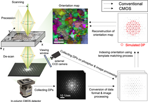
In this study, we demonstrate orientation mapping with precession electron diffraction (PED)-assisted 4D-STEM using a scintillator-coupled CMOS detector in TEM. In each nanobeam probe position, a high-quality diffraction pattern is acquired with a simultaneous precession of the electron nanobeam. The scintillator was found to be robust during measurement in a TEM operating at 200 kV. Considering the widespread use of the conventional SPED system in nanoscale orientation analysis, we first compared two systems (i.e. the conventional system and a scintillator coupled CMOS detector) by collecting 4D-STEM datasets in the same area of a sample. The data are compared in terms of the quality of the diffraction patterns and orientation maps. The following section focuses on the CMOS system with the optimization of the template matching process to improve the angular resolution of diffraction spot patterns.
Experimental Procedures
TEM Sample Preparation
For quantitative measurement of diffraction pattern images, a thin lamella of single-crystal Si was prepared in a Scios 2 focused ion beam (FIB, ThermoFisher). The acceleration voltage of the Ga+ ion beam during FIB milling was 30 kV. To minimize the surface damage layers, a final low-energy cleaning step was performed at 0.5 kV.
For orientation mapping, a thin foil of nanocrystalline Cu–Ag alloy with a thickness of 5 μm was used (Oellers et al., Reference Oellers, Arigela, Kirchlechner, Dehm and Ludwig2020). A disc with a diameter of 3 mm was cut out from the foil using a disc puncher and glued to a Cu single hole grid. For perforation, Ar+ ion milling was performed at 2.5 kV using a PIPS II system (Gatan). Low-energy milling was followed at 0.5 kV to minimize the surface damage and to extend the electron transparent area.
PED-Assisted 4D-STEM Data Acquisition
PED was performed in a JEM-2200FS TEM (JEOL) operating at 200 kV and equipped with ASTAR (Nanomegas). The microscope was operated in NBD mode with the smallest spot size and a condenser aperture size of 10 μm. The probe size was measured as ~ 1 nm in diameter with a convergence angle of 2 mrad. A precession frequency of 100 Hz and a precession angle of 0.5° were applied during the nanobeam scanning.
The overall procedure of the orientation mapping using the conventional configuration and the in-column CMOS system are summarized in Figure 1, respectively. To compare the data quality between the conventional and CMOS camera systems, PED patterns and datasets were acquired in the same region on the same specimen. The first dataset was acquired using the conventional off-axis system filming the fluorescent screen with a Stingray CCD camera (NanoMegas) (labeled as “Conventional” in Fig. 1). This setup is referred to as the conventional configuration in the remainder of the paper. Each acquired pattern has 144 × 144 pixels with an 8-bit depth. The scan size was 150 × 75 pixels with a step size of 2 nm, yielding a scanning area of 300 × 150 nm2. The second dataset was recorded using an on-axis TemCam-XF416 pixelated CMOS detector (TVIPS) (labeled as “CMOS” in Fig. 1). The Universal scan generator (TVIPS) was used for synchronizing the scanning with the acquisition of diffraction patterns. The step size was ~2.7 nm for the same scanning area of 300 × 150 nm2. The diffraction patterns had a pixel size of 2k × 2k (2× hardware binning of the full 4k detector area) with 16-bit depth. The exposure time for the acquisition of each diffraction pattern was chosen as 50 ms in both experiments by considering the persistent time of the fluorescent screen (~100 ms) in the conventional system. It might be helpful to reduce the effect of afterimage in each acquired pattern compared to shorter exposure times. A camera length of 15 cm was selected for all diffraction patterns.
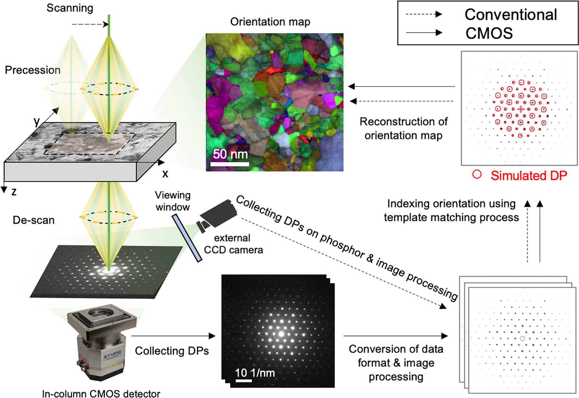
Fig. 1. Overview of PED orientation mapping analysis using conventional and CMOS camera systems used in the present study.
Data Processing and Orientation Indexing
Orientation indexing of both conventional and CMOS datasets was performed by template matching (Rauch et al., Reference Rauch, Portillo, Nicolopoulos, Bultreys, Rouvimov and Moeck2010) using the ASTAR software package. Note that all images of the CMOS dataset were binned to 512 × 512 pixels (binning factor of 4) or 128 × 128 pixels (binning factor of 16) and converted to 8-bit depth using a custom-written Python package (Cautaerts, Reference Cautaerts2020) because the ASTAR software cannot handle the large CMOS dataset nor 16-bit data. The result of this conversion is shown in Supplementary Figure S1. By increasing the binning factor and decreasing bit depth, the diffraction pattern gets more pixelated and the number of gray scale values decreased from 1-65535 to 1-255 (Supplementary Fig. S1). Before template matching was performed, there were default settings for image processing with six different functions (i.e. softening loops, spot enhance loops, spot detection radius, noise threshold, gamma correction, and polar image max work radius). Since artifacts can be induced at some stage, we carefully adjusted these parameters, especially, softening loops, spot enhance loops, and spot detection radius.
The matching index (Q) and reliability (R) of orientation indexing were calculated during the template matching process (Rauch & Dupuy, Reference Rauch and Dupuy2005; Rauch & Véron, Reference Rauch and Véron2014). A library of diffraction templates was generated with a lattice parameter of a = 3.615 Å for Cu. In the template matching process, experimental patterns are compared to every simulated template that is computed for all possible crystal orientations of all expected phases (Rauch & Dupuy, Reference Rauch and Dupuy2005). The orientation of each experimental pattern is determined to that of the specific simulated template which has the highest matching index. The matching index is determined by a cross-correlation between an experimental pattern and a simulated pattern as given by the following equation.
 $$Q = \displaystyle{{\mathop \sum \nolimits_{\,j = 1}^m P( {x_j, \;y_j} ) T_i( {x_j, \;y_j, \;\phi_1} ) } \over {\sqrt {\mathop \sum \nolimits_{\,j = 1}^m P^2( {x_j, \;y_j} ) } \sqrt {\mathop \sum \nolimits_{\,j = 1}^m T_i^2 ( {x_j, \;y_j, \;\phi_1} ) } }}$$
 A pattern is represented by the intensity function P(x, y) where x and y are the width and height of the image. For each individual template T i(x, y, ϕ 1) corresponding to a rotation ϕ 1 of the template i taken among the N families stored in the template database ( $\phi _1\in { {1^\circ , \;360^\circ } } , \;\;i\in { {1, \;N} }$), the summation is performed for every pixel in the pattern image (j ∈ {1, m}. Since the simulated pattern has only a limited number of non-zero datapoints (discrete position and intensity of reflections), typically only 50–100 products (i.e. the number of matching reflections) are added during the calculation.
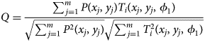
The reliability (R) of orientation indexing is calculated by a ratio of the two highest local maxima after the matching indexes were calculated as given by the following equation.
 $$R = 100\left({1-\displaystyle{{Q_2} \over {Q_1}}} \right)$$
where Q 1 and Q 2 are the two highest values of the matching indexes for distinct local maxima in all possible orientations.
After orientation indexing, the orientation data were exported (.ang format) and analyzed with the TSL-OIM software (EDAX Inc.). No clean-up process like grain dilation or grain neighboring process was performed to allow direct comparison.
Results
Direct Comparison of Diffraction Patterns Acquired by the Conventional and CMOS Systems
Figure 2 shows a direct comparison of diffraction patterns obtained by using the two different detector setups. Diffraction patterns were acquired near the [110] zone axis of single-crystal Si at the same location of the specimen. In the conventional configuration, the original diffraction pattern is stretched along the vertical axis since the fluorescent screen, where the pattern is acquired using the CCD camera, is inclined with respect to the image plane. After correcting for this inclination, a contraction of the pattern is observed (Fig. 2a). In the CMOS image, more reflections are captured due to the large acceptance angle of the CMOS detector at the same camera length (Fig. 2b). Distortions in the diffraction pattern acquired using the CMOS detector are mainly stemming from astigmatism and aberrations in the objective and projection lens system. The different magnification of the diffraction pattern can be easily adjusted by changing the camera length in diffraction mode.
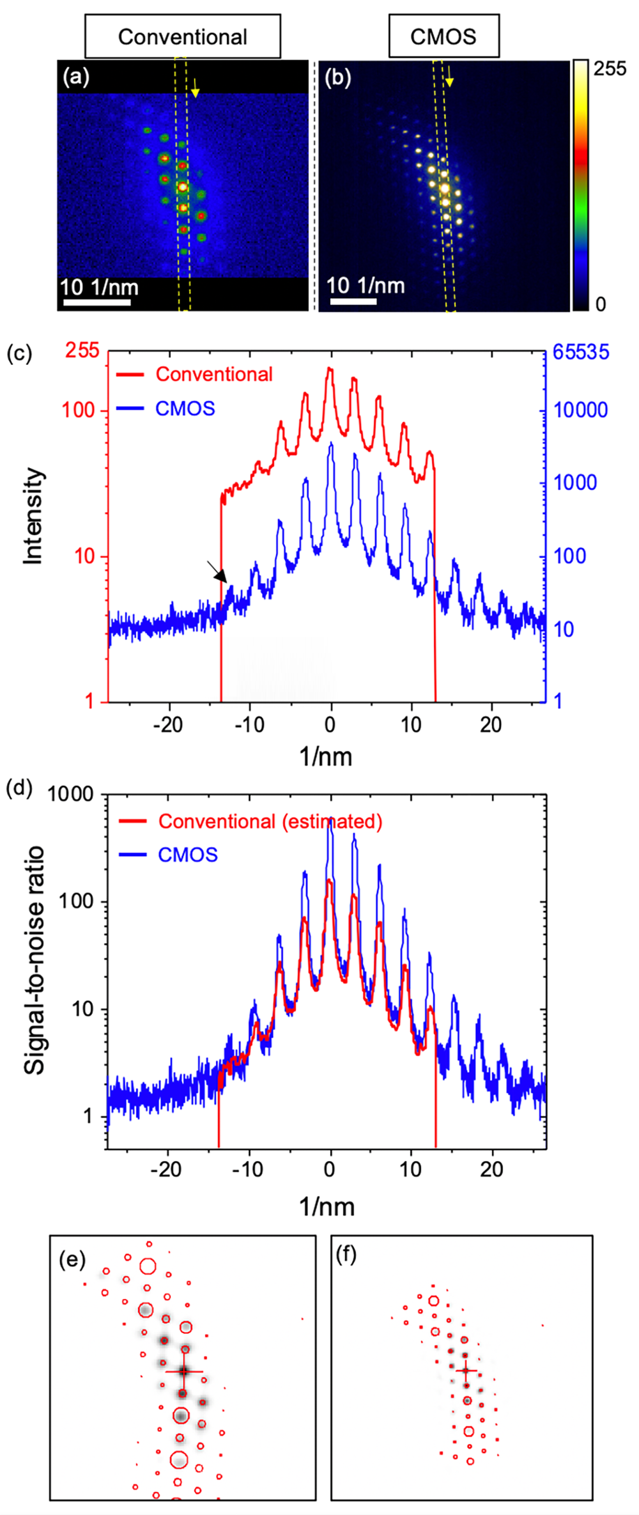
Fig. 2. Direct comparison of diffraction patterns showing near [110] zone axis of single-crystal Si obtained by using conventional and CMOS systems. Raw pattern images with temperature-color scale: (a) conventional (144 × 144 pixels) and (b) CMOS detector (2k × 2k pixels). Note that pixels with an intensity above 255 are shown as white color. (c) Intensity profiles and (d) signal-to-noise ratio measured along the same direction in the PED pattern images (marked as yellow square in a and b). Orientation indexing by template matching process for the pattern images obtained by (e) conventional and (f) CMOS detector. Diffraction spots displayed as red circles represent the simulated pattern with the highest matching index. The size of circles is indicating the relative radius of each reflection in the matched simulated pattern.
A quantitative comparison of intensity profiles extracted along 13 systematic row reflections of two representative nanobeam electron diffraction patterns is shown in Figure 2c. Due to the different magnification of pattern images (Figs. 2a, 2b), only eight reflections could be compared (indicated by vertical red lines for the conventional case in Fig. 2c). Note that the intensity of all pixels of the diffraction patterns is amplified with an exponent (~0.5) using a gamma correction of the conventional dataset. This function is normally used to compensate the limited dynamic range and the loss of signal during the data acquisition of the conventional system. This results in a shift of intensity levels from the lower to the middle range of intensities for the conventional dataset (Fig. 2c). Since the effective resolution of the diffraction spots in the conventional setup is largely determined by the point spread function of the phosphor screen, the relative intensities of the transmitted beam and a weak diffracted beam are not remarkable compared to the CMOS detector. In contrast, the pattern acquired by the CMOS detector shows a weak reflection at a high scattering angle (black arrow in Fig. 2c), which is resolved due to the high dynamic range. This result shows the CMOS detector can capture more weak reflections without exposing the camera to a point whereby the transmitted beam is saturated. The radial distribution of the background intensity is observed in both systems, which is mainly dominated by inelastically scattered electrons (Figs. 2a, 2b).
Since we used the gamma correction during the acquisition of conventional dataset, the direct comparison of signal-to-noise ratio between two systems is inappropriate because the gamma correction affects the measurement of signal-to-noise ratio. To estimate the signal-to-noise ratio of the conventional system without gamma correction, we calculated the signal-to-noise ratio by using a gamma exponent value of 0.5. The signal-to-noise ratio was calculated as the ratio between the measured intensity and the average intensity of dark noise measured by the conventional (Supplementary Fig. S2) and the CMOS detector (Supplementary Fig. S3). The average intensity of dark noise was measured as 18.96 for the external CCD with a gamma correction in conventional configuration and 6.07 for the CMOS detector (Supplementary Fig. S3b), respectively. The effect of gamma correction on signal-to-noise ratio is shown in Supplementary Figure S4. The signal-to-noise ratio for the CMOS detector is also up to ~5 times higher than that for the conventional system (Fig. 2d). The signal-to-noise ratio of the conventional configuration is degraded by the conversion efficiency of signal from diffracted electron to light on the fluorescent screen and the detection of reflected light through the viewing window with the external CCD camera (Fig. 1) during data acquisition. While there is a significant difference in image quality between the two methods, orientation determination by template matching is usually successful when the pattern image contains many reflections (e.g., zone axis) in both cases (Figs. 2e, 2f).
Direct Comparison of Orientation Maps Acquired by Conventional and CMOS Systems
The orientation maps of the nanocrystalline Cu–Ag alloy acquired by both systems from identical locations of the TEM sample are compared side-by-side in Figure 3. Note that orientation maps are reconstructed by template matching process using similar image resolutions of diffraction patterns [i.e. 144 × 144 pixels for conventional dataset and 128 × 128 pixels (binning factor ×16) for CMOS dataset (Supplementary Fig. S1c)] for fair comparison. The bright-field (BF) image (Fig. 3a) and matching index maps (Figs. 3b, 3c) show nano-sized grains with nanotwins. Σ3 twin boundaries and grain boundaries are represented as yellow (twin), black (high-angle grain boundary, misorientation angle >15°), green (low-angle grain boundary, 5° ~ 15° misorientation angle) on the orientation maps (Figs. 3d, 3e). The BF image (Fig. 3a) and raw orientation maps (Figs. 3b–3e) are broadly in agreement. However, fine details such as small grains (white arrow in Fig. 3e) and nanotwins (yellow arrow in Fig. 3e) can be detected only in the CMOS dataset. Kernel average misorientation (KAM) maps (Figs. 3f, 3g) show local misorientation within each grain to visualize sub-grain boundary (<5° misorientation). The KAM calculates the average misorientation between a pixel and its neighbors, provided that the misorientation does not exceed a predefined threshold value (here 5°). All KAM maps presented in this study were calculated with a fixed kernel to the third neighbors (default value). Sub-grain boundaries are not well shown in both orientation maps due to the limited orientation resolution. However, more artifacts within the grain are observed in the dataset obtained by the conventional configuration (Figs. 3d, 3f). Both methods show a reasonable reliability map (Figs. 3h, 3i) with some dark areas indicating low reliability due to grain overlapping. The orientation resolution is limited to ~1° (the maximum angular difference between adjacent templates is approximately 1° for a library with 1,326 templates) because orientations within 1° of all acquired patterns are only matched by one specific simulated pattern.
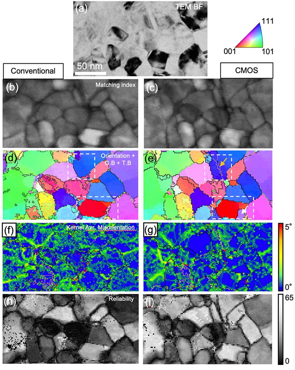
Fig. 3. Side-by-side comparison of orientation maps of nanocrystalline Cu–Ag sample acquired by conventional configuration and CMOS detector. (a) BF image, (b,c) matching index maps, and (d,e) orientation maps. Σ3 twin boundary and grain boundaries are represented as yellow (twin), black (high-angle grain boundary, misorientation angle >15°), green (low-angle grain boundary, 5° ~ 15° misorientation angle). (f,g) Kernel average misorientation maps. Sub-grain boundaries (0° ~ 5° misorientation angle) are displayed as a color scale. (h,i) reliability maps. The step size was 2 nm for conventional and ~2.7 nm for CMOS. Image resolutions of diffraction patterns were 144 × 144 pixels for conventional dataset and 128 × 128 pixels (binning factor ×16) for CMOS dataset. 1,326 simulated patterns (the maximum angular difference between adjacent templates is approximately 1°) were used for the template matching process.
A detailed comparison of the grain morphology and corresponding pattern indexing of the conventional and CMOS datasets acquired at the same sample regions are shown in Figures 4 and 5, respectively. Both figures show a BF image of the scanned region, the magnified orientation maps (white dotted square in Figs. 3d, 3e), and corresponding diffraction patterns. In the conventional case, the grain morphology in the orientation map of Figure 4b appears elongated along the scanning direction (i.e. left to right) when compared to the BF image shown in Figure 4a. The diffraction pattern acquired at this grain (marked as a blue circle in Fig. 4b) is matched well with the simulated pattern as shown in Figure 4d. However, when the beam scans the adjacent grain (marked as a yellow circle in Fig. 4b), the afterimage from the previous beam positions is partially present (white dotted circles in Fig. 4e) in the diffraction pattern of the adjacent grain. This effect is prominent in the reliability map because overlapping of afterimage and pattern image decreases the reliability (Fig. 4c). As a result, an incorrect orientation is obtained. This problem is notably observed when the beam is scanning from grains close to zone-axis orientation to grains oriented away from the zone axis or from the sample to vacuum (Viladot et al., Reference Viladot, Véron, Gemmi, Peiró, Portillo, Estradé, Mendoza, Llorca-Isern and Nicolopoulos2013). In the present study, the afterimage was observed along the scanning direction with a maximum of 10 pixels (20 nm with a step size of 2 nm), which results in a higher fraction of mis-indexed data points and a decrease in orientation reliability of the orientation map. By considering an exposure time of 50 ms, the persistence time of the afterimage on the fluorescence screen was estimated to be ~500 ms. The decay time might depend on the remaining lifetime of the fluorescent screen. In the CMOS maps, two nearby grains are distinguished (Figs. 4f, 4g) because there is no afterimage present in the diffraction pattern (Figs. 4h, 4i).
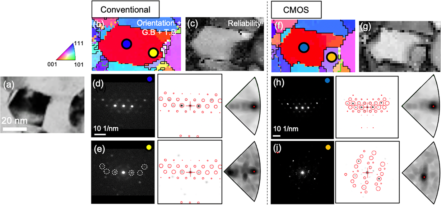
Fig. 4. Comparison of magnified orientation maps showing nano-sized grains acquired by conventional (Fig. 3d) and CMOS detector (Fig. 3e). (a) BF image. (b,f) magnified orientation maps. (c,g) reliability maps. (d,h) orientation indexing of the zone-axis oriented grain (marked as a blue circle in b and f). (e,i) orientation indexing of the adjacent grain (marked as a yellow circle in b and an orange circle in f). Reflections from after image are shown as white dot circles.
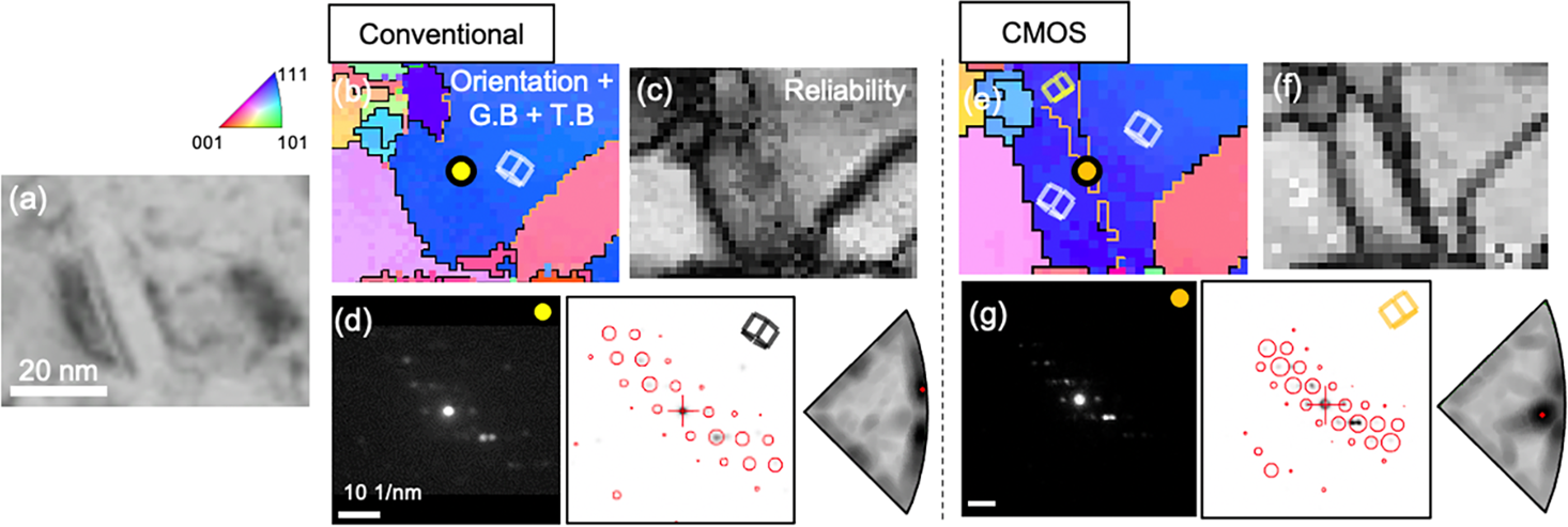
Fig. 5. Comparison of magnified orientation maps showing the grain containing nanotwin acquired by conventional system (Fig. 3d) and CMOS detector (Fig. 3e). (a) BF image. (b,e) Magnified orientation maps. (c,f) Reliability maps. (d,g) Orientation indexing of the nanotwin (marked as a yellow circle in b and an orange circle in e).
Figure 5 shows the orientation mapping analysis for a grain containing a nanotwin with a thickness of ~ 10 nm (Fig. 5a). In the case of conventional data, the nanotwin is not resolved in the orientation map (Fig. 5b) while it is diffusely observed in the reliability map (Fig. 5c). This is because the intensity of reflections in the matrix is amplified due to the afterimage formation in the conventional case as shown in Figure 4. This nanotwin is shown with a thickness of 1~2 pixels in the CMOS orientation map (Fig. 5e). However, the reliability is very low (Fig. 5f) because the diffraction patterns of the matrix and the twin are overlapping with similar intensity (Fig. 5g). Moreover, only a few reflections are visible since the beam direction is away from the zone-axis condition. Due to the advantage of the high dynamic range of the CMOS detector, this nanotwin could be observed by the recognition of a slight difference in the pattern intensity between matrix and twin (Fig. 5g). However, the morphology of the nanotwin is different from that observed in BF image (Fig. 5a). In addition, it is also difficult to verify whether this nanotwin is dominant or not (Fig. 5f).
Orientation Maps Acquired by the CMOS System with Improved Template Matching Process
Although weak reflections were captured by the CMOS detector, the default template matching algorithm cannot utilize weak reflections at high scattering angles. One example is shown in Figure 6. Weak reflections near the detector edge were not matched with the simulated pattern because the reflections near the transmitted beam dominate in the calculation of the matching index. Since they are not orientation sensitive, the template matching is unreliable with ambiguities (Fig. 6c) despite the presence of weak reflections (black arrows in Fig. 6b). In addition, only 1,326 templates could be used for orientation indexing because this problem is more pronounced when a larger number of templates were used (Rauch & Véron, Reference Rauch and Véron2014). This makes it difficult to resolve the fine details like sub-grain boundaries because the orientation resolution is limited to 1°.
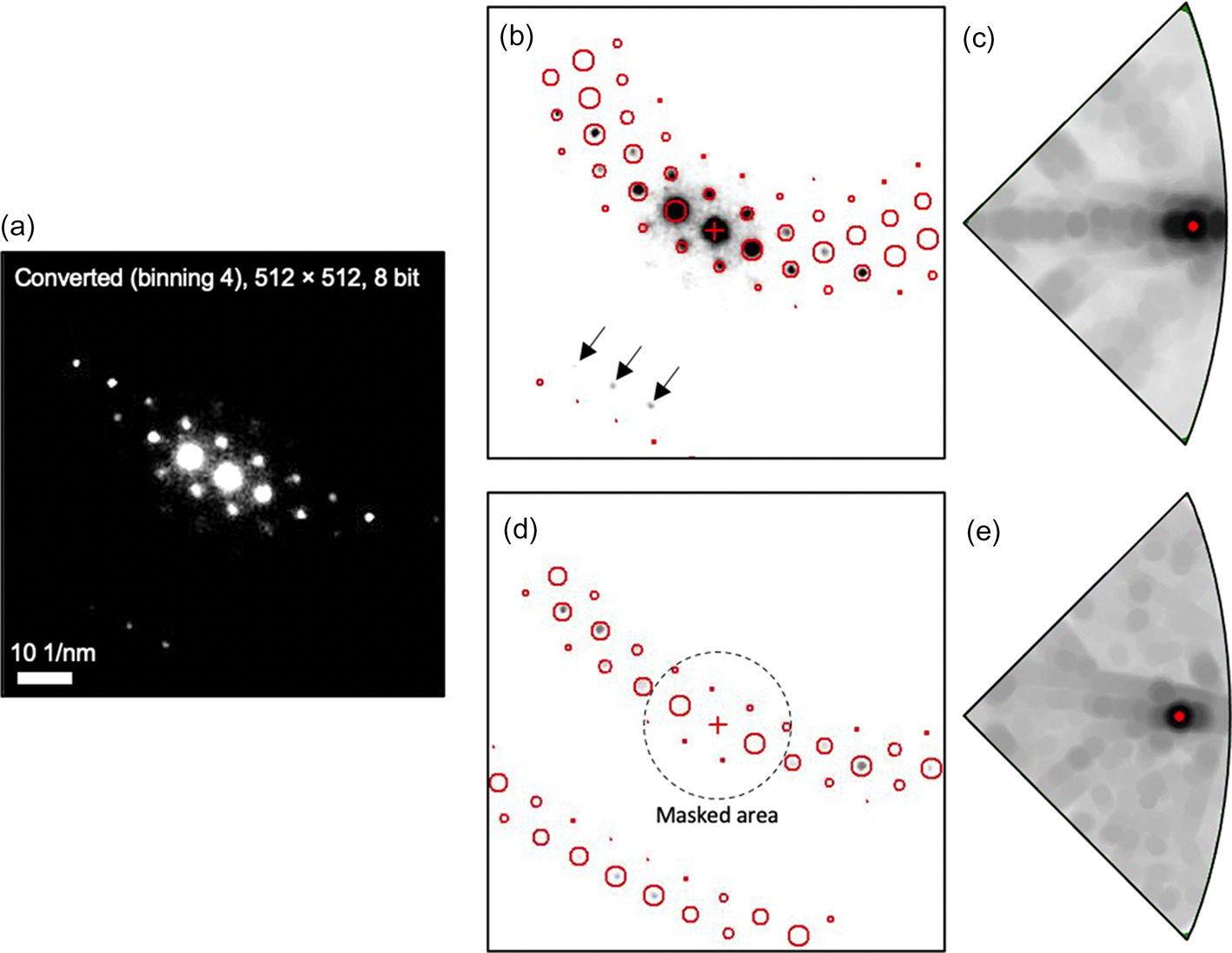
Fig. 6. Orientation indexing by template matching process for (a) the pattern image [512 × 512 pixels (binning factor × 4)] acquired by CMOS detector (b,c) without masking and (d,e) with masking of reflections near transmitted beam (<26 mrad). The masked area is displayed as a black dotted circle. Diffraction spots displayed as red circles represent the simulated pattern with the highest matching index. Orientation is indicated as a red dot in each index map (c,e). 11,476 simulated patterns were used for orientation indexing.
In order to solve this problem, we excluded reflections near the transmitted beam (dotted circle in Fig. 6d) in the experimental patterns using the fuzzy mask procedure as implemented in the ASTAR software package. The fuzzy mask applies a sigmoidal intensity cutoff of a selected area (here the central beam) in the image of an experimental diffraction pattern. As a result, only weak and small reflections at high scattering angles (>26 mrad) were considered for the template matching process. Even from a visual inspection, a better match of the experimental and simulated patterns is obtained (Fig. 6d). As those reflections are highly orientation sensitive, the reliability of this matching was significantly improved from 8 to 25 with a unique solution (Fig. 6e) while the matching index is decreased from 721 to 305 because the contribution of reflections near the transmitted beam was removed. Note that 11,476 simulated patterns were used for orientation indexing with a maximum angular difference between adjacent templates of approximately 0.33°.
The orientation maps of nanocrystalline Cu-Ag alloy acquired by the CMOS detector using the improved template matching process are shown in Figure 7. Compared to the orientation map reconstructed with conventional template matching (Figs. 3c, 3e), the number of artifacts was significantly reduced (Fig. 7b), especially for the detection of grain boundaries with 2° ~ 5° misorientation angle. Sub-grain boundaries within the grain are resolved in the KAM map (Fig. 7c). The reliability map (Fig. 7d) contains pixels with low reliability (low value), especially along the grain boundaries. The main reason why the reliability value decreases in the region of the nanotwin is that more than one possible solution from the overlapping patterns exists (Rauch & Véron, Reference Rauch and Véron2019). Note that every pixel can show only a single solution (orientation) with the highest value of matching index in the orientation map while two possible solutions are considered when reliability is calculated. In the reliability map, there are some pixels with low reliability inside the grain because the calculation of reliability was incorrect due to the difficulty of finding the two highest local maxima (first and second possible solution for orientation determination) in the matching index map when a large number of simulated patterns were used. Although the calculation of the reliability should be optimized further, these results show that the improved template matching process can significantly enhance the angular resolution of spot patterns when orientation sensitive and weak reflections at high scattering angles are detected in the experimental pattern. The precision and accuracy for the misorientation measurement were estimated using orientations of matrix and twin along the Σ3 twin boundary (white arrow in Fig. 7b) which was not resolved with the conventional case (Fig. 3b). Misorientation angles between matrix and twin were measured along the twin boundaries. Euler angles representing the orientation of the matrix and twin are shown in the supplementary material (Supplementary Table S1). The precision was calculated as the standard deviation of misorientations between matrix and twin. The accuracy was estimated by calculating the difference between ideal misorientation for Σ3 twin (60°) and average measured misorientation between matrix and twin. The angular resolution for misorientation measurement was estimated as 0.20° for precision and 0.27° for accuracy, which is comparable to that of Kikuchi lines (~0.3°) in TEM (Morawiec et al., Reference Morawiec, Bouzy, Paul and Fundenberger2014).
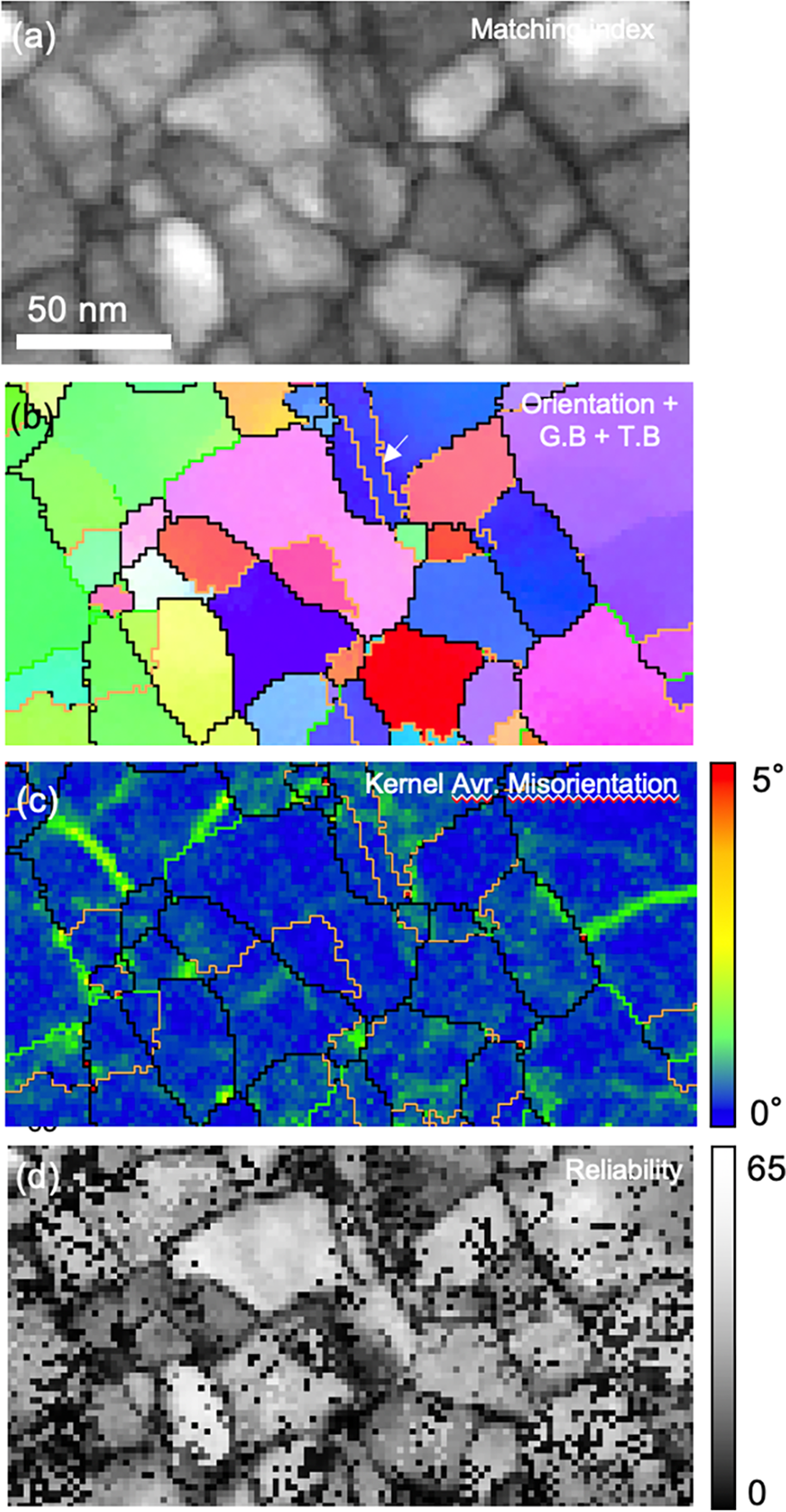
Fig. 7. Orientation maps of nanocrystalline Cu–Ag sample acquired by CMOS detector using improved template matching process (Fig. 6d). (a) Matching index map and (b) orientation map with Σ3 twin boundary and grain boundaries represented as yellow (twin), black (high-angle grain boundary, misorientation angle >15°), Green (low-angle grain boundary, 5° ~ 15° misorientation angle), and red lines (grain boundary, 2° ~ 5° misorientation angle). (c) Kernel average misorientation map. Sub-grain boundaries (0° ~ 5° misorientation angle) are displayed as a color scale. (d) Reliability map. Image resolution of diffraction patterns in 4D-STEM dataset was 512 × 512 pixels (binning factor × 4). 11,476 simulated patterns (the maximum angular difference between adjacent templates is approximately 0.33°) were used for the improved template matching process (Fig. 6).
Discussion
Improving the Template Matching Process & Angular Resolution of the Spot Pattern
In the template matching algorithm (Rauch & Dupuy, Reference Rauch and Dupuy2005), simulated patterns contain only position (not radius) and intensity information of each reflection. The correlation between experimental patterns in the 4D-STEM dataset and the simulated patterns in the template library is performed by calculating the matching index which is the sum of products (i.e. the discrete peak intensity values in the simulated pattern times the corresponding measured intensities in the experimental pattern). In simulated patterns, the intensity of reflections at a high scattering angle is relatively high because the atomic scattering factor is not considered (Rauch & Dupuy, Reference Rauch and Dupuy2005) when the pattern was generated, while the intensity of reflections gradually decreases depending on the scattering angle in the experimental pattern (Fig. 2c). This increases the contribution of weak reflections when the matching index is calculated.
However, the current template matching process still could not fully utilize those reflections (Fig. 6b) because orientation indexing is dominated by the high-intensity reflections near the transmitted beam. As these reflections are still close to dynamical diffraction condition under PED and their intensity contains contributions from inelastically scattered electrons, this gives them outsized weight in the calculation of matching index regardless of the contribution of weak reflections. In addition, since they are not orientation sensitive, it can induce mis-indexing of orientation unless the experimental pattern is perfectly corrected in pixels. Therefore, we optimized the template matching process to avoid mis-indexing by applying a fuzzy mask to exclude the reflections near the transmitted beam when the matching index is calculated. As only orientation sensitive and weak reflections are considered, this results in a better agreement between two patterns with an increase of reliability but a decrease in the absolute value of the matching index (Fig. 6).
Orientation mapping with spot patterns in TEM has been shown to have reduced angular resolution compared to Kikuchi-based analysis (Zaefferer, Reference Zaefferer2011; Morawiec et al., Reference Morawiec, Bouzy, Paul and Fundenberger2014). However, the angular resolution of spot patterns in TEM was not optimized because the conventional data acquisition system has a limited acceptance angle, limited dynamic range, the low resolution of the diffraction images, and low signal-to-noise ratio for detecting weak reflections at high scattering angles. Moreover, although those reflections were captured by the CMOS detector, the current template matching process still has a suboptimal angular resolution. With masked patterns, we could achieve more accurate orientation maps utilizing a large number of templates (high orientation resolution) (Fig. 7).
With the optimization of the acquisition system, number of templates, image resolution of experimental patterns, and image processing, detailed features are getting resolved in the orientation map. One example is the morphology of a nanotwin (Supplementary Fig. S5). The morphology of a nanotwin is gradually changed (Supplementary Figs. S5b, 5c) and finally matched with that of the BF image (Supplementary Fig. S5d). In addition, the reliability of resolving the nanotwin is significantly improved because intensity differences between the matrix and the twin can be clearly distinguished if we consider only reflections at high scattering angles. This indicates that the orientation sensitive, weak, and small diffraction spots at high scattering angles are most significant for orientation mapping.
The Performance of Detectors & Future Remarks
Since orientation mapping is directly affected by the raw image quality of the diffraction pattern, the performance of detectors and data acquisition process are important to obtain high-quality orientation maps. Table 1 shows a comparison between the external CCD camera and recently developed detectors: the scintillator-based CMOS detector and the reverse biased hybrid silicon diode PAD. Note that we only compared detectors which have been used for orientation mapping with SPED. Compared to the conventional case, CMOS and PAD have the advantage of being able to acquire high-quality diffraction images due to increased image resolution and higher dynamic range. Moreover, postprocessing of data is much less affected by artifacts because a distortion correction is not required by on-axis data acquisition unless there is astigmatism in the projector system. However, in the conventional case, mis-indexed data points were observed in the orientation map because the pattern image had a low signal-to-noise ratio with limited digital depth (Figs. 2c, 2d) and suffered from the formation of afterimage (Fig. 4) which could result in incorrect orientation indexing. This might be one reason why a recent study on the comparison between TKD and SPED found a mismatch in the misorientation profiles along the scanning direction beyond stretching or translation that would occur by sample drift (Sugar et al., Reference Sugar, McKeown, Banga and Michael2020). The discrepancy between TKD and SPED measurements might be eliminated or reduced if an on-axis electron detector is used.
Table 1. Comparison of the Specification of Detectors for PED-Assisted 4D-STEM Data Acquisition at 200 kV.
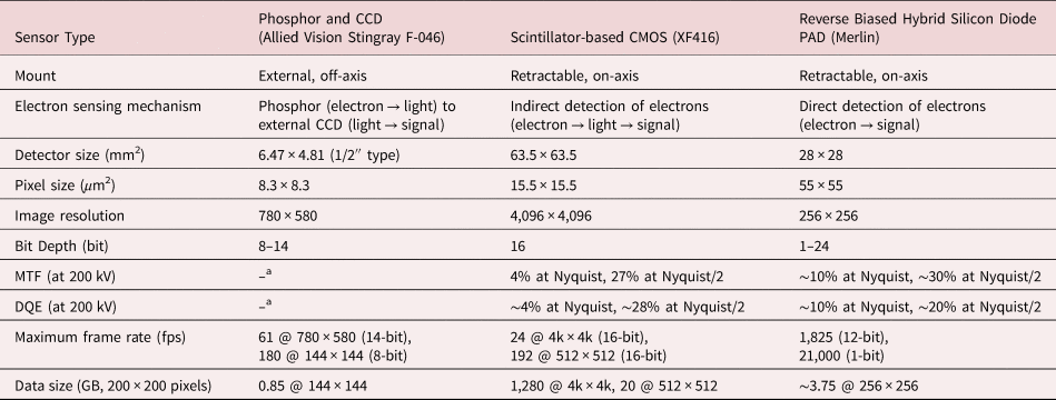
Image resolution and dynamic range can be adapted to a purpose (e.g., easy handling of a dataset).
a Note that MTF and DQE are not provided for Stingray CCD because this camera is designed for capturing visible light.
It is worth comparing the CMOS detector and hybrid silicon diode PAD. While image resolution is less important for orientation and phase indexing, dynamic range, electron sensitivity, and signal-to-noise ratio are crucial parameters. The performance of a detector is quantified by the modulation transfer function (MTF) and detective quantum efficiency (DQE) (Clough et al., Reference Clough, Moldovan and Kirkland2014). The MTF and DQE are a function of spatial frequency from 0 to 0.5/pixel. The upper limit is known as the Nyquist frequency, which corresponds to a reciprocal of twice the pixel size and is the largest possible frequency obtainable by a pixelated image. In most cases, a PAD shows higher performance because diffracted electrons are directly counted and converted as a signal with a larger pixel pitch (55 × 55 μm2) in the detector (direct electron detector). The signal is generated in the active layer and then the electrons exit the active layer before significant lateral scattering occurs (Tate et al., Reference Tate, Purohit, Chamberlain, Nguyen, Hovden, Chang, Deb, Turgut, Heron, Schlom, Ralph, Fuchs, Shanks, Philipp, Muller and Gruner2016). Scintillator-based CMOS systems show a lower performance because diffracted electrons are first converted to photons in the scintillator, and then those are detected by the CMOS after photons have passed through the optical fiber bundle for each pixel pitch (15.5 × 15.5 μm2) (indirect electron detector). Therefore, a PAD has an advantage to detect diffracted electrons especially under low dose conditions, because it has a higher electron sensitivity based on the fundamentally different sensor structure.
However, when the acceleration voltage is increased to 200 kV, a fall-off in the MTF and DQE is observed in both detectors. This problem is more pronounced in PAD because higher energy electrons spread further sideways in the Si sensor layer than lower-energy ones (Mir et al., Reference Mir, Plackett, Shipsey and Dos Santos2017b; Plotkin-Swing et al., Reference Plotkin-Swing, Corbin, De Carlo, Dellby, Hoermann, Hoffman, Lovejoy, Meyer, Mittelberger, Pantelic, Piazza and Krivanek2020). This means the performance gap between the two detectors closes with increased acceleration voltage. In the case of DQE, the performance of CMOS is comparable to that of PAD at 200 kV although the CMOS detector used in this study exhibits a larger Nyquist limit for a certain camera length (i.e. the image resolution is 4k × 4k for CMOS and 256 × 256 for PAD and the size of the detector is 63.5 × 63.5 mm2 for CMOS and 28 × 28 mm2 for PAD) (Table 1). Furthermore, the background intensity induced by inelastically scattered electrons could be reduced by using an in-column energy filter (Ramachandra et al., Reference Ramachandra, Bouwer, Mackey, Bushong, Peltier, Xuong and Ellisman2014). In addition, conventional microscopy such as dark-field imaging and diffraction analysis can be performed using the same detector while the previous study required the additional installation of a direct electron detector for a dedicated SPED experiment (Moeck et al., Reference Moeck, Rouvimov, Rauch, Véron, Kirmse, Häusler, Neumann, Bultreys, Maniette and Nicolopoulos2011; MacLaren et al., Reference MacLaren, Frutos-Myro, McGrouther, McFadzean, Weiss, Cosart, Portillo, Robins, Nicolopoulos, Nebot del Busto and Skogeby2020).
Following the significant improvement of orientation analysis shown in the present study, the on-axis CMOS system has further potential to be used for other applications. In practice, the highly binned diffraction patterns are enough to index the orientation (Rouvimov et al., Reference Rouvimov, Rauch, Moeck and Nicolopoulos2009; Rauch et al., Reference Rauch, Portillo, Nicolopoulos, Bultreys, Rouvimov and Moeck2010; Eggeman et al., Reference Eggeman, Krakow and Midgley2015). However, if the material consists of multiple phases with similar lattice parameters, using the CMOS detector at full resolution may be useful to provide an even more reliable orientation map, because slight differences in the positions of reflections could be resolved. Following a similar argumentation, in strain measurements, a higher resolution of the diffraction patterns could provide an improved strain resolution. A remaining challenge lies in the analysis of such large datasets, which can exceed 1 TB in size (Spurgeon et al., Reference Spurgeon, Ophus, Jones, Petford-Long, Kalinin, Olszta, Dunin-Borkowski, Salmon, Hattar, Yang, Sharma, Du, Chiaramonti, Zheng, Buck, Kovarik, Penn, Li, Zhang, Murayama and Taheri2020). Currently, several Python-based packages (de la Peña et al., Reference de la Peña, Ostasevicius, Fauske, Burdet, Prestat, Jokubauskas, Nord, Sarahan, MacArthur, Johnstone, Taillon, Caron, Migunov, Furnival, Eljarrat, Mazzucco, Aarholt, Walls, Slater, Winkler, Martineau and Donval2018; Clausen et al., Reference Clausen, Weber, Caron, Nord, Müller-Caspary, Ophus, Dunin-Borkowski, Ruzaeva, Chandra, Shin and van Schyndel2019; Savitzky et al., Reference Savitzky, Zeltmann, Barnard, Brown, Henderson and Ginsburg2019; Duncan et al., Reference Duncan, Phillip, Magnus, Joonatan, Simon, Eirik, Ben, Carter, Tina, Eric, Stef, Sean, Ida, Tom, Daen, Niels, Endre, Andrew, Timothy, Håkon, Jędrzej, Tiarnan, Tomas and Rob2020) are being developed to process such a large dataset (Paterson et al., Reference Paterson, Webster, Ross, Paton, Macgregor, McGrouther, MacLaren and Nord2020), which will lead to improved treatment of the 4D-STEM orientation data and also hold great potential for developing advanced orientation indexing approaches.
Conclusion
We demonstrate a PED-assisted 4D-STEM technique for orientation mapping using spot patterns captured by a fast, scintillator-coupled CMOS detector. While the orientation map obtained by the conventional system shows mis-indexed data points and scanning noise, the data acquisition with the high-resolution CMOS detector strongly suppresses these artifacts because the image quality of the diffraction patterns was improved by fast readout rate and high dynamic range of the detector. Moreover, the angular resolution of misorientation measurement could also be improved by optimizing the template matching process with weak reflections at high scattering angle, a large number of templates, and high image resolution of diffraction patterns. Based on the above advantages, fine details such as nano-sized grains, nanotwins, and sub-grain boundaries are resolved in the orientation map.
Supplementary material
To view supplementary material for this article, please visit https://doi.org/10.1017/S1431927621012538
Acknowledgments
This work was supported by the Max Planck Society. The authors thank Dr. Viswanadh Gowtham Arigela for providing Cu–Ag thin foils. G.D. acknowledges financial support by the ERC Advanced Grant GB-Correlate (Grant Agreement: 787446).


 Open access