


Introduction
Future 5G communication enables higher data rates, low latency, and even more services compared with current standards such as 4G. The need for higher data rate results in an increasing demand of bandwidth, which can be satisfied by choosing a higher operation frequency. The power amplifier (PA) is the most critical component in radio base stations since its performance strongly influences the overall system features in terms of bandwidth, output power, efficiency, and operating temperature. To ease a manufacturing of the amplifier circuit board surface-mount device (SMD) components and especially SMD housed transistors are widely used for mass market designs. With increasing frequency, the package parasitics become dominant and limit a possible wide-band matching.
The achievements in moderngallium-nitride (GaN) technology result in a high power density, high efficiency, and small device size which reduce parasitics and, therefore, simplify broadband designs in conjunction with high operation voltages. Therefore, GaN technology plays a major role for future communication systems. Numerous broadband PA designs based on GaN-high-electron-mobility transistors (HEMTs) have been published during the last years [Reference Zhu, Cheng and Yan1–Reference Tanany3]. However, preferably un-packaged GaN-HEMT bare-dies are used to minimize the device parasitics and therefore ease the design process [Reference Sayed, Tanany and Boeck4–Reference Andersson6]. A detailed description of mounting tolerances towards higher frequencies is given in [Reference Maassen7]. Hence, an increasing mounting effort needs to be utilized that results in the higher fabrication costs compared with SMD housed devices.
This contribution is an extension and further work of [Reference Drews8,Reference May9] and reflects the design and realization of two high-efficient broadband PAs for the S- and C-band frequency range. Herein, a design methodology for octave bandwidth PAs is presented utilizing DFN packaged devices. Followed by this introduction, preliminary design considerations are shown in the section ‘Design considerations’ including device analysis in relation to the package parasitics and a harmonic matching methodology. Inthe section ‘Design and realization’ the design procedure for the matching networks is presented. The realization and experimental results, continuous wave (CW), and modulated measurements, are discussed in the section ‘Experimental results’. A conclusion and comparison with state of the art PAs are given in the section ‘Conclusion’.
Design considerations
The two power devices CGH40006S (400 nm) and CGHV1F006S (250 nm) from Wolfspeed, which are designed as a surface mount dual-flat-no-lead (DFN) package, have been chosen for the design of the two wide-band power amplifiers. The recommended maximum frequency of operation is 6 GHz for the 400 nm and 15 GHz for the 250 nm technology. The devices are housing their corresponding bare-dies CGH60008D and CGHV1J006D, respectively. Both devices have been analyzed regarding the package influence for the same operating voltage at V DS = 36 V and a quiescent current of I Q = 100 mA and 60 mA, respectively.
Device analysis
The influence of the parasitic elements of the packages is stated in Fig. 1. Assuming a centered mounting of the bare-die, within the package, leads to equal parasitic effects for the in- and output. Bondwire connections between the pads of the package and bare-die are introducing a large inductance, but they are indispensable for the realization of the device. A mechanical device size of 920 μm and package dimensions of 3 × 3 mm2 (CGH40006S) result in a bondwire length of at least 1 mm without considering its loop. In contradiction to bare-die devices, the distance between the matching network and the transistor cannot be reduced to a minimum.
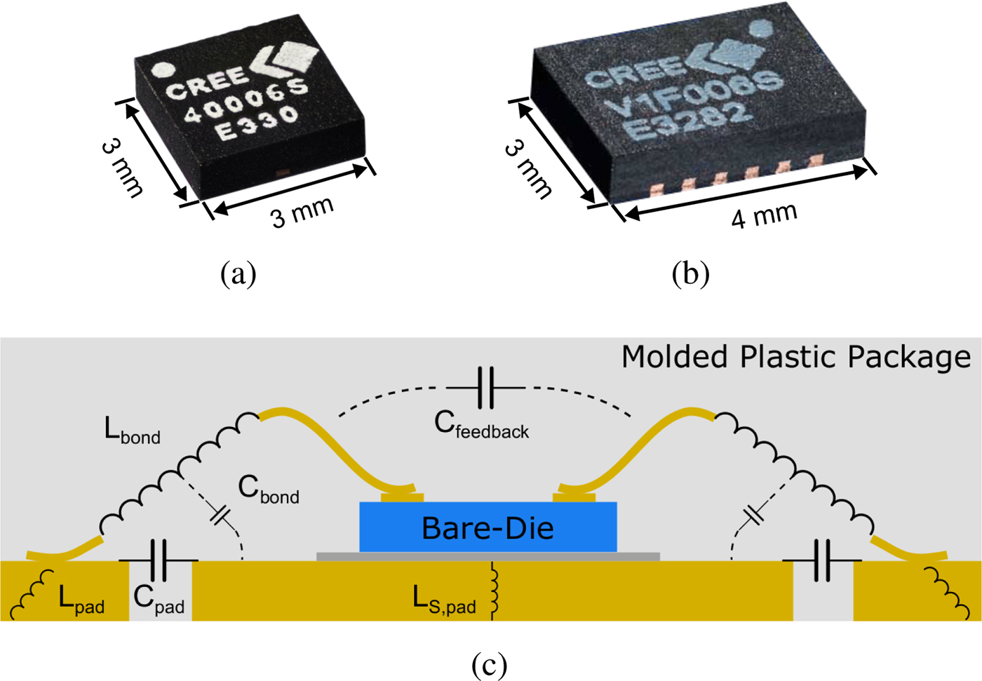
Fig. 1. Photographs of the packaged devices (a) CGH40006S, (b) CGHV1F006S, and (c) sideview of a DFN package and the introduced parasitic elements.
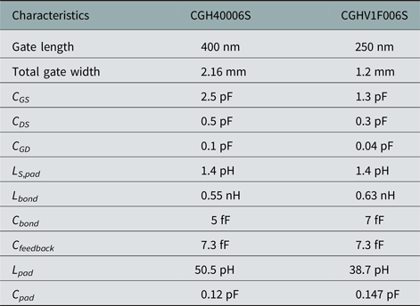
A detailed analysis taking the previous assumption into account was done using Keysight ADS. Table 1 states all relevant values for the elements of the packages. As can be seen, the bondwire inductance (L bond) and the related shunt capacitance (C bond) as well as the pad elements differ between the two devices. This fact is mainly caused by a slightly different package layout and bare-die dimensions. The 400 nm device is using one pad (0.4 × 0.3 mm2) for the connection of the signal path to the printed ircuit board, while the 250 nm device uses two of them with a smaller dimension of 0.2 × 0.4 mm2. Figure 2 depicts the difference between bare-die and packaged small-signal behavior of the output of the devices up to 10 GHz. The influence of the parasitic elements do have less influence for low frequencies but a transformation of the reflection coefficients into the inductive half plane of the smith chart occurs for the high-frequency range. This behavior is mainly caused by the bondwire inductance and complicates the matching of the devices.
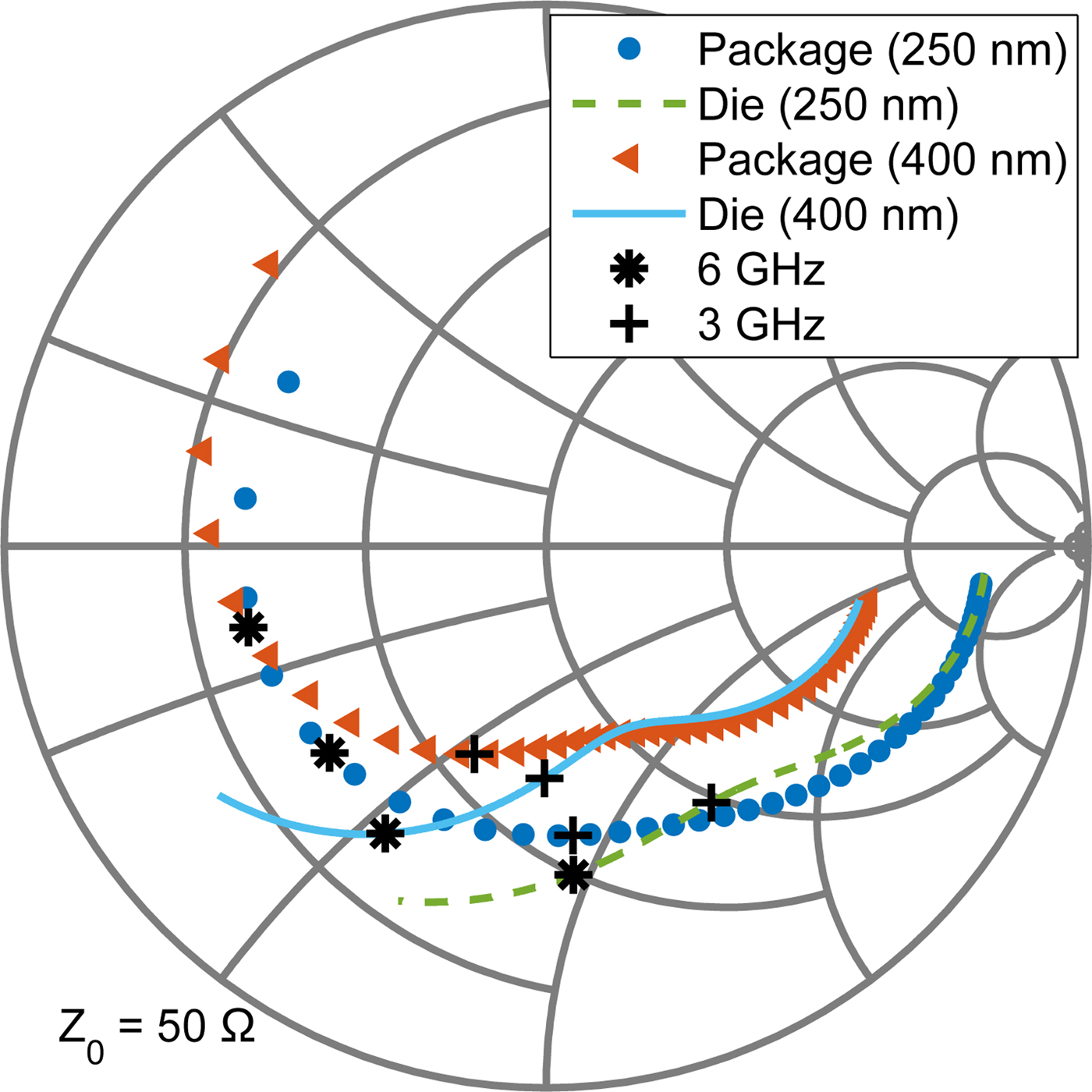
Fig. 2. S 22 for CGH40006S (V DS = 36 V, I Q = 100 mA) and CGHV1F006S (V DS = 36 V, I Q = 60 mA) in the frequency range from 0.1 to 10 GHz.
Table 1. Transistor-/ package-characteristics
To characterize the transistors under large-signal operation load- and source-pull simulations were carried out regarding maximum possible output power. The harmonic frequency components are hereby assumed to be an open circuit for the initial analysis. The results for the optimum reflection coefficients in the frequency range of 2–4 GHz for the CGH40006S at P out = 10 W and 4–8 GHz for the CGHV1F006S at P out = 5 W are shown in Fig. 3. As can be seen, the optimum output impedances are quite reasonable. In contradiction, the input side of the transistors are very low-ohmic. The package inductance transforms the impedances but as well spreads the trajectories, as can be noted for the in- and output. This behavior increases proportional to frequency and complicates a matching even further.
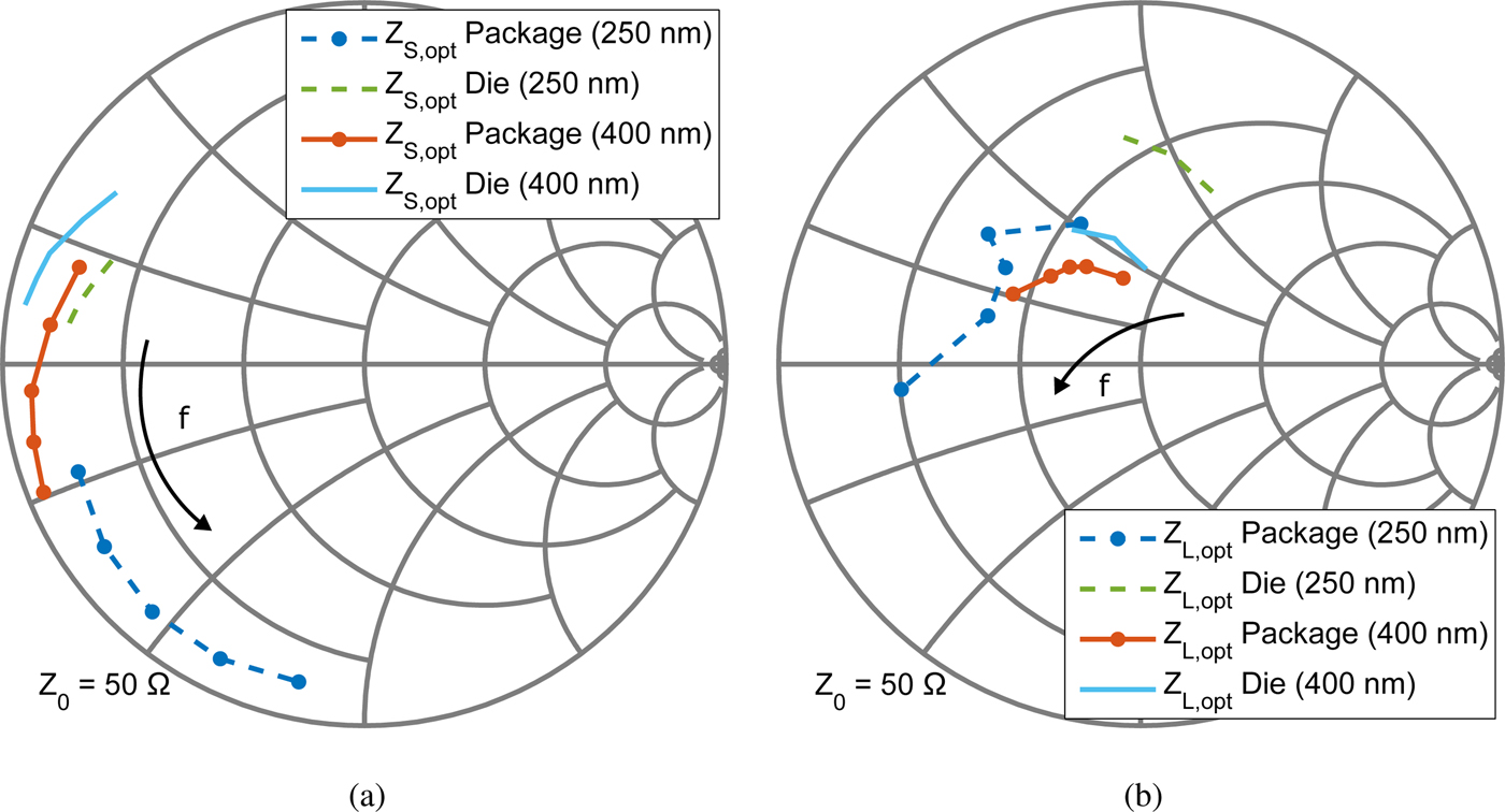
Fig. 3. Influence of the package in relation to (a) Z S,opt and (b) Z L,opt for CGH40006S (2–4 GHz) and CGHV1F006S (4–8 GHz) in comparison with the bare-dies of the corresponding technology (V DS = 36 V, I Q = 100/60 mA).
Harmonic matching methodology
The harmonic frequency components were assumed to be an open circuit during the initial load-pull analysis. This assumption will lead to serious problems for the design of octave bandwidth amplifiers because of the fact that the second harmonic for the lower frequency range is located within the band of interest. Changing the 2nd harmonic impedance from open to the optimum impedance at the upper band edge (Z f0,high) decreases P out and PAE for the fundamental frequency. Therefore, a special design procedure is needed similar to [Reference Tareq Arnous, Barbin and Boeck10].
The determined optimum load impedance for the high-frequency range are kept constant to achieve maximum P out. An additional second-tier load-pull simulation is performed for the low-frequency band edge considering the 2nd harmonic impedance. This leads to a slight modification of the initial impedances Z f0,low. Due to the fact that load-pull contours are tightening with the frequency as depicted inFig. 4 for an output power of 37 dBm, it follows that the selection of the low band impedances provides a higher degree of freedom in relation to P out. Hence, changing the impedance for low frequencies does have a negligible influence on the amplifier performance.
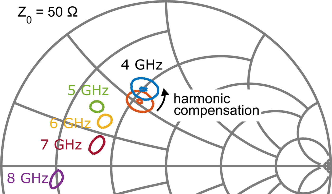
Fig. 4. Load-pull contours at 37 dBm output power for the CGHV1F006S with constant P out,max = 38 dBm in the frequency range of 4–8 GHz (V DS = 36 V, I Q = 60 mA).
Figure 5 states the influence of the 2nd harmonic phase on both devices and their performance at f 0 = 2 and 4 GHz for a constant magnitude of the reflection coefficient, which reflects the optimum impedance at the upper band edge. As can be seen, the resulting PAE and P out decrease drastically as soon as the optimum phase for the fundamental at high frequency is reached. The influence on the device performance is larger than 2 W for the 400 nm technology at f 0,low = 2 GHz. The involved PAE reduction is about 10%. A similar performance decrease can be noted for the 250 nm technology at f 0,low = 4 GHz.
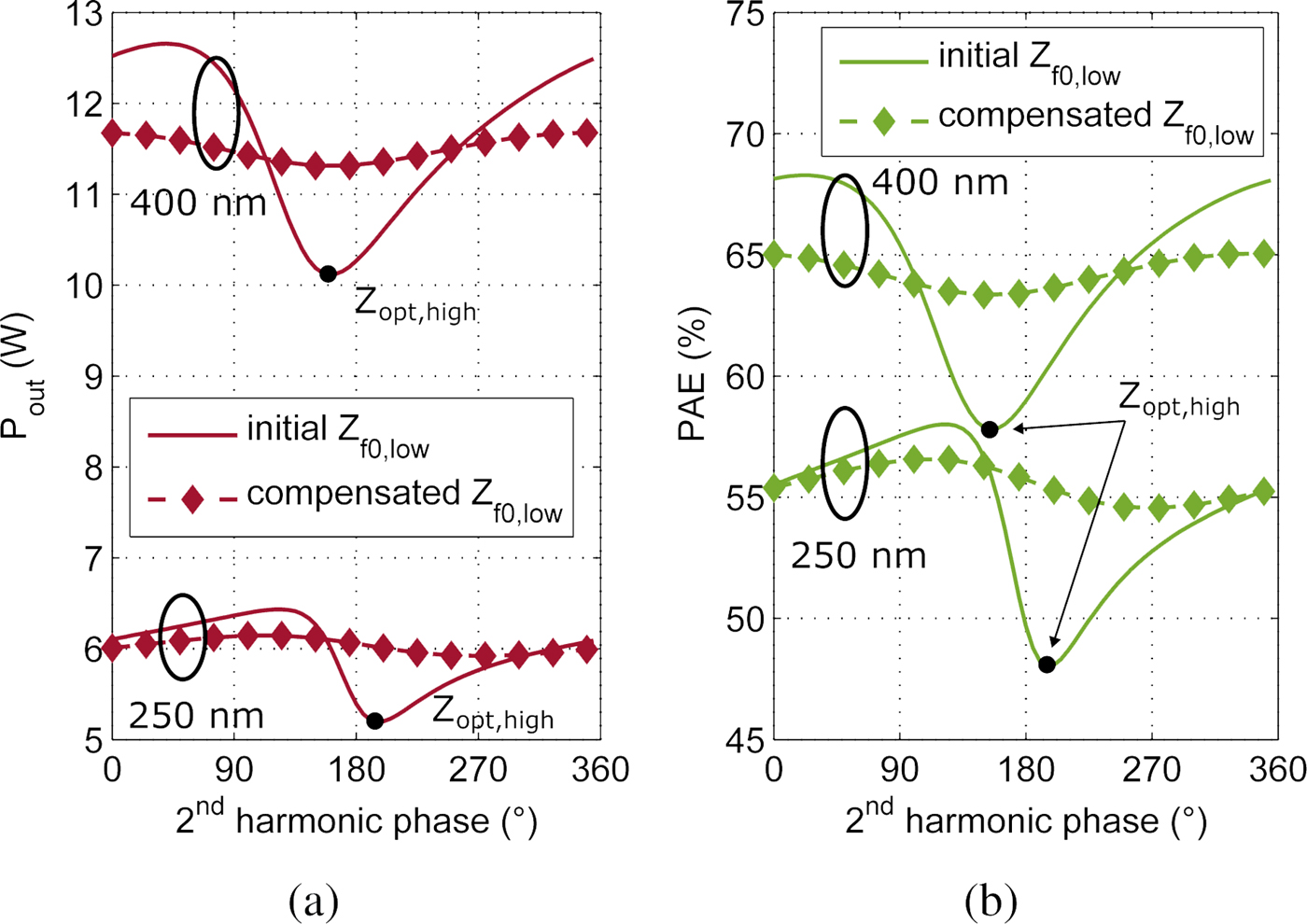
Fig. 5. Influence of the 2nd harmonic phase on (a) P out and (b) PAE with and without compensation of Z f0,low (V DS = 36 V, I Q = 100/60 mA).
This performance drop can be compensated by modifying the fundamental impedance towards a more inductive load (Fig. 4). As a consequence, the maximum possible output power at the introduced impedance Z mod,low is slightly decreasing but the performance in case of an optimal match for high frequencies (Z f0,high) is improved (Fig 5(a)). The same behavior can be noted for the PAE (Fig 5(b)). Hence, the influence of the harmonic matching on the fundamental frequency can be minimized.
This analysis of two different technologies proofs the functionality of the applied method. Further design considerations regarding the matching of the optimum load impedances Z L,opt for both devices will follow this approach.
Design and realization
The PAs are realized on Rogers RO4003c substrate with an increased via wall thickness for an improved thermal management. The substrate height is chosen to be 508 μm for the S-band design (PA S) and 221 μm for the C-band (PA C) design with a metalization of 35 μm. Figure 6 depicts a photograph of both prototypes and the schematics of the matching structures including characteristic impedances and electrical lengths.
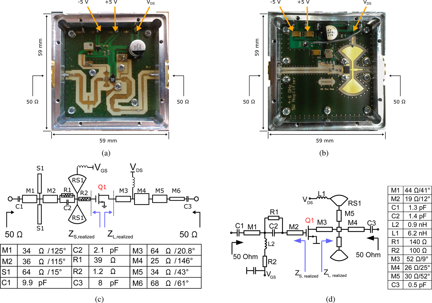
Fig. 6. Photographs of the realized amplifiers (a) PA S and (b) PA C including their (c), (d) circuit schematics.
Output matching network
The design goal of the amplifiers is to achieve the maximum available output power of the devices. The matching topology is based on a Chebyshev prototype low-pass filter [Reference Matthaei11]. While the theory only supports real-to-real transformation for the impedances the analyzed optimum impedances are complex. Therefore, a method of practically synthesizing real-to-real matching networks (MN) to real-to-complex MN was done, similar to [Reference Saad, Maassen and Boeck12].
The optimum output impedances for the S-band design are quite reasonable (Fig 3(b)). Hence, a stepped impedance transformer can simply achieve the required matching of the impedances to 50 Ω. In case of the C-band amplifier, a large shunt capacitance is necessary to resonate out the parasitic bondwire inductance, especially for high frequencies. Symmetrical radial stubs are implemented in front of the transistor to realize the broadband capacitors.
Input matching network
The input matching circuit is designed to provide a high and flat power gain within the required bandwidth. The large spreading of the trajectories of the optimum source impedances Z S,opt over the frequency makes wide-band matching difficult (Fig 3(a)). To overcome these limitations an increasing mismatch towards lower frequencies at the input of the transistors is created. Furthermore, the design procedure is chosen like inthe section ‘Output matching network’.
Small-signal stability for low frequencies is provided with a RC circuit in front of the transistor. An additional resistance is added at the Gate to stabilize the amplifier in the high-frequency band. Nonlinear stability analyses are performed to guarantee stability under large-signal conditions as presented in [Reference Dellier13].
Experimental results
In the experiments, the performance of the fabricated PAs was characterized under the conditions of small- and large-signal, i.e. CW and a modulated 5G signal. The PAs are biased to operate at V DS = 36 V and I q = 100 /60 mA.
Small-signal measurements
Figure 7 states the simulated and measured results of small-signal gain (S 21) as well as input return loss (S 11) of the prototypes. The simulation and measurements are found to be close to each other. The gain for PA S is larger than 14 dB within the desired bandwidth from 2 to 4 GHz. The response is slightly shifted in frequency and the gain is reduced to higher frequencies due to an increased inductance caused by the solder joints of the stabilization resistors. A carefully performed post-analysis shows that this behavior can be compensated by distributing the resistance of 1.2 Ω on three instead of two resistors. PA C provides a flat gain of more than 12 dB within the bandwidth of operation from 4 to 8 GHz. The relatively poor input return loss of about 3 dB for both devices is mainly due to the fact that the input matching network is designed to provide a flat gain.
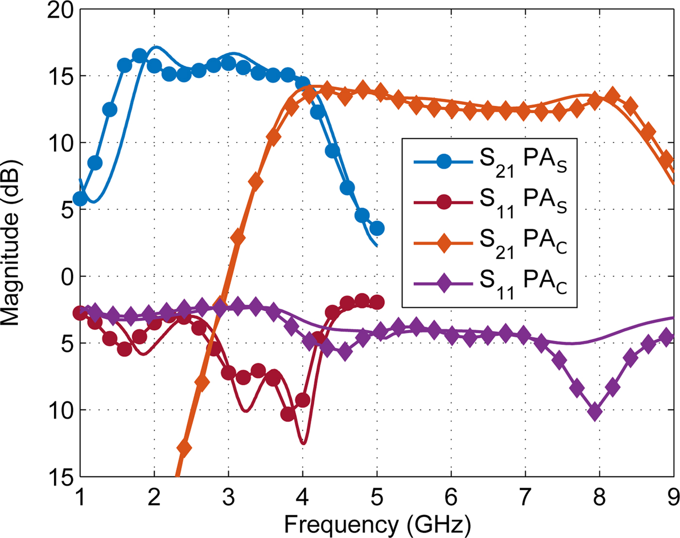
Fig. 7. Comparison between small-signal simulation (solid lines) and measurement results (symbols) for both PAs (V DS = 36 V, I Q = 100/60 mA).
Large-signal measurements
The large-signal analyses were done in an automated measurement environment. A pre-amplifier with a gain of 25 and 30 dBm output power is necessary to drive the realized PAs into saturation. Low loss directional couplers were used for measuring input and output power simultaneously in an automated measurement environment. Low pass filters were added to suppress the harmonic influence in the power measurement. A calibration of the setup guarantees a constant input power over frequency.
Figure 8 demonstrates a detailed view of the CW measurement results for PA S. At 28 dBm input power the output power performance is about 40–41 dBm in the frequency range from 1.9 to 4.2 GHz. The power gain is flat at 11 dB with a variation of ±0.5 dB and a PAE higher than 40% with peak-values up to 60%. As mentioned before, the parasitic inductance of the stabilization resistors at the Gate is degrading the large-signal performance as well [Reference Drews8]. This is the reason for the PAE-drop below 50% for frequencies beyond 3.5 GHz.
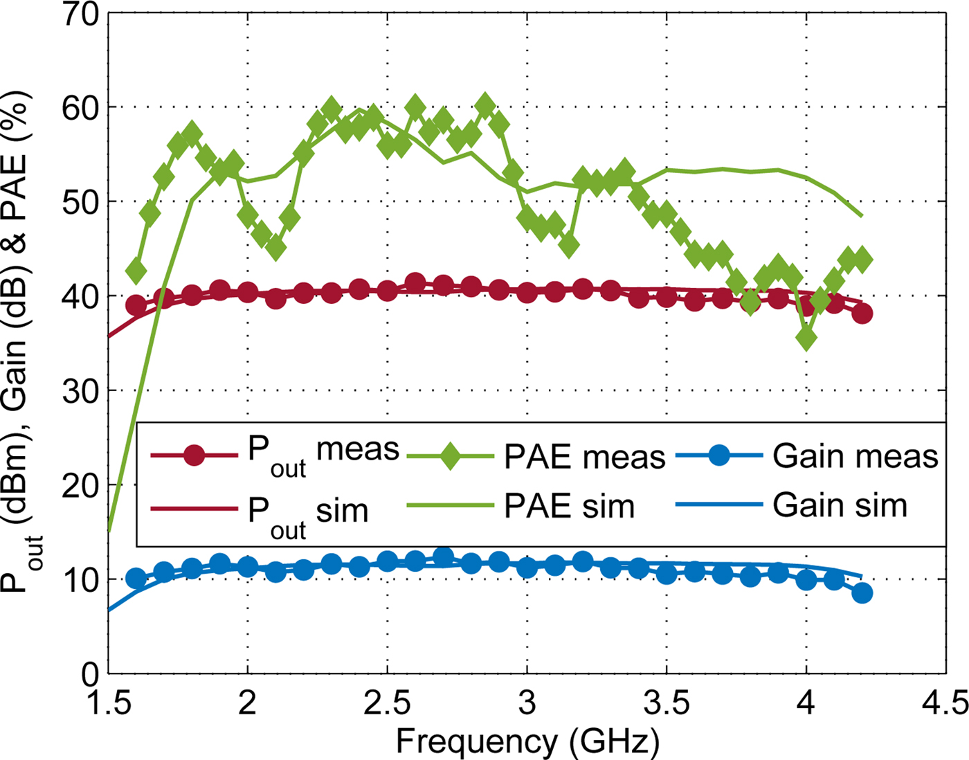
Fig. 8. Large-signal simulation (solid lines) and measurement results (symbols) versus frequency at 28 dBm input power for PA S (V DS = 36 V, I Q = 100 mA).
Experimental results for PA C are depicted in Fig. 9. Saturation is reached at P in = 28 dBm. As can be seen, there are marginal discrepancies in performance between 6.5 and 8 GHz regarding gain and output power. This leads to a PAE-drop down to 26%. The reason can be found in an inhomogeneous re-flow process of the ground pad soldering caused by thermal vias. Furthermore, this causes a misalignment of the device relative to the matching circuits. A detailed investigation including a Monte-Carlo analysis regarding the package placement tolerances is discussed in [Reference May9]. The placement accuracy can be improved by pick&place process instead of re-flow soldering. The large-signal performance still shows an achieved output power of more than P out > 35.5 dBm with a power gain of about 9 dB and a PAE of at least 26% and peak values of more than 40%.
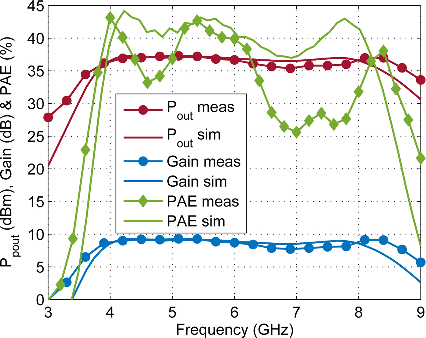
Fig. 9. Large-signal simulation (solid lines) and measurement results (symbols) versus frequency at 28 dBm input power for PA C (V DS = 36 V, I Q = 60 mA).
Nevertheless, a good agreement between simulation and measurement results is obtained for both prototype PAs. Mentioned deviations can get under control by automatic placement of the devices and the passive components.
Modulated signal measurements
Modulated measurements were performed to evaluate the inherent linearity of the PAs. In the evaluation, a complex 20 MHz 5G signal with 9.4 dB PAPR was used, which consists of 128 × 16QAM modulated subcarriers. The signal was generated using Keysight SystemVue and an E4438C vector signal generator. The PAs were measured with two different excitations, with and without RF-pre-distortion by Maxim Integrated which can handle up to 75 MHz signal bandwidth. The output signal was coupled out by an external directional coupler and fed back to the linearizer.
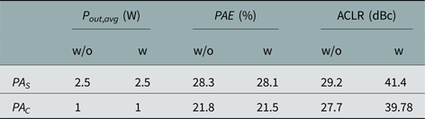
Figure 10 illustrates the measured spectral regrowth, before and after linearization of the 5G signal at P out,avg = 34 dBm for PA S and P out,avg = 30 dBm for PA C. The characteristics of the PAs for both cases are noticed in Table 2 in terms of average output power, average PAE, and minimum adjacent channel leakage ratio (ACLR). The measurements show that the PAs can be linearized to meet modern wireless communication system standards. The ACLR is improved by more than 12 dB resulting in at least 40 dBc while PAE and output power are keep at the same level for both excitations.
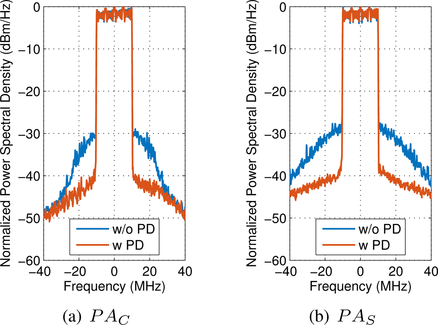
Fig. 10. Modulated measurements for a 20 MHz 5G signal at (a) 2.8 GHz for PA S and (b) 4 GHz for PA C (V DS = 36 V, I Q = 100/60 mA) with (w) and without (w/o) pre-distortion (PD), (a ) PA C, PA S.
Table 2. Modulated measurement results
Conclusion
In this work, a design methodology for octave bandwidth amplifiers and a solution for the in-band harmonic problem was discussed. Two-hybrid GaN-HEMT PAs were presented which demonstrates a wide-band performance about 75% fractional bandwidth in S- and C-band. Experimental results validate the design procedure. The measured results show a good agreement with simulation at a maximum output power of at least 10 W and 3.5 W for PA S and PA C, respectively. The in-house soldering process and the related misalignment of the transistor package causes a degradation in PAE for PA C at the frequencies in the range of 6.5–8 GHz. This issue can be resolved with the use of a pick & place process, which will lead to a more reliable alignment.
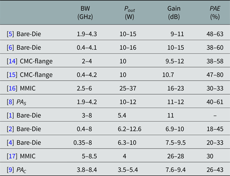
The obtained results are summarized in Table 3 in comparison with previously reported PAs. Low-cost DFN packaged GaN-HEMT transistors have been used within the design. Therefore, the active devices suffer from higher parasitics compared e.g. to [Reference Ulusoy2,Reference Saad5,16,17]. Nevertheless, both designs are highly competitive in comparison with other work. The achieved results with respect to bandwidth, gain and PAE are on one level with state-of-the-art work or even exceed this level. Moreover, the DFN-package offers simplified and reliable manufacturing due to the low mounting effort.
Table 3. State-of-the-art PAs
Furthermore, linearity has been observed using a complex modulated 5G signal and a modern pre-distortion technique. The measurements prove that the PAs can be linearized to meet future wireless communication system standards. The high bandwidth of the PAs enables multi-standard communication data transmission.
Acknowledgments
The authors would like to thank GloMic GmbH for their continuous support and advice.
 Felix Rautschke was born in Chemnitz, Germany. He received the B.Sc. degree, 2012, and the M.Sc. degree, 2014, in electrical engineering at the Chemnitz University of Technology. He is currently working towards the Ph.D. degree in the Microwave Engineering Research Laboratory at the Berlin Institute of Technology. His research interest is the area of broadband GaN microwave amplifier design.
 Stefan May was born in Aachen, Germany. He received the B.Eng. degree in electrical engineering from the University of applied Science in Aachen, Germany, in 2014, and the M.Sc. degree in electrical engineering from the Berlin University of Technology, Germany, in 2016. He is currently working as a hardware engineer at u-blox Berlin GmbH developing wireless communication modules for solutions for the Internet of Things.
 Sebastian Drews was born in Neubrandenburg, Germany. He received the B.Eng. degree in industrial engineering with focus on electrical engineering from the University of applied Science in Münster, Germany, 2012. The M.Sc. degree in electrical engineering from the Berlin Institute of Technology, Germany, in 2017. He is currently working as a research assistant in the Microwave Engineering Research Laboratory at the Berlin Institute of Technology.
 Daniel Maassen received the B.Eng. degree in electrical engineering from the University of applied Science in Aachen, Germany, in 2012, the M.Sc. degree in electrical engineering from the Berlin Institute of Technology, Germany, in 2014. He is currently working towards the Ph.D. degree in the Microwave Engineering Research Laboratory at Berlin Institute of Technology. His research concerns the design of efficient PAs as well as system components.
 Georg Boeck received the doctoral degree from the Berlin University of Technology, Berlin, Germany with honors, in 1984. In the same year, he joined Siemens Research Laboratories, Munich, Germany, where his research areas concerned fiber optics and GaAs electronics. Since 1991, he has been head of the Chair in Microwave Engineering with the Berlin Institute of Technology, Berlin, Germany. His areas of research involve the design and modeling of devices and circuits for high-efficiency power amplifiers and smart transceiver systems for modern digital communications technologies. He chaired several international conferences, served in numerous steering and technical program committees and editorial boards of respected international journals. From 2006 to 2008, he was recognized from the IEEE MTT society as ‘Distinguished Microwave Lecturer’ and was appointed as a guest professor at Southeast University Nanjing, Nanjing, China. Prof. Boeck is a Fellow of the IEEE.


