


Introduction
Transmission electron microscopy is a powerful tool for studying atomic-scale phenomena due to its unmatched spatial resolution and ability to perform imaging, diffraction, and multiple types of spectroscopic measurements (Egerton et al., Reference Egerton2005; Carter & Williams, Reference Carter and Williams2016; Zuo & Spence, Reference Zuo and Spence2017). Scanning TEM (STEM) is a particularly versatile TEM technique, as the STEM probe size can be tuned to any desired experimental length scale, from sub-Ångstrom to tens of nanometers, to best match the length scale of the structures being probed (Pennycook & Nellist, Reference Pennycook and Nellist2011). The size of the probe is also completely decoupled from the step size between adjacent probe positions, allowing experimental fields of view up to almost 1 mm2 (Kuipers et al., Reference Kuipers, Kalicharan, Wolters, van Ham and Giepmans2016). Advances in detector technology have lead to high-speed electron cameras capable of recording full 2D images of the diffracted STEM probe with microsecond-scale dwell times, which has lead to many experiments which record the full four-dimensional (4D) dataset, in a family of methods called 4D-STEM (Ophus, Reference Ophus2019). In parallel, the rise of powerful computational methods have enabled measurements of many different material properties with high statistical significance (Spurgeon et al., Reference Spurgeon, Ophus, Jones, Petford-Long, Kalinin, Olszta, Dunin-Borkowski, Salmon, Hattar, Yang, Sharma, Du, Chiaramonti, Zheng, Buck, Kovarik, Penn, Li, Zhang, Murayama and Taheri2021).
The combination of computational methods and advanced STEM experimentation has lead to atomic-resolution 3D tomographic reconstructions (Yang et al., Reference Yang, Chen, Scott, Ophus, Xu, Pryor, Wu, Sun, Theis, Zhou, Eisenbach, Kent, Sabirianov, Zeng, Ercius and Miao2017), measurements of highly beam-sensitive samples over functional length scales (Panova et al., Reference Panova, Ophus, Takacs, Bustillo, Balhorn, Salleo, Balsara and Minor2019), images of samples with resolution better than the diffraction limit (Chen et al., Reference Chen, Jiang, Shao, Holtz, Odstrčil, Guizar-Sicairos, Hanke, Ganschow, Schlom and Muller2021), and many other advances in STEM imaging techniques. Many of the technique developments and validation of these experiments make heavy use of electron scattering simulations. The application of data-intensive machine learning methods to STEM experiments can also be aided by simulations (Kalinin et al., Reference Kalinin, Ophus, Voyles, Erni, Kepaptsoglou, Grillo, Lupini, Schwenker, Chan, Etheridge, Li, Han, Ziatdinov, Shibata and Pennycook2021).
It is possible to simulate the propagation and scattering of STEM probes through a material by directly computing the Bloch wave eigenstates of the electron scattering matrix ( ${\cal S}$-matrix) (Bethe, Reference Bethe1928). The Bloch Wave method can be employed in diffraction simulations (Zuo et al., Reference Zuo, Zhu, Ang and Shah2021), but it is only practical to use for small, periodic unit cells. The majority of the STEM simulations performed currently implement the multislice method (Cowley & Moodie, Reference Cowley and Moodie1957). The multislice method is typically applied in STEM simulations by performing a separate quantum-mechanical electron scattering simulation for each probe position (Croitoru et al., Reference Croitoru, Van Dyck, Van Aert, Bals and Verbeeck2006; Okunishi et al., Reference Okunishi, Sawada and Kondo2012; Ophus et al., Reference Ophus, Ciston, Pierce, Harvey, Chess, McMorran, Czarnik, Rose and Ercius2016). The multislice algorithm can therefore require extremely large computation times when simulating STEM experiments which can contain 1,0002 probe positions or even higher. To alleviate this issue, various authors have implemented parallelized simulation codes that make use of multiple central processing unit (CPU) or graphics processing unit (GPU) resources (Grillo & Rotunno, Reference Grillo and Rotunno2013; Allen et al., Reference Allen, D'Alfonso and Findlay2015; Hosokawa et al., Reference Hosokawa, Shinkawa, Arai and Sannomiya2015; Van den Broek et al., Reference Van den Broek, Jiang and Koch2015; Kirkland, Reference Kirkland2016; Lobato et al., Reference Lobato, Van Aert and Verbeeck2016; Oelerich et al., Reference Oelerich, Duschek, Belz, Beyer, Baranovskii and Volz2017; Barthel, Reference Barthel2018; Radek et al., Reference Radek, Tenberge, Hilke, Wilde and Peterlechner2018).
It is possible to perform large STEM simulations more efficiently by computing them as a superposition of plane waves (Chen et al., Reference Chen, Van Dyck, De Beeck, Broeckx and Van Landuyt1995). This idea was developed into an efficient simulation algorithm by Ophus (Reference Ophus2017), who named it the plane-wave reciprocal-space interpolated scattering matrix (PRISM) algorithm. In the PRISM algorithm, the  ${\cal S}$-matrix elements are directly computed by multislice simulations. The equivalence of the Bloch wave ${\cal S}$-matrix and multislice simulation outputs have been investigated in detail by Allen et al. (Reference Allen, Findlay, Oxley and Rossouw2003) and Findlay et al. (Reference Findlay, Allen, Oxley and Rossouw2003). The PRISM algorithm has been implemented into multiple simulation codes (Pryor et al., Reference Pryor, Ophus and Miao2017; Brown et al., Reference Brown, Pelz, Ophus and Ciston2020a; Madsen & Susi, Reference Madsen and Susi2020). It has also been extended to a double- ${\cal S}$-matrix formalism which can provide an even higher speed boost relative to multislice for inelastic scattering such as in STEM electron energy loss spectroscopy (STEM-EELS) simulations (Brown et al., Reference Brown, Ciston and Ophus2019).
The PRISM algorithm achieves large decreases in calculation times by reducing the sampling of the probe wavefunction in reciprocal space and is highly accurate when the detector configuration is given by large monolithic regions. However, PRISM simulations are less accurate where fine details in the STEM probe and diffracted Bragg disks are necessary, for example, in Juchtmans et al. (Reference Juchtmans, Béché, Abakumov, Batuk and Verbeeck2015), Hubert et al. (Reference Hubert, Römer and Beanland2019), and Zeltmann et al. (Reference Zeltmann, Müller, Bustillo, Savitzky, Hughes, Minor and Ophus2020). A different form of interpolation has been proposed by Pelz et al. (Reference Pelz, Brown, Findlay, Scott, Ciston and Ophus2020a), where the STEM probe is partitioned into different beams by the interpolation of basis functions constructed from the initial STEM probe. This partitioning of the probe has been shown to be a highly efficient and accurate representation of dynamical scattering of the STEM probe in experimental data and is fully compatible with the PRISM algorithm (Pelz et al., Reference Pelz, Brown, Ciston, Findlay, Zhang, Scott and Ophus2020b).
In this manuscript, we introduce the partitioned PRISM algorithm for use in STEM simulations. We describe the theory of multislice, PRISM, and partitioned PRISM simulations and provide a reference implementation of these algorithms. We show that beam partitioning simulations provide an excellent trade off between calculation times and accuracy by measuring the error of diffracted STEM probes with respect to multislice simulations as a function of the number of included beams. We also use this method to simulate the full field of view for a common experimental geometry, a metal nanoparticle resting on an amorphous substrate. These simulations demonstrate that the partitioned PRISM method can produce comparable accuracy for coherent diffraction to PRISM simulations, but for much lower calculation times and lower random access memory (RAM) usage. This is important since many PRISM simulations are constrained by the available RAM of a GPU to hold the  ${\cal S}$-matrix. Finally, we demonstrate the utility of this method in 4D-STEM simulations by simulating the full 4D dataset of an extremely large (5122 probes, 4.6 million atoms) sample cell and measuring the sample strain, where the partitioned PRISM algorithm provides superior performance to a PRISM simulation using roughly the same total calculation time.
Theory
For previously published TEM simulation methods, we will briefly outline the required steps here. We refer readers to Kirkland (Reference Kirkland2020) for more information on these methods. We will also only describe the scattering of the electron beam while passing through a sample; probe-forming optics and the microscope transfer function mathematics are described in many other works (Williams & Carter, Reference Williams and Carter2009; Spence, Reference Spence2013; Kirkland, Reference Kirkland2020).
Elastic Scattering of Fast Electrons
Transmission electron microscopy simulations aim to describe how an electron wavefunction ψ(r) evolves over the 3D coordinates r = (x, y, z). The evolution of the slow-moving portion of the wavefunction along the optical axis z can be described by the Schrödinger equation for fast electrons (Kirkland, Reference Kirkland2020)
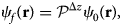
 $${\partial \over \partial z}\psi( {\bf r}) = {{{i\mkern 1mu}} \lambda\over 4 \pi} {\nabla_{xy}}^{2} \psi( {\bf r}) + {{i\mkern 1mu}} \sigma V( {\bf r}) \psi( {\bf r}) ,\; $$
where λ is the relativistic electron wavelength,  ${\nabla _{xy}}^{2}$ is the 2D Laplacian operator, σ is the relativistic beam-sample interaction constant, and V(r) is the electrostatic potential of the sample.
The Bloch Wave Algorithm
The Bloch wave method uses a basis set that satisfies equation (1) everywhere inside the sample boundary, which is assumed to be periodic in all directions. This basis set is calculated by calculating the eigendecomposition of a set of linear equations that approximate equation (1) up to some maximum scattering vector |q max|. Then, for each required initial condition (such as different STEM probe positions on the sample surface), we compute the weighting coefficients for each element of the Bloch wave basis. Finally, the exit wave after interaction of the sample is calculated by multiplying these coefficients by the basis set. This procedure can be written in terms of an  ${\cal S}$-matrix as Kirkland (Reference Kirkland2020)
 $$\psi_f( {\bf r}) = {\cal S} \psi_0( {\bf r}) ,\; $$
where ψ 0(r) and ψ f(r) are the incident and exit wavefunctions, respectively. The Bloch wave method can be extremely efficient for small simulation cells, such as periodically tiled crystalline materials. High symmetry is also an asset for Bloch wave simulations, as it allows the number of beam plane waves (beams) included in the basis set to be limited to a small number. However, for a large STEM simulation consisting of thousands or even millions of atoms in the simulation, the  ${\cal S}$-matrix may contain billions or more entries, which requires an impractical amount of time to calculate the eigendecomposition (roughly Θ(B 3) for B beams). Using equation (2), many times for multiple electron probes could require extremely large computational times. Thus, Bloch wave methods are only used for plane wave, diffraction, or very small size STEM simulations.
The Multislice Algorithm
The formal operator solution to equation (1) is given by Kirkland (Reference Kirkland2020),
 $$\psi_f( {\bf r}) = \exp \left\{\int_{0}^{z} \left[{i \lambda\over 4 \pi}\nabla^{2}_{xy} + i\sigma V( x,\; y,\; z') \right]dz' \right\}\psi_0( {\bf r}) ,\; $$
where ψ f(r) is the exit wavefunction after traveling a distance z from the initial wave ψ 0(r). This expression is commonly approximately solved with the multislice algorithm first given by Cowley & Moodie (Reference Cowley and Moodie1957), which alternates solving the two operators using only the linear term in the series expansion of the exponential operator.
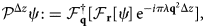
In the multislice algorithm, we first divide up the sample of total thickness t into a series of thin slices with thickness Δz. Solving for the first operator on equation (3) yields an expression for free space propagation between slices separated by Δz, with the solution given by
 $$\psi_f( {\bf r}) = {\cal P}^{\Delta z} \psi_0( {\bf r}) ,\; $$
where  ${\cal P}^{\Delta z}$ is the Fresnel propagator defined by
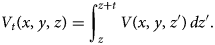
 $${\cal P}^{\Delta z}\psi\, \colon = {\cal F}_{\bf q}^{{\dagger}} [ {\cal F}_{\bf r} [ \psi ] \, {\rm e}^{-i \pi \lambda {\bf q}^{2} \Delta z}],\; $$
where q = (q x, q y) are the 2D Fourier coordinates and r = (x, y) are the 2D real-space coordinates.  ${\cal F}_{\bf x}[{\, \cdot \, }]$ denotes the two-dimensional Fourier transform with respect to x and ${\cal F}_{\bf x}^{{\dagger}} [{\, \cdot \, }]$ the 2D inverse Fourier transform with respect to x.
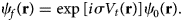
To solve for the second operator in equation (3), integrate the electrostatic potential of the sample over the slice of thickness t
 $$V_{t}( x,\; y,\; z) = \int_{z}^{z + t}V( x,\; y,\; z') \, dz'.$$
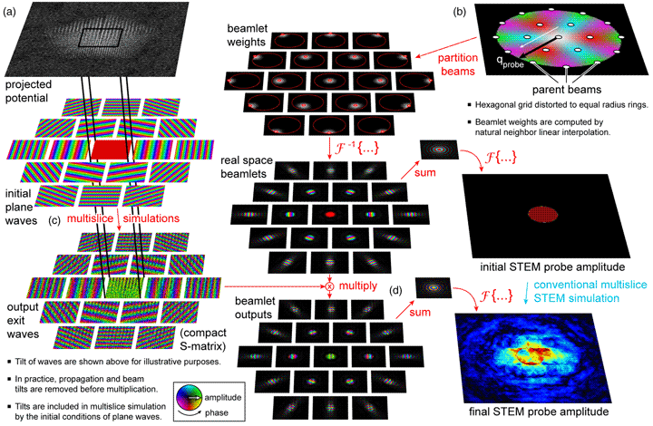
Figure 1a shows an example of this slicing procedure. If we assume that the electron scattering inside this slice occurs over infinitesimal thickness, the resulting solution to this operator is
 $$\psi_f( {\bf r}) = \exp[ {{i\mkern 1mu}} \sigma V_{t}( {\bf r}) ] \psi_0( {\bf r}).$$
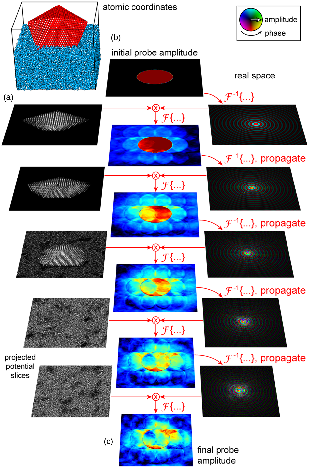
Fig. 1. The multislice simulation algorithm. (a) Calculate the projected potential slices from the atomic coordinates and lookup tables. (b) Initialize the probe wavefunction, and then alternate between propagation and transmission operators. (c) Final probe at the sample exit plane.
We can then write one iteration of the multislice algorithm as
 $${\cal T}( \psi,\; V_{k}) = {\cal P}^{t}[ \psi\cdot {\rm e}^{i\sigma V_{k}}] \, \colon = {\cal T}_k \psi,$$
where V k is the projected potential at slice k. This algorithm is shown schematically in Figure 1b. The multislice solution of a wavefunction ψ after k potential slices is then
 $${\cal M}^{V}_k \psi = \left\{\matrix{ \psi\cdot {\rm e}^{{{i\mkern 1mu}} \sigma V_{k}},\; \hfill & {\rm if } \quad k = 0\hfill \cr {\cal T}( {\cal M}_{k-1}^{V}\psi,\; V_{k}) ,\; \hfill & {\rm if }\quad k> 0 \hfill }\right.,$$
for which we introduce the short notation  ${\cal M}_k$ if the potential is assumed to be fixed. It is important to note that ${\cal T}( \psi ,\; V_{k})$ is linear in ψ and nonlinear in V k and thus
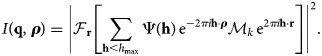
  ${\cal M}^{V}_k$ is linear in ψ and nonlinear in V. Traditionally, a STEM or 4D-STEM simulation was computed by shifting the incoming wave function to the scan positions ρ and computing the resulting far-field intensity using the multislice algorithm at each position:
 $$I( {\bf q},\; {\boldsymbol \rho}) = \vert {\cal F}_{\bf r}[{{\cal M}_k\psi( {\bf r}-{\boldsymbol \rho}) }] \vert ^{2}.$$
An example of this output is shown in Figure 1c. This requires us to perform a full multislice calculation at each scan position, which makes large fields of view that could contain millions of probe positions computationally expensive.
The PRISM Algorithm for STEM Simulations
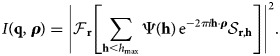
Recently, Ophus (Reference Ophus2017) proposed an elegant solution to this problem. The incident wave-function of a microscope in a scanning geometry usually passes through a beam-forming aperture with maximum allowed wave vector h max and is then focused onto the sample. It can therefore be described as
 $$\psi( {\bf r},\; {\boldsymbol \rho}) = \sum_{\vert {\bf h}\vert < h_{{\rm max}}}\Psi( {\bf h}) \, {\rm e}^{2 \pi {{i\mkern 1mu}} {\bf h}\cdot( {\bf r}-{\boldsymbol \rho}) },\; $$
with Ψ(h) the Fourier transform of ψ(r) and ρ the two-dimensional scan coordinate. Using the linearity of the multislice algorithm with respect to ψ and equation (11), we can then rewrite equation (10) as
 $$I( {\bf q},\; {\boldsymbol \rho}) = \left\vert {{\cal F}_{\bf r}\left[{\sum_{{\bf h}< h_{{\rm max}}}\Psi( {\bf h}) \, {\rm e}^{-2\pi i{\bf h}\cdot{\boldsymbol \rho}}{\cal M}_k \, {\rm e}^{2 \pi i{\bf h} \cdot{\bf r}}}\right]}\right\vert ^{2}.$$
We take equation (12) to link our algorithm to the existing Bloch wave literature in electron microscopy. Traditionally, the set h of incoming plane waves is referred to as “beams,” and the linear operator that maps from plane waves entering the sample to plane waves exiting the sample is referred to as the  ${\cal S}$-matrix. Using equation (12), we can define the real-space scattering matrix ${{\cal S_{{\bf r}, {\bf h}}}\, \colon = {\cal M}_k \, {\rm e}^{2 \pi i{\bf h}\cdot {\bf r}}}$, which is the set of exit waves produced by running the multislice algorithm on the set of plane waves present in the probe-forming aperture of the microscope. The scattering matrix encapsulates all amplitude and phase information that is required to describe a scattering experiment with variable illumination, given a fixed sample potential V.
Given the  ${\cal S}$-matrix and a maximum scattering angle h max in the condenser aperture, we can rewrite equation (12) with the real-space scattering matrix as
 $$I( {\bf q},\; {\boldsymbol \rho}) = \left\vert {{\cal F}_{\bf r}\left[{\sum_{{\bf h}< h_{{\rm max}}}\Psi( {\bf h}) \, {\rm e}^{-2 \pi i{\bf h}\cdot{\boldsymbol \rho}}{\cal S}_{{\bf r}, {\bf h}}}\right]} \right\vert ^{2}.$$
To introduce the concepts used in the PRISM algorithm, we now need to consider the variables r and h on a discretely sampled grid. The bandwidth-limitation |h| < h max means that the incoming probe is represented by a finite number of Fourier coefficients  ${{\bf h}_{{\sf b}} \in {\sf H} = { ( h_x,\; h_y) \, \vert \, \Vert {\bf h}\Vert _2< h_{{\rm max}}}}$. Let the discretely sampled ${\cal S}$-matrix have dimensions ${\cal S}_{{\bf r}, {\sf b}} \in {\opf C}^{{\sf N}_1 \times {\sf N}_2 \times {\sf B}}$, with ${\sf N}_1 \times {\sf N}_2$ the real-space dimensions and ${\sf B} = \vert {\sf H}\vert$ the number of pixels sampled in the condenser aperture.
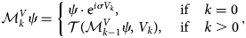
To compute the  ${\cal S}$-matrix, we run the multislice algorithm for each wavevector
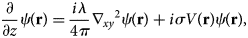
  ${\bf h}_{{\sf b}}$ that is sampled in the detector plane. These steps are shown schematically in Figures 2a and 2b. This strategy yields favorable computational complexity when a large number of probe positions needs to be calculated, which is necessary for large field-of-view STEM simulations. It has the additional advantage that a series of scanning diffraction experiments with different illumination conditions can be simulated without recomputing the ${\cal S}$-matrix. This method was named the PRISM algorithm by Ophus (Reference Ophus2017). It was first implemented into a simulation code parallelized for both CPUs and GPUs in the Prismatic implementation (Pryor et al., Reference Pryor, Ophus and Miao2017). Since then, the PRISM algorithm has also been implemented in the GPU simulations codes py_multislice (Brown et al., Reference Brown, Pelz, Ophus and Ciston2020a) and abTEM (Madsen & Susi, Reference Madsen and Susi2020). The PRISM algorithm introduced an additional concept to improve the scaling behaviour of STEM simulations via the scattering matrix. If only each fth beam in the condenser aperture is sampled, the field of view in real-space contains f 2 copies of the probe with size ${{\sf N}_1/f \times {\sf N}_2/f}$. If one of these probe copies is cropped out, and then the far-field intensities computed via equation (13), we can perform simulations that trade a small amount of accuracy for a significant speed-up in computation times (Ophus, Reference Ophus2017). The new model then reads
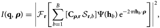 $$I( {\bf q},\; {\boldsymbol \rho}) = \left\vert {{\cal F}_{\bf r}\left[ {\sum^{{\sf B}}_{{\sf b = 1}}[ {\bf C}_{{\boldsymbol \rho}, {\bf r}}\, {\cal S}_{{\bf r}, {\sf b}}] \Psi( {\bf h}_{{\sf b}}) \, {\rm e}^{-2 \pi i{\bf h}_{{\sf b}}\cdot{\boldsymbol \rho}}} \right]}\right\vert ^{2},\;$$
where we have introduced a cropping operator
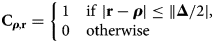 $${\bf C}_{{\boldsymbol \rho}, {\bf r}} = \left\{\matrix{ 1 \hfill & {\rm if }\; \vert {\bf r} - {\boldsymbol \rho}\vert \leq \Vert {\bf \Delta}/2\vert ,\; \hfill \cr 0 \hfill & {\rm otherwise} \hfill }\right.$$
with the absolute value | · | applied element-wise, a two-dimensional rectangular function of width  ${{\bf \Delta } \in {\opf R}^{{\sf N}_1 / f \times {\sf N}_2 / f}}$ centered about each probe scan position ρ. This cropping procedure to compute STEM probes using PRISM is shown in Figures 2c and 2d.
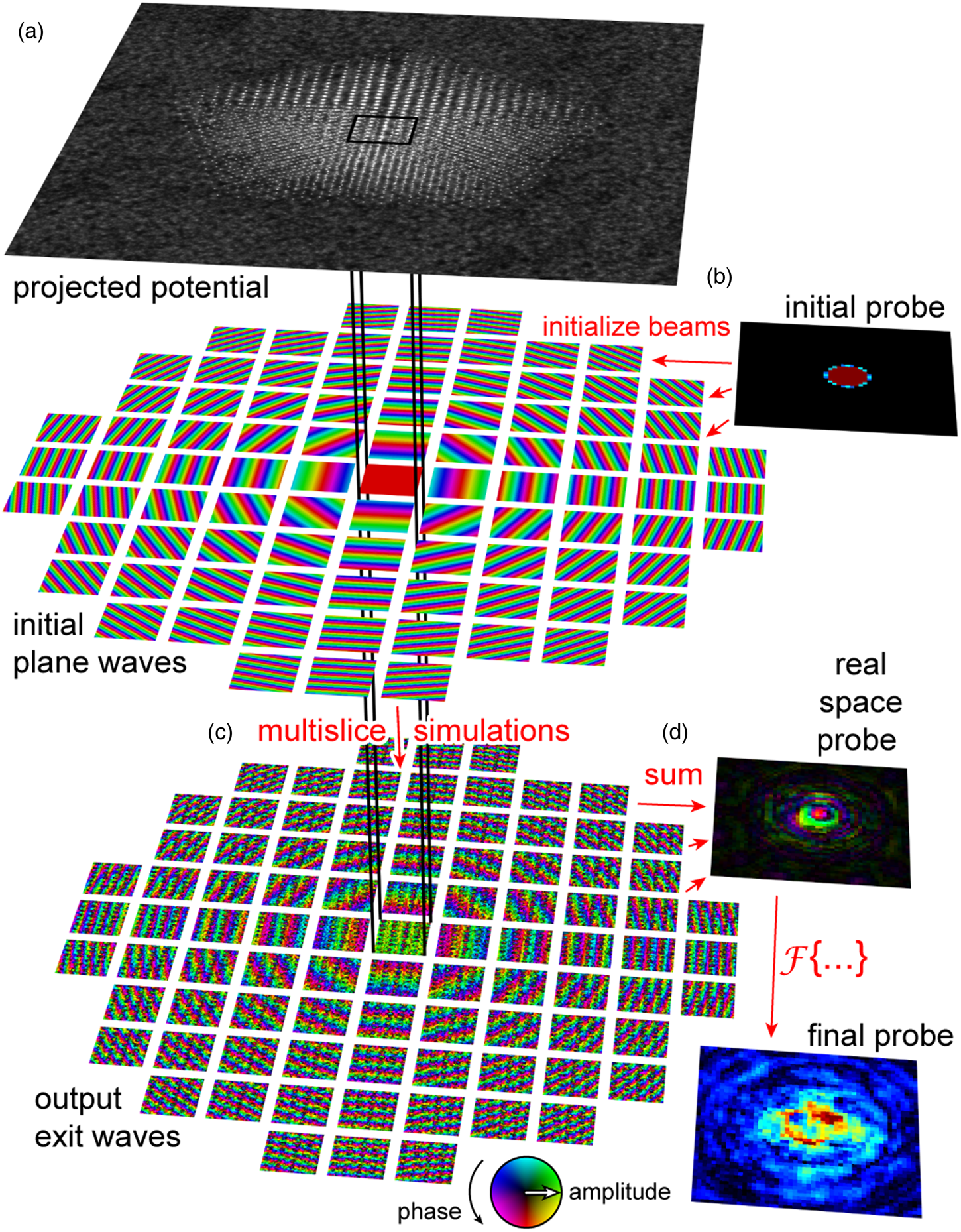
Fig. 2. The PRISM simulation algorithm. (a) Calculate the projected potential slices from the atomic coordinates and lookup tables. (b) Select an interpolation factor f and a maximum scattering angle |q max|, and initialize all tilted plane waves needed for these beams. (c) Perform a multislice simulation for each beam over the full field of view, store in the  ${\cal S}$-matrix. (d) Compute outputs by shifting the initial STEM probes and cropping 1/f of the total field of view, and multiplying and summing all ${\cal S}$-matrix beams.
The Partitioned PRISM Algorithm
Natural Neighbor Interpolation of the Scattering Matrix
Theoretical and experimental investigations of  ${\cal S}$-matrix reconstructions have shown that once the plane-wave tilts have been removed from all beams, the resulting matrix elements are remarkably smooth (Brown et al., Reference Brown, Pelz, Hsu, Zhang, Ramesh, Inzani, Sheridan, Griffin, Findlay, Allen, Scott, Ophus and Ciston2020b; Pelz et al., Reference Pelz, Brown, Ciston, Findlay, Zhang, Scott and Ophus2020b; Findlay et al., Reference Findlay, Brown, Pelz, Ophus, Ciston and Allen2021). We have also observed that in many PRISM simulations, the information contained in neighboring beams is very similar. These observations have inspired us to propose a new method for simulating STEM experiments. Rather than computing all beams of the ${\cal S}$-matrix with the multislice algorithm, we could instead interpolate them from a reduced set ${\cal P}$ of parent beams, which are computed with the multislice algorithm in the manner described above.
Defining the interpolation weights as a matrix  ${w \in {\opf R}^{\vert {\cal P}\vert \times B}}$ that stores the interpolation weights for each beam, we can then compute the 4D-STEM intensities as
 $$\eqalignb{I( {\bf q},\; {\boldsymbol \rho}) & = \left\vert {\cal F}_{{\bf r}}\left[\sum^{{\sf B}}_{{\sf b = 1}}\Psi( {\bf h}_{{\sf b}}) \, e^{-2 \pi i {\bf h}_{{\sf b}}\cdot{\boldsymbol \rho}}\right.\right.\cr & \quad \left. \left. \cdot {\bf C}_{{\boldsymbol \rho}, {\bf r}}\left[{\rm e}^{2 \pi i {\bf h}_{{\sf b}}\cdot{\boldsymbol r}}\sum_{{\sf p} \in {\cal P}}w_{{\sf p}, {\sf b}}\, {\rm e}^{-2 \pi i {\bf h}_{{\sf p}}\cdot{\boldsymbol r}}{\cal S}_{{\bf r}, {\sf p}}\right]\right]\right\vert ^{2}.}$$
Through numerical tests we found that the interpolation of the  ${\cal S}$-matrix beams at the exit surface can produce substantial relative errors compared with the multislice algorithm, and the approximation only becomes highly accurate when the ${\cal S}$-matrix parent beams ${\cal S}_{{\bf r}, {\sf p}}$ are back-propagated to the probe crossover plane (zero defocus) before interpolation. An intuitive explanation for the necessity of the back-propagation is the fact that the interpolated beams rapidly acquire different phase offsets due to propagation through the sample, and back-propagating the ${\cal S}$-matrix beams to the probe crossover plane minimizes these phase offsets. With the additional back-propagation, the partitioned PRISM model then reads
 $$\eqalignb{I( {\bf q},\; {\boldsymbol \rho}) & = \left\vert {\cal F}_{{\bf r}}\left[\sum^{{\sf B}}_{{\sf b = 1}}\Psi( {\bf h}_{{\sf b}}) \, {\rm e}^{-2 \pi i {\bf h}_{{\sf b}}\cdot{\boldsymbol \rho}}\right.\right.\cr & \quad \left. \left. \cdot {\bf C}_{{\boldsymbol \rho}, {\bf r}}\left[{\rm e}^{2 \pi i {\bf h}_{{\sf b}}\cdot{\boldsymbol r}}\sum_{{\sf p} \in {\cal P}}w_{{\sf p}, {\sf b}}\, {\rm e}^{-2 \pi i {\bf h}_{{\sf p}}\cdot{\boldsymbol r}}\, {\cal P}^{-t}{\cal S}_{{\bf r}, {\sf p}}\right]\right]\right\vert ^{2},\; }$$
where t was the total sample thickness defined above. While re-focusing the  ${\cal S}$-matrix beams in the PRISM algorithm (Ophus et al., Reference Ophus, Brown, Dacosta, Pelz, Schwartz, Yalisove, Hovden, Ciston and Savitzky2020) is optional to further reduce approximation errors, in the partitioned PRISM algorithm it is essential to achieve high accuracy.
The remaining tasks are then to choose an interpolation strategy to determine the weights w and to choose the set of parent beams  ${\cal P}$. To maximize the flexibility in choosing the parent beams, which form the interpolation basis of the ${\cal S}$-matrix, the chosen interpolation scheme must be able to interpolate an unstructured grid of parent beams. Here, we have chosen to employ the natural neighbour interpolation (Sibson, Reference Sibson and Barnett1981; Amidror, Reference Amidror2002).
We note two additional methods which can save further computational time. First, part of the computational overhead when performing matrix multiplication of the  ${\cal S}$-matrix is the cropping operator. When using interpolation factors of f > 1 for either traditional or partitioned PRISM, this overhead can represent a significant amount of computation time due to the need for a complex indexing system to reshape a subset of the ${\cal S}$-matrix. Thus, in many cases, simulations with f = 2 may require longer computational times than f = 1. We therefore recommend that the scaling behaviour be tested in each case.
A second and more universal speed-up can be achieved by pre-calculating and storing a set of parent-beam basis functions. To position a STEM probe at any position that is not exactly centered on a pixel with respect to the plane-wave basis functions, we use the Fourier shift theorem to apply the sub-pixel shifts of the initial probe, represented by the phase factors  ${\rm e}^{-2 \pi i {\bf h}_{{\sf b}}\cdot {\boldsymbol \rho }}$ in equation (15). This requires that the beamlet basis functions be stored in Fourier space coordinates, multiplied by a plane wave to perform the sub-pixel shift, and then an inverse Fourier transform be performed before multiplication by the ${\cal S}$-matrix. To avoid this potentially computationally-costly step, we can set the simulation parameters such that all STEM probe positions fall exactly on the potential array pixels (e.g., calculating 512 × 512 probe positions from a 1024 × 1024 pixel size potential array). This eliminates the summation over the complete set of basis beams ${\sf b}$ and the shift of the STEM probe can be achieved by indexing operations alone, allowing the probe basis functions to be stored in real space. After factoring out the summation over the Fourier basis, the 4D-STEM intensities can then be calculated as
 $$I( {\bf q},\; {\boldsymbol \rho}) = \left\vert {{\cal F}_{\bf r}\left[{\sum_{{\sf p} \in {\cal P}}\hat{\psi}_{{\sf p}}\, {\bf C}_{{\boldsymbol \rho}, {\bf r}}[ {\cal P}^{-t}{\cal S}_{{\bf r}, {\sf p}}\, {\rm e}^{-2 \pi i {\bf h}_{{\sf p}}\cdot{\bf r}}] }\right]} \right\vert ^{2},\; $$
with
 $$\hat{\psi}_{{\sf p}}( {\bf r},\; {\boldsymbol \rho}) = \sum^{{\sf B}}_{{\sf b = 1}} w_{{\sf p}, {\sf b}}\, \Psi( {\bf h}_{\sf b}) \, {\rm e}^{2 \pi i {\bf h}_{\sf b}\cdot( {\bf r}-{\boldsymbol \rho}) }.$$
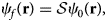
We call the functions  $\hat {\psi }_{{\sf p}}( {\bf r},\; {\boldsymbol \rho })$ the “beamlet” basis due to their similarity to wavelets in the signal processing literature (Mallat, Reference Mallat2009). An example beamlet basis is depicted in Figure 3a in the center panel. These new probe basis functions can be pre-computed and stored in memory, such that only summation over the parent beams is necessary to calculate a diffraction pattern.

Fig. 3. Flow chart of the beam partitioning algorithm for STEM simulation. (a) Calculate the projected potential slices from the atomic coordinates and lookup tables. (b) Partition the probe into the desired number of beams, calculate the basis functions for all beamlets. (c) Perform a multislice simulation of all beams defined by the partitioning, store results in compact  ${\cal S}$-matrix. (d) Construct STEM probes at all positions by multiplying the shifted initial probes by the ${\cal S}$-matrix and then summing over all beams.
Algorithmic Steps of Partitioned PRISM Simulations
Figure 3 shows the steps of our new simulation algorithm as a flow chart. As in all of the above electron scattering simulation methods, the first step is to compute the projected potentials from the atomic coordinates. Figure 3a shows the sum of all 40 projected potential slices, each having a thickness of 2 Å.
The second step, shown in Figure 3b, is to choose a set of parent beams and then calculate the weight function of all beamlets using the desired partitioning scheme. Here, we have used two rings of triangularly tiled beams, where each ring has a constant radius and the beams are separated by 10 mrads across the 20 mrad STEM probe. The beamlet weights w are calculated using natural neighbor interpolation and are shown in Figure 3a in the top right panel. The parent beams are indicated by small red circles in the condenser aperture, and the beamlet weight distributions for each parent beam are show in gray scale. By taking the inverse Fourier transform of each weight function, we can generate the real-space beamlet basis functions  $\hat {\psi }_{{\sf p}}$.
Figure 3c shows the third step of the partitioning simulation algorithm, where we perform a plane-wave multislice simulation for each of the parent beams defined above. After the plane waves have been propagated and transmitted through all 40 slices, the tilt of each beam is removed. These outputs are then stored in the compact  ${\cal S}$-matrix ${\cal S}_{{\bf r}, {\sf p}}$.
Finally, we compute the intensity of each desired STEM probe position as shown in Figure 3d. First, if we are using a PRISM interpolation factor other than f = 1, we crop out a subset of the  ${\cal S}$-matrix. Next, each beam of the ${\cal S}$-matrix is multiplied by the beamlet basis functions, and all beamlet exit waves summed to form the complex STEM probe in real space. Finally, we take the Fourier transform of these probes and compute the intensity from the magnitude squared of the wavefunction. If we require sub-pixel shifts of the STEM probes with the cropped region of the ${\cal S}$-matrix, we must first multiply the probe basis functions by the appropriate complex plane wave in Fourier space to achieve the desired shift. This adds some computational overhead to each probe, and so if possible we suggest using a potential sampling pixel size that produces a simulation image size which is an integer multiple of the spacing between adjacent STEM probes.
Computational and Memory Complexity
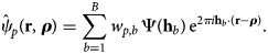
We now approximate computational complexity and memory complexity for the multislice, PRISM, and partitioned PRISM algorithms. We neglect calculation time for the sample-projected potential slice and thermal diffuse scattering, as the added computational and memory complexity is equal for all methods. For simplicity, we assume a quadratic simulation cell with  ${\sf N} = {\sf N}_1 = {\sf N}_2$. Each slice of the multi-slice algorithm requires transmission and propagation operations in equation (8), which is $6{\sf N}^{2} \log _2( {\sf N})$, and $2{\sf N}^{2}$ operations to multiply the potential and the Fresnel propagator. For a STEM simulation with ${\sf P}$ STEM probe positions and ${\sf H}$ slices for the sample, the total multi-slice complexity is then $\Theta ( {\sf H}{\sf P}( 6{\sf N}^{2} \log _2( {\sf N}) + 2{\sf N}^{2})$ (Ophus, Reference Ophus2017). The complexity of the PRISM algorithm is given by $\Theta ( ( {{\sf HB}}/{f^{2}}) [ 6{\sf N}^{2} \log _2( {\sf N}) + 2{\sf N}^{2}] + {{\sf P}{\sf B}{\sf N}^{2}}/{4f^{4}})$ (Ophus, Reference Ophus2017), which consists of ${\sf H}{\sf B}$ multi-slice simulations for each of the sampled beams, and ${{\sf P}{\sf B}{\sf N}^{2}}/{4f^{4}}$ operations for the summation of the beams. For the partitioned PRISM algorithm with ${\sf B}_p$ partitions, the complexity for the multi-slice calculations is $\Theta ( ( {H{\sf B}_p}/{f^{2}}) [ 6{\sf N}^{2} \log _2( {\sf N}) + 2{\sf N}^{2}] )$. For the real-space summation with subpixel precision, a maximum of ${{\sf P} {\sf B} {\sf B}_p {\sf N}^{2}}/{4f^{2}}$ operations is necessary, while for the integer positions on the ${\cal S}$-matrix-grid, only ${{\sf P}{\sf B}_p {\sf N}^{2}}/{4f^{2}}$ operations are necessary.
The memory complexity of the multi-slice algorithm is lowest, since only the current wave of size  $\Theta ( {\sf N}^{2})$ needs to be held in memory for an unparallelized implementation. All algorithms need $\Theta ( {{\sf P}{\sf N}^{2}}/{f^{2}})$ memory to store the results of the calculation if 4D datasets are computed. The PRISM algorithm requires $\Theta ( {{\sf B}{\sf N}^{2}}/{4})$ memory to store the compact ${\cal S}$-matrix. For simulations which require a finely sampled diffraction disk, ${\sf B}$ can quickly grow to 104 or larger, since the number of beams scales with the square of the bright-field disk radius, such that large-scale simulations with fine diffraction disks can outgrow the available memory on many devices. The memory requirements of the partitioned PRISM algorithm scale with $\Theta ( {{\sf B}_p {\sf N}^{2}}/{4})$. Since the number of parent beams ${\sf B}_p$ can be chosen freely, the memory requirements of the partitioned PRISM algorithm can be freely adjusted to the available hardware (Table I).
Table 1. Computational and Memory Complexity of Alternatives for Computing STEM Data.
 ${\sf H}$: number of slices, ${\sf B}$: number of beams, ${\sf B}_p$: number of beam partitions, ${\sf P}$: number of probes, ${\sf N}$: side length of field of view in pixels, f: interpolation factor.
Methods
All the simulations shown in this paper were performed using a set of custom Matlab codes. In addition to implementing the partitioned PRISM algorithm, we have also implemented both the conventional multislice and PRISM algorithms for STEM simulation, in order to make a fair comparison between the different methods. We have used a single frozen phonon configuration in all cases, in order to increase the number of features visible in diffraction space. No effort was made for performance optimization or parallelization beyond MATLAB's inline compiler optimizations.
The microscope parameters used in Figures 4, 5, and 6 were an accelerating voltage of 80 kV, a probe convergence semiangle of 20 mrad, and a pixel size of 0.1 Å. The probe was set to zero defocus at the entrance surface of the simulation cell. The projected potentials were calculated using a 3D lookup table method (Rangel DaCosta et al., Reference Rangel DaCosta, Brown and Ophus2021) using the parameterized atomic potentials given in Kirkland (Reference Kirkland2020). Slice thicknesses of 2 Å were used for all simulations, and an anti-aliasing aperture was used to zero the pixel intensities at spatial frequencies above 0.5 · q max during the propagation step.
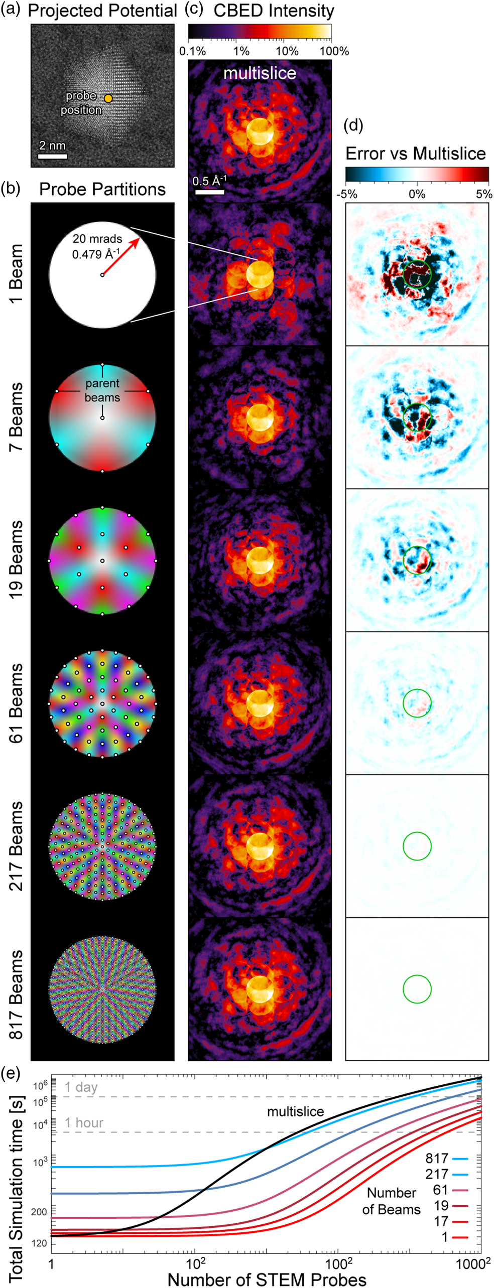
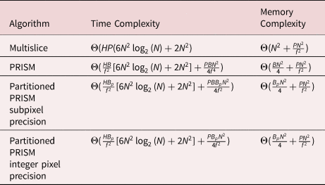
Fig. 4. Individual STEM probes computed with beam partitioning. (a) Projected potential and probe position. (b) Partitioning diagram showing beamlet weights. (c) Calculated CBED intensity on a logarithmic scale. (d) Error versus multislice probe simulation. (e) Estimated calculation time of the different probe partitions as a function of the number of probes calculated.
Fig. 5. Individual STEM probes computed with beam partitioning and PRISM f = 5 interpolation. (a) Projected potential and probe position. (b) Partitioning diagram showing beamlet weights. (c) Calculated CBED intensity on a logarithmic scale. (d) Error versus multislice probe simulation. (e) Estimated calculation time of the different probe partitions as a function of the number of probes calculated.
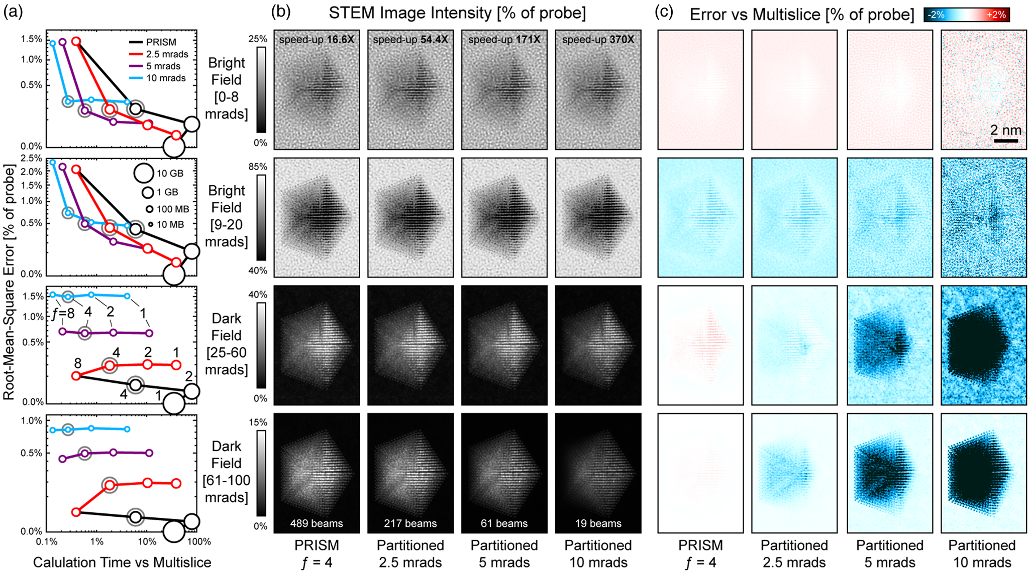
Fig. 6. Simulation of STEM images using beam partitioning and PRISM interpolation. (a) Calculation time, RMS error relative to multislice, and total RAM required for the  ${\cal S}$-matrix of all simulations. The four detector configurations considered are BF detector from 0 to 8 mrads, an ABF detector from 9 to 20 mrads, a LAADF detector from 25 to 60 mrads, and a HAADF detector from 61 to 100 mrads. Gray circles indicate the simulations where images are shown. (b) STEM images for the four detector configurations and four simulation cases labeled below. Calculation of time speed-up-relative multislice is inset into the top row, while the number of included beams is inset into the bottom row. (c) Pixel-wise errors of each image in (b) with respect to multislice simulations.
The atomic coordinates utilized for our single probe position and imaging simulations are identical to that used previously (Ophus, Reference Ophus2017). The structure consists of a Pt nanoparticle with a multiply-twinned decahedral structure, with screw and edge dislocations present in two of the grains. The nanoparticle measures approximately 7 nm in diameter and was tilted such that two of the platinum grains are aligned to a low index zone axis. It was embedded into an amorphous carbon support to a depth of approximately 1 nm, with all overlapping carbon atoms removed. The cell size is 10 nm × 10 nm × 8 nm and contains 57,443 total atoms. The nanoparticle coordinates were taken from Chen et al. (Reference Chen, Zhu, White, Chiu, Scott, Regan, Marks, Huang and Miao2013), and the amorphous carbon structure was adapted from Ricolleau et al. (Reference Ricolleau, Le Bouar, Amara, Landon-Cardinal and Alloyeau2013).
The atomic coordinates of our 4D-STEM simulations were a multilayer stack of semiconductor materials inspired by the experiments from Ozdol et al. (Reference Ozdol, Gammer, Jin, Ercius, Ophus, Ciston and Minor2015). The simulation cell consists of a GaAs substrate where the Ga and As sites are randomly replaced with 10% Al and P, respectively. The multilayers are an alternating stack of GaAs doped with 10% P and pure GaAs, respectively, each 9 unit cells thick along a [001] direction. The lattice parameters of the GaAs and GaAsP were fixed to be +1.5 and −1.5% of the substrate lattice parameter, which was set to 5.569 Å. The field of view was approximately 500 × 500 Å, and the potential pixel size and slice thicknesses were set to 0.1 and 2 Å, respectively. The cell thickness was approximately 40 Å, giving 4.6 million atoms inside the simulated volume. The STEM probe convergence semiangle was set to 2.2 mrads, the accelerating voltage was set to 300 kV, and the probe was scanned over the field of view with 2 Å step sizes, giving an output of 250 × 250 probes.
The simulations shown in Figures 4, 5, and 7 were computed on a laptop with an Intel Core i7-10875H CPU, operating at 2.30 GHz with eight cores, and 64 GB of DDR4 RAM operating at 2,933 MHz. The simulations shown in Figure 6 were performed on Intel Xeon Processors E5-2698v3 with eight Physical cores (16 threads) and 25GB RAM per simulation. The multislice 512 × 512 results were obtained by splitting the 512 × 512 array into 32 jobs with 16 × 512 positions. Prism f = 2 results with 512 × 512 probe positions were obtained by splitting the array in to eight jobs with 64 × 512 each, all using an identical calculated  ${\cal S}$-matrix. All calculations were performed using Matlab's single floating point complex numbers, and simulation run times were estimated using built-in MATLAB functions, and memory usages were based on theoretical calculations.
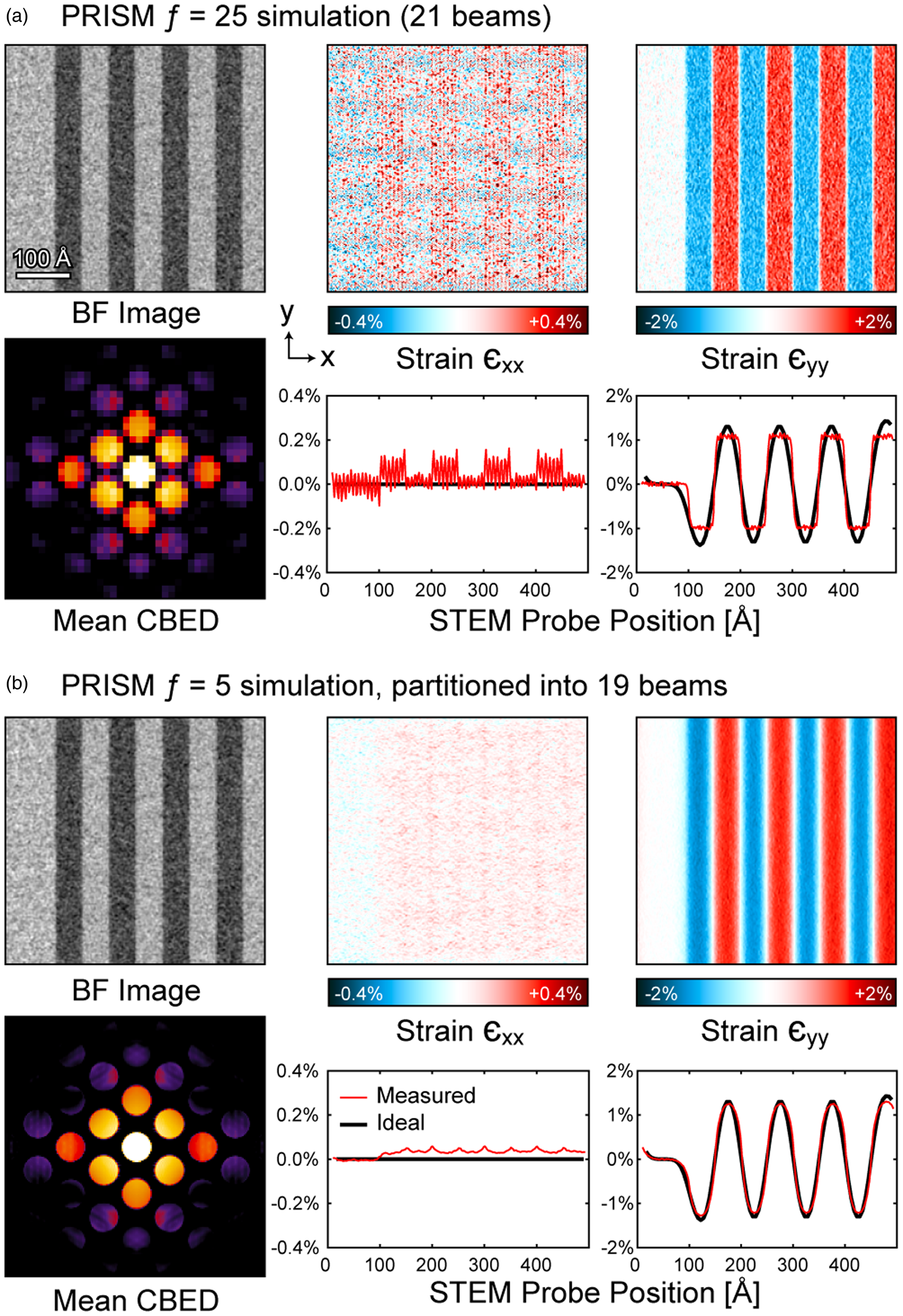
Fig. 7. Simulated 4D-STEM datasets and strain maps of a multilayer semiconductor stack. (a) PRISM simulation with f = 25 interpolation and 21 total beams. (b) Partitioned PRISM simulation with f = 5 interpolation and 19 total beams. Each simulation shows a virtual bright field image, the mean CBED image, and strain maps in the two cardinal directions. Line traces show average strain perpendicular to the layer direction.
Results and Discussion
Calculation of Individual STEM Probes
To demonstrate the accuracy of our proposed algorithm, we have performed STEM simulations of a common sample geometry: a multiply-twinned Pt nanoparticle resting on an amorphous surface. The total projected potential of this sample is plotted in Figure 4a, as well as the location of a STEM probe positioned just off-center. We have tested a series of beam partitioning schemes, shown graphically in Figure 4b. The first case tested was a single beam, which is equivalent to convolving a plane-wave HRTEM simulation with the STEM probe. We have also used natural neighbor partitioning to calculate the beamlet weights when using a series of concentric hexagonal rings of beams, distorted slightly to the circular probe geometry. These simulations include partitioning the 20 mrad probe by 20, 10, 5, 2.5, and 1.25 mrads, resulting in a total of 7, 19, 61, 217,and 817 parent beams, respectively.
The calculated diffraction space intensities of the probes corresponding to the above cases are shown in Figure 4c, along with the corresponding conventional multislice simulation. We see that using a single parent beam is extremely inaccurate, reproducing only the coarsest features of the multislice simulation. However, the partitioning scheme rapidly converges to the multislice result, shown by the error images plotted in Figure 4d. The 19 beam case has errors falling roughly within 5%, while the 61 beam case drops to <2%. The calculated probe for the 217 beam case has errors on the order of <0.5%, which would likely be indistinguishable from an identical experiment due to measurement noise. Finally, the 817 beam case is essentially error-free.
We can make additional observations about the character of the errors present in the partitioning algorithm. Inside the initial probe disk and in directly adjacent regions, the errors are roughly equally distributed in the positive and negative directions. However, at higher angles, the errors are biased in the negative direction. This indicates that the partitioning approximation is highly accurate at low-scattering angles where coherent diffraction dominates the signal, and is less accurate at high-scattering angles where thermal diffuse scattering dominates. We attribute this effect to the complex phase distribution of the pixels; at low-scattering angles, adjacent beams have very similar phase distributions, which in turn makes the interpolation a good approximation. However, at high-scattering angles, the phases of each pixel are substantially more random, due to thermal motion of the atoms. This means that if too few beams are used to approximate the signal, the coherent summations will tend towards zero due to the random phase factors. Thus, when using a small number of beams in partitioned STEM simulations, high-angle-scattering intensities can be underestimated. In the example diffraction pattern shown in Figure 4d, we also observe that the error magnitude decays from low to high angles when very few beamlets are used, but becomes more uniform when the approximation approaches the fully sampled  ${\cal S}$-matrix. We expect the error distribution to vary with the complexity of the simulated specimen and recommend testing the approximation at few selected positions with high values of projected potential.
The estimated calculation times for these simulations are shown in Figure 4e. When calculating a single STEM probe, multislice is always fastest because the only overhead to the calculation is computation of the projected potentials. The partitioned simulations by contrast require evaluation of the  ${\cal S}$-matrix, which requires the same calculation time as each STEM probe multislice propagation for each beam. However, once the ${\cal S}$-matrix has been computed, the calculation of STEM probes via matrix multiplication becomes substantially faster than multislice. The overall simulation time becomes lower than multislice if many STEM probe positions must be calculated. For the 61, 217, and 817 beam cases, these crossovers in calculation time occur for 32, 135, and 1,000 probe positions, respectively. Therefore, even for 1D simulations of STEM probe positions, the partitioning scheme is faster, and for simulations with a grid of 2D probe position this scheme is significantly faster than multislice.
However, using the beam partitioning algorithm on the entire field of view does not utilize the algorithm to its full speed-up potential. The beam partitioning approximation is also compatible with the PRISM approximation. Partitioning reduces the number of entries of the  ${\cal S}$-matrix in diffraction space, whereas PRISM reduces the number of entries using cropping in real space. Figure 5a shows STEM simulations that combine partitioning with a PRISM interpolation factor of f = 5. The 25-fold reduction in sampling of the STEM probes is evident in Figure 5b, where the underlying beam pixels are clearly visible in the STEM probe. The partitioning scheme used is identical to that of Figure 5b, except for the 1.25 and 2.5 mrad partitioning cases. For the 1.25 mrad partitioning, the number of parent beams outnumbers the number of available beams; after removing duplicate beams, this simulation becomes equivalent to a PRISM f = 5 simulation. The 2.5 mrad partitions were changed to a diagonal grid, where every other beam is included in order to produce a more uniform sampling of the ${\cal S}$-matrix.
The calculated probe intensities are shown in Figure 5c, along with the corresponding multislice simulation (which was sampled on the same 25-fold reduced grid). The errors of the partitioned PRISM simulations have been compared with the multislice simulation in Figure 5d. The resulting convergence towards zero error is essentially identical to the non-PRISM case (where f = 1). These simulations are also slightly biased towards negative errors at high-scattering angles.
The estimated calculation times are plotted in Figure 5e as a function of the number of probe positions. These simulations are substantially faster than multislice. The 61, 161, and 325 beam cases have a crossover in the calculation with multislice for 32, 83, and 155 probe positions, respectively. If the error for the 161 beam case is within an acceptable tolerance, a 1,000 × 1,000 probe position simulation of this sample can be performed in roughly 50 min, without additional parallelization or utilization of GPU or HPC resources.
Calculation of Full STEM Images
We have also simulated full STEM images with a variety of standard detector configurations, in order to demonstrate the potential of the partitioned PRISM algorithm. These simulations are shown in Figure 6 and include four radially symmetric detector configurations. These are a bright-field (BF) image from 0 to 8 mrads, an annular bright-field (ABF) image from 9 to 20 mrads, a low-angle annular dark field (LAADF) image from 25 to 60 mrads, and a high-angle annular dark field (HAADF) image from 60 to 100 mrads. We have performed these simulations with 512 × 512 probe positions using multislice, PRISM, and partitioned PRISM algorithms. The PRISM simulations used interpolation factors of f = 1, 2, 4, and 8, giving a total number of beams equal to 7,377, 1,885, 489, and 137 beams, respectively. The partitioning included was the scheme described above, where the 20 mrad STEM probe was subdivided by 10, 5, and 2.5 mrads into the parent beams, and where no partitioning was performed (i.e. the original PRISM algorithm). The number of beams for the 10, 5, and 2.5 mrad partitioning was equal to 19, 61, and 217 respectively, except for the 2.5 mrad partitioning for f = 8 interpolation, where the simulation is equivalent to PRISM (137 beams).
Figure 6a shows a summary of the results, where the root-mean-square (RMS) errors in units of probe intensity and calculation times relative to multislice simulations are plotted. Additionally, the RAM requirements for storing the  ${\cal S}$-matrix are shown by the marker sizes. Overall, the results follow the same trend as in the previous section. Using less beams either in the partitioning or higher PRISM interpolation results in a less accurate simulation for all cases. The only exception to this is PRISM f = 1 simulations, which are mathematically identical to multislice simulations (Ophus, Reference Ophus2017). Interestingly, the PRISM f = 1 simulations are faster than f = 2, due to not needing any matrix indexing operations to crop out a portion of the ${\cal S}$-matrix. However, f = 1 PRISM simulations also have the largest RAM requirements by a large margin, requiring 15.5 GB. This is potentially an issue for large simulations if we wish to utilize GPU resources, since RAM capacities of current GPUs are often in the range of 4–16 GB, and there is additional overhead for other arrays that must be calculated. This problem can be alleviated by streaming only part of the ${\cal S}$-matrix into the GPU RAM (Pryor et al., Reference Pryor, Ophus and Miao2017), but then the large speed-up afforded by performing only a single matrix multiplication per STEM probe is lost.
The BF and ABF simulation errors are shown in Figure 6a, and the partitioned simulations have a very favourable balance between calculation time and accuracy. For PRISM interpolation factors of f = 2 and f = 4, the partitioned simulations have essentially identical accuracy to the PRISM simulations, while requiring far lower calculation times and less RAM to store the  ${\cal S}$-matrix. The 5 mrad partitioning case (61 beams), for example, is 46 (f = 2) and 171 (f = 4) times faster than an equivalent multislice simulation, while having RMS errors on the order of 0.2 and 0.1%, respectively, for the 0–8 mrads BF image and RMS errors on order of 0.5 and 0.2%, respectively, for the 9–20 mrads ABF image.
For the LAADF and HAADF images shown in Figure 6a, the partitioned simulations show somewhat less favourable error scaling than the PRISM algorithm. While the calculation times are reduced by partitioning for a given PRISM interpolation factor, the errors increase roughly inversely proportional to the number of include beams. These errors are still relatively low however, staying roughly constant with the interpolation factor f.
Figure 6b shows the STEM images for the f = 4 cases including conventional PRISM and the 3 partitioning schemes. It is immediately evident that all images contain the same qualitative information, for example, showing that the ABF image is far more interpretable than the BF image. Visually, the BF and ABF images appear indistinguishable from each other, with all atomic-scale features preserved across the different partitioning schemes. The LAADF and HAADF images similarly all contain the same qualitative information, and all highlight the differences between these two dark-field imaging conditions. Here, however, we can see an overall reduction of image intensity inside the nanoparticle for the partitioned simulations with less beams. In the LAADF case, the 19 beam image is noticeably dimmer than the other cases, and for the HAADF case both the 19 and 61 beam partitioning show reduced intensities.
To show the errors more quantitatively as a function of the probe position, we have plotted the difference images with respect to a multislice simulation in Figure 6c. For the BF images, a slight offset in the overall intensities is visible, likely due to the slightly different probe and detector sampling when using f = 4 interpolation. The spatially resolved differences are very low however, for both PRISM and the 2.5 and 5 mrad partitioning simulations. In the regions of highest scattering in the nanoparticle, some errors along the atomic planes are visible in the 10 mrad partitioned simulation. The 2.5 and 5 mrads partitioned PRISM simulations are an excellent replacement for the PRISM simulations, as they offer large calculation time speed-ups for a negligible change in the error.
In the LAADF and HAADF error images plotted in Figure 6c, the errors are increasing proportionally to the inverse of the number of beams included, as we observed in Figure 6a. The HAADF images show higher overall errors than the LAADF images due to the increasing randomness of the pixel phases at high-scattering angles where thermal diffuse scattering dominates the signal. The relative error is also higher at these high-scattering angles, as the number of electrons that scatter to these high angles are significantly lower than those which reach the other detector configurations. Both the LAADF and HAADF errors scale nearly linearly with the nanoparticle projected potential, which indicate that they may be tolerable for relative measurements such as comparing different thicknesses or the signal measured for different atomic species. For quantitative intensity simulations at high angles, we recommend using as many beams as possible for the partitioned PRISM algorithm.
Calculation of 4D-STEM Datasets
Many 4D-STEM experimental methods require fine enough sampling of reciprocal space to resolve the edges of scattered Bragg disks, or fine details inside the unscattered and scattered Bragg disks (Ophus, Reference Ophus2019). In particular, for machine learning methods which are trained on simulated data, we want the sampling and image sizes to be as close to the experimental parameters as possible (Xu & LeBeau, Reference Xu and LeBeau2018; Yuan et al., Reference Yuan, Zhang, He and Zuo2021). Here, compare the PRISM and partitioned PRISM algorithms for 4D-STEM simulations and assess their accuracy by performing a common 4D-STEM workflow of strain mapping by measuring the Bragg disk spacing (Pekin et al., Reference Pekin, Gammer, Ciston, Minor and Ophus2017).
We have simulated a 4D-STEM experiment for a multilayer stack of semiconductor materials similar to the experiments performed by Ozdol et al. (Reference Ozdol, Gammer, Jin, Ercius, Ophus, Ciston and Minor2015), as shown in Figure 7 and described above. Two simulations were performed: the first used only the PRISM algorithm with interpolation factors of f = 25, giving 21 total beams, as shown in Figure 7a. The second combined a PRISM interpolation of f = 5 with partitioning into 19 beams, as shown in Figure 7b. These parameters were chosen to require approximately the same total calculation time (157 and 186 min for pure PRISM and partitioned PRISM, respectively). Both simulations used the same atomic potentials which required 113 min to compute. The  ${\cal S}$-matrix calculation steps required 42 and 30 min for the pure PRISM and partitioned PRISM simulations, respectively. Finally, the 62,500 probe positions required 2 and 43 min for the pure PRISM and partitioned PRISM simulations, respectively.
We have used the py4DSTEM package published by Savitzky et al. (Reference Savitzky, Hughes, Zeltmann, Brown, Zhao, Pelz, Barnard, Donohue, DaCosta, Pekin, Kennedy, Janish, Schneider, Herring, Gopal, Anapolsky, Ercius, Scott, Ciston, Minor and Ophus2020) to measure strain in both of the simulations, as shown in Figure 7, by fitting the positions of the Bragg disks. These strains are compared to the ideal strain, estimated by convolving the underlying lattice spacing with a Gaussian kernel with a standard deviation given by the 5 Å estimated size of the STEM probe. In the pure PRISM simulation shown in Figure 7a, there are artifacts visible in both strain maps. The strain perpendicular to the layer direction shows rapid oscillations of ±0.1%, while the strain parallel to the layer direction shows discrete steps. Both of these are due to the very small cropping box used when f = 25, which cuts off the tails of the STEM probe in this simulation. Additionally, the limited sampling of the diffraction disk edges strongly limits the achievable precision in the disk position measurements.
By contrast, the partitioned simulation shown in Figure 7b samples diffraction space five times more finely in both the x and y directions. The resulting strain maps are much flatter, and the measured strain positions agree better with the ideal measurements. This simulation demonstrates that beam partitioning combined with PRISM interpolation can provide a much more efficient use of the calculation time required to generate the  ${\cal S}$-matrix beams than a pure PRISM simulation. This partitioning case uses approximately the same number of beams and requires roughly the same calculation time, but is substantially more accurate at the low-scattering angles used in a coherent diffraction 4D-STEM simulation. We also estimate that a multislice simulation of this same experiment would require approximately 60 days using the same simulation parameters. Even if we were to increase the beam sampling by a factor of 8, the partitioned PRISM simulation would still complete in less than a day.
Conclusion
We have introduced the beam partitioning algorithm for STEM simulation. This algorithm splits the STEM probe into a series of basis functions generated by natural neighbor interpolation between a set of parent beams. We construct the diffracted STEM probe by matrix multiplication of these basis functions with plane-wave multislice simulations of each parent beam which are stored in a  ${\cal S}$-matrix that can be re-used for each new STEM probe position. We have demonstrated that the resulting algorithm converges rapidly to low error with respect to the conventional multislice algorithm, and that it is fully compatible with the PRISM algorithm for STEM simulation.
We have compared our new algorithm with multislice and PRISM simulations of a nanoparticle on an amorphous substrate. With these simulations, we have shown that in general, partitioned beam simulations can provide the same accuracy as PRISM at low- to intermediate-scattering angles (where coherent diffraction dominates the signal), but with much lower calculation times and lower RAM usage. We have also shown that at high-scattering angles, beam partitioning simulation accuracy is somewhat worse than the PRISM algorithm, though still with lower calculation times. These low calculation times may allow the partitioned PRISM algorithm to be used “in the loop” with 3D tomographic reconstruction algorithms, in order to properly model the nonlinear dependence of STEM image contrast on the underlying atomic potentials.
Finally, we have also demonstrated the utility of partitioned PRISM for simulations of large 4D-STEM datasets. We used a common sample geometry composed of a multilayer stack of semiconductor materials with varying compositions on a substrate and performed strain mapping from the diffracted probe signals by measuring the position of the Bragg disks and fitting a lattice. These simulations show that the partitioned PRISM algorithm is particularly well suited for performing fast simulations of large fields of view where high sampling of diffraction space is needed. We believe that our algorithm will find widespread application in simulations of very large simulated cells, such as those calculated with molecular dynamics. Our simulations also show that the beam partitioning  ${\cal S}$-matrix can efficiently represent complex three-dimensional scattering, which may make it useful for inverting experimental data efficiently.
Availability of data and materials
Reference implementations of the algorithms presented in this paper (multislice, PRISM, and partitioned beam STEM simulations) are available at https://github.com/cophus/superPRISM.
Acknowledgments
We thank Hamish Brown and Scott Findlay for useful discussions. Philipp M. Pelz and Mary C. Scott are supported by the Strobe STC Research Center (Grant No. DMR 1548924). Luis Rangel Dacosta and Benjamin H. Savitzky are supported by the Toyota Research Institute; Luis Rangel Dacosta is also supported by the Department of Energy Computational Science Graduate Fellowship. Colin Ophus acknowledges support from the Department of Energy Early Career Research Award program. Work at the Molecular Foundry was supported by the Office of Science, Office of Basic Energy Sciences, of the U.S. Department of Energy under Contract No. DE-AC02-05CH11231. This research used resources of the National Energy Research Scientific Computing Center (NERSC), a U.S. Department of Energy Office of Science User Facility located at Lawrence Berkeley National Laboratory, operated under Contract No. DE-AC02-05CH11231. This material is based upon work supported by the U.S. Department of Energy, Office of Science, Office of Advanced Scientific Computing Research, Department of Energy Computational Science Graduate Fellowship under Award Number DE-SC0021110.


 Open access