


Introduction
The field of nanotechnology has diversified into different areas of research, from materials science to biotechnology. Many of these applications are based on the ability to fabricate or manipulate nanostructured materials [Reference Pinilla-Cienfuegos1]. One convenient technique for structuring, manipulation, and fabrication at the nanometer scale is atomic force microscopy (AFM) nanolithography. All AFM nanolithography techniques can be classified into two general groups in terms of their operational principles: force-assisted nanolithography and bias-assisted nanolithography [Reference Pineda2]. The force-assisted method consists of applying a large force to a sharp tip to mechanically modify the surface atoms or molecules of the sample and produce trenches on the surface. In this case, the interaction between the tip and the sample is purely mechanical [Reference Pineda2]. On the contrary, the bias-assisted method entails applying a voltage between the AFM tip and the substrate in contact with the sample. The tip-sample voltage induces an electrochemical reaction that produces oxide on the surface of the substrate [Reference Pinilla-Cienfuegos1].
This article demonstrates an electrochemical process called anodic oxidation using the bias-assisted lithography method to create oxide patterns on the surface of a silicon substrate. The success of this technique relies on using the AFM tip as a biased cathode to the sample surface. Also, the water meniscus around the sample acts as an electrolyte for the chemical reaction. The environment humidity directly influences the size of the meniscus [Reference Pinilla-Cienfuegos1]. Below we report nanoscale oxide line formation using AFM anodized lithography.
Materials and Methods
For this experiment, a Park NX10 AFM was used to perform bias-assisted nanolithography to draw nanopatterns onto a bare silicon substrate. The oxide patterns were formed using Park SmartLitho™ software [3]. Non-contact mode imaging was conducted after the lithography process to confirm the successful fabrication of the oxide patterns on the surface as well as to distinguish the surface difference between the oxide layers and silicon substrate. A conductive AFM cantilever probe (Multi 75G) with a nominal spring constant (k = 3 N/m) and resonance frequency (f = 75 kHz) was used in these experiments.
The Park SmartLitho software consists of five windows and panels that allow the operator to control the complete lithography process (Figure 1). In the first step, the appropriate alignment of the super-luminescent diode (SLD) and position-sensitive photodetector (PSPD) is verified (Figure 1A). After confirming the correct alignment, the operator selects the control mode; in this case, the setpoint mode was selected. For the anodic oxidation, a bias has to be applied; in this case, the tip was chosen as the desired channel (Figure 1B). In the design area (Figure 1C), the operator can insert the desired figures and shapes using a previous AFM image as a baseline. All embedded figures appear in the object list (in this case, just one line) (Figure 1D). The operator can change the formation order, and the estimated lithography time for each figure is provided. Finally, for any desired feature, parameters can be changed in the object edit panel (Figure 1E). Parameters such as voltage, load force, stroke speed, extend speed, or lift speed can be modified to obtain different features within the same designed figures.

Figure 1: Park SmartLitho™ software: A) Vision and monitoring view; B) Nanolithography mode panel; C) Lithography design area; D) Objects list; E) Objects edit panel.
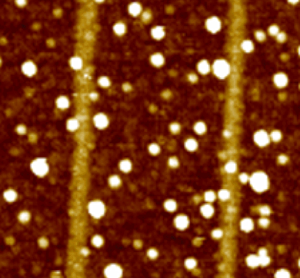
To start a lithography or manipulation process, a baseline image is needed. In this case, the baseline image already contains one previously drawn line to compare with the line about to be drawn (Figure 1C). The image is 1.5 µm by 1.5 µm. The sample features small nanoparticles on its surface, according to the image taken using non-contact AFM mode.
The lithography process is planned by drawing a shape on the surface using the software. The AFM operating software, Park SmartScan™, provides the operator with offset and easy positioning features. The DC bias lithography process is done in contact mode, and in this case, a bias of negative 5.0 volts is applied between the tip and sample. For this experiment, a line was drawn at 0.2 µm/s with a 200 nN load force. The drawn line is approximately 1.8 µm in length (Figure 2, top left). The process takes a couple of seconds to complete. As the cantilever is compressed to the loading force of 200 nN, the PSPD signal moves up, which visually verifies the applied pressure.

Figure 2: Nanolithography process: (top left) Post-scan image; (top right) 3D view; (bottom) Line profile plotted of green line seen in top left.
Results and Discussion
Following the lithography process and using Park SmartScan, the system is switched back to non-contact mode. An AFM cantilever probe is mounted on a piezoelectric bimorph shaker, attached to the AFM head Z piezoelectric scanner. The shaker vibrates the AFM cantilever probe at its resonant frequency, which is automatically selected along with the vibration amplitude. As the probe nears the sample surface, the vibration amplitude decreases. Likewise, as the probe moves away from the surface, the amplitude increases. The Z piezo scanner moves up and down and adjusts its height to maintain a constant vibration amplitude. The height adjustment of the scanner thus reflects the height change on the sample surface. The AFM raster scans and detects the height change point-by-point in the XY-direction to map out the three-dimensional surface topography. The tip approaches the surface, and the image is retaken promptly with the same parameters as the baseline AFM image. The newly drawn line is clearly visible and parallel to the previously drawn line (Figure 2, top left). Note that the image position remains the same, showing the control of the XY-scanner, separate from the Z-scanner, even at smaller scan sizes. In this example, the lithography process is done in contact mode, and, therefore, imaging in non-contact mode is an option. However, after the manipulation, it is important to take the image using non-contact mode to avoid disturbing the particles present on the sample.
After verifying success of the lithography process, the final image is taken and exported to the analysis software called Park XEI™ [4]. In this case, we can see that the previously drawn line is around 35 nm in width, and the newly drawn one is 47 nm (Figure 2, bottom). Both lines are drawn using the same lithography parameters. Nevertheless, the line on the right side, drawn first, is observed to be narrower than the oxide line on the left. This might be due to performing the lithography in contact mode. In contact mode, the tip is rubbed against the sample surface as the lines are drawn. The rubbing can cause the end of the tip to wear out and blunt. The blunted tip can fabricate wider oxide lines than the ones drawn with a sharper tip [Reference Pinilla-Cienfuegos1,Reference Voves5].
We can see that the resulting line-height is approximately 1.4 nm for both lines when adding another cursor. Park XEI software is capable of showing a three-dimensional rendering of the image taken (Figure 2, top right). With the 3D representation, we note that the lines drawn during this oxide growth process have a lower height than the nanoparticles on the surface.
Conclusion
This article discusses the use of Park SmartLitho™ software to design and customize nanoscale oxide patterns using a Park NX10 AFM. With only a few seconds of runtime, this simple test case demonstrates a bias-assisted nanolithography process, which successfully generates oxide patterns as narrow as 35 nm in width. Although the process itself employs contact mode, true non-contact mode before and after the operation validates that the new oxide line is indeed parallel to the line in the baseline image. This test case also demonstrates the scanning and imaging precision of Park's XY-scanner. Overall, this study shows that the bias mode in the SmartLitho software is an excellent tool for generating well-defined nanoscale patterns and features.


