


Introduction
Scanning electron microscopes (SEMs) are often considered to be one of the most versatile and powerful tools for scientists and researchers. These instruments provide a large depth of field relative to optical microscopes at high spatial resolution, and they integrate the ability to analyze the chemical composition of materials in situ via several types of spectroscopy.
SEMs deliver a high degree of analytical capability, including revealing surface structure and chemistry at nanoscale resolution. This permits, among other capabilities, easy visualization of specimen topography and microstructure, or establishing the cause of quality control problems, in some cases through a single image.
Historically, however, SEMs have been limited to large laboratories with the budget and infrastructure to support the installation of full-scale SEMs. The creation of compact SEM instruments, designed to fit on a benchtop without the need for any specialized facilities, have transformed that landscape and the onset of new technologies. Benchtop systems are designed with ease of use in mind, allowing users of any experience level to acquire robust data without the need for highly specialized and time-consuming training. They also come at an attractive price point and are suitable for a wide range of applications from industry (quality control, manufacturing, R&D) to science education and academia.
Combining the resolution of an electron microscope with the ease-of-use function of an optical microscope, benchtop instruments are revolutionizing the idea of SEMs. This article discusses the usage of benchtop SEMs for research in a wide range of applications, including materials science, pharmaceuticals, energy, academia, and science education.
Materials Science
Within materials science, efficient visual and chemical characterization of materials is essential for production and quality control. This may include the identification of foreign substances, forensic examinations and quality control in additive manufacturing, and automotive/aerospace cleanliness. As manmade materials evolve from the macro- to the micro-, nano-, and even pico-scale, the demand for higher-resolution microscopy techniques has increased.
One research area in which SEMs stand out is particle analysis (Figure 1). In order to elucidate questions surrounding particle size, morphology, surface area, and porosity, researchers have traditionally turned to light scattering, light obscuration, or direct imaging techniques. SEMs offer the ability to rapidly collect this data as well as chemical information, providing additional valuable insight into materials characterization without sacrificing significant time or resources. For decades, microscopy has been a failure analyst's most powerful tool in determining the causes of failure in a wide variety of materials. With growing material complexity, manufacturers need fast, reliable, and scalable quality control processes.

Figure 1: Secondary electron image of tin alloy particle showing variations in surface morphology and grain size. Imaged via JEOL JCM-7000 Benchtop SEM.
Scanning electron microscopy is well-suited to perform particle and fiber analysis by providing a high-resolution view of the sample's surface morphology and details on sizes and shapes. Benchtop SEM users can quickly reproduce operating conditions by the click of a button to easily compare sample data to standards, making it straightforward to repeat tests within a set of parameters.
The combination of a benchtop SEM with energy-dispersive X-ray spectroscopy (EDS) is the ideal solution for integrating particle visualization and chemical composition analysis. In quality control, for example, such a combination helps to determine the thickness of coatings, assess the size and composition distribution of particles, and identify grain boundaries. These types of analyses are often critical initial steps in materials characterization workflows applicable to a range of materials science fields. The benchtop SEM is a quick, cost-effective, and robust option for streamlining this workflow. This SEM/EDS resource performs full morphologic and chemical characterization of specimens, offering a high level of performance in terms of resolution, complimentary analytical detectors, and intuitive integrated software for comprehensive analysis.
Pharmaceutical Research and Development
Pharmaceutical research and development focuses on the advancement of new drugs and the improvement of existing drugs. With new pathogens continually evolving and the ever-growing resistance to existing drugs, the pharmaceutical industry is facing a significant challenge.
All solid pharmaceutical products contain an active pharmaceutical ingredient (API), along with a mixture of excipients (bulking agents, stabilizers, and coatings), resulting in the final product. These formulations must be optimized morphologically and chemically, since factors such as homogeneity, texture, and particle size may affect the shelf life, dosage, and effective release of drugs. The mechanical properties of APIs and excipients in solid products determine how their blends behave during tableting, milling, and coating.
Pharmaceuticals are designed at the nanoscale, enabling drugs to interact with cellular structures and improve their delivery to desired locations in the body. Correspondingly, these nanoscale designs require measurement, analysis, and imaging capabilities at the nanometer scale. Unprecedented demand, along with the growing complexity of new therapeutics, means research and analysis techniques must be able to support the development of novel and more powerful drugs and drug delivery techniques to treat diseases.
Benchtop SEMs play an important role in controlling particle sizes and excipient selection. They also help to characterize the tablet coating thickness, pore structure, roughness, and surface area of coating materials. SEM imaging can be used in manufacturing processes such as quality control to make sure each batch of excipients or APIs is consistent. In addition, once a solid pharmaceutical product is formulated, SEMs can be used to evaluate how well the ingredients blend together. With an integrated EDS detector, a benchtop SEM may reveal detailed chemical zoning, that is, the types and amounts of elements and their spatial distribution (Figure 2).

Figure 2: Backscattered electron image and EDS map of a pharmaceutical API for drug delivery, highlighting chemical heterogeneity within the tablet. Lansoprazole, used for heartburn relief. Imaged via JEOL JCM-7000 Benchtop SEM.
A benchtop SEM has a smaller footprint and a lower operation cost than a traditional SEM, making it straightforward to integrate into a laboratory's workflow. With a benchtop SEM, pharmaceutical companies gain a robust and versatile tool for analyzing substance morphology, topography, and composition right from their own laboratory environment.
Energy Exploration
The search for sustainable energy sources is prompting the development of technologies capable of tapping into solar, wind, geothermal, and tidal energy. To fully take advantage of these power sources, engineers need new ways of storing and converting these energies. Within research and development, battery technology is currently a major focus. Batteries serve as the power source of choice for portable electronic devices, including smartphones, smart watches, and laptops, as well as the increasingly popular electric vehicle. They are complex energy storage devices with unique electrochemical characteristics, combining high-density metals, low-density polymers, and other materials.
The interfacial region of battery technologies has constantly presented new challenges for analysts in the quest to improve their quality, safety, and lifespan. Batteries often contain multiple thin films that are synthesized to form solid−solid interfaces. These interfaces consist of thin layers of cathode material, insulating barriers, anode materials, metal current collectors, and the electrolyte. The form of these materials can be powders, sheets, and fluids, which require assessment before and after assembly, and after repeated charge/discharge operations.
Benchtop SEMs have been used to analyze the interfacial regions such as the surfaces of cathodes and anodes (Figure 3). They allow for visualization of the material interface, particle size, distribution, and void spaces. This information can lead to improvement in performance and longevity by guiding the design of electrode materials with adequate energy density and efficiently designed electrode and electrolyte configurations.

Figure 3: Backscattered electron image and EDS map of cross-sectioned battery layers showing variations in morphology, thickness, and chemistry between the layers. Imaged via JEOL JCM-7000 Benchtop SEM.
SEMs support the development of new battery technologies with morphological observation at the micrometer to nanometer scale, as well as the chemical analysis needed to create high-performance coatings and powders. SEMs allow direct imaging and analysis of these battery constituents with nanometer resolution.
Additionally, scanning electron microscopy is a major analytical platform for studying the mechanical, chemical, and structural properties in electronic components (Figure 4). Using a benchtop SEM, engineers can distinguish the structure and properties of components in semiconductor chip packaged design, as well as the individual electronic components. Benchtop SEM technology can be used during component manufacturing to ensure quality control as well as post-manufacturing for failure analysis.
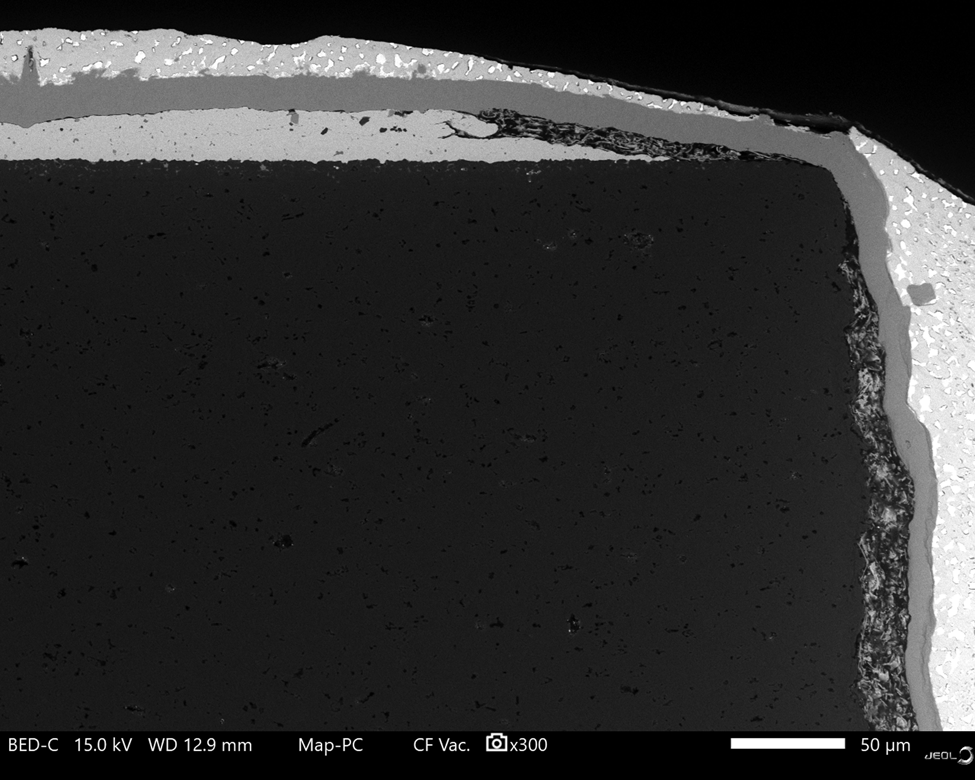
Figure 4: Backscattered electron image of a capacitor cross section showing variations in layer thickness and morphology as well as composition. Imaged via JEOL JCM-7000 Benchtop SEM.
Science Education and Academia
Benchtop SEMs are not only transforming industry spaces but are also playing an invaluable role in academic research and science education. SEM instruments have long been critical research infrastructure within the academic sector across a broad range of topics, from biology to geology to engineering. However, the high cost of ownership and need for specialized users can be a barrier to entry for smaller academic institutions. Now more than ever, with both industry and academic SEM applications skyrocketing, giving students access to SEMs within the classroom and laboratory provides important and transferable skills for their future careers. The benchtop SEM reduces these barriers: integrated software paired with low cost of ownership and maintenance make these instruments the ideal solution for both science education and academic research.
These instruments can be found in a range of academic settings, from kindergarten through 12th grade classrooms to cutting-edge research facilities at large universities. Within the classroom, students use SEMs to examine everything from insects to meteorites at the microscopic scale (Figures 5 and 6). Even kindergarteners quickly learn how to operate benchtop systems independently, providing hands-on learning and critical development of problem-solving skills.
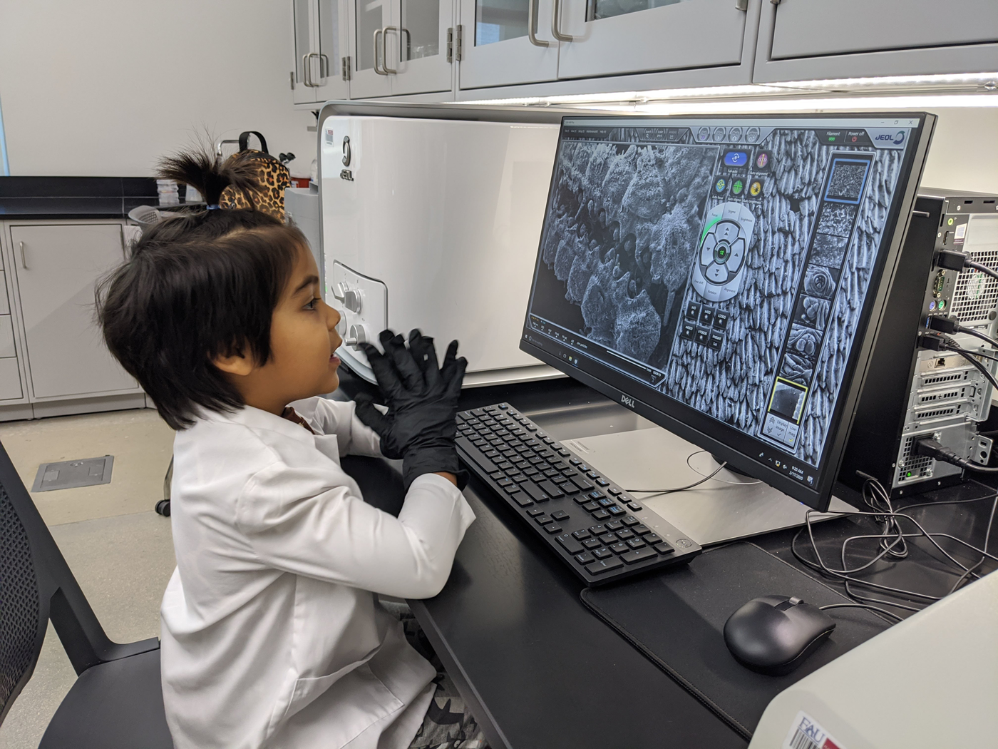
Figure 5: Kindergarten student gets a first look at the JEOL JCM-6000 benchtop SEM at Florida Atlantic University High School Owls Lab (photo courtesy of FAU High School Owls Lab).

Figure 6: SEM image of spider taken using NanoSuit® biofilm for coating biological specimens (photo courtesy of FAU High School Owls Lab). Imaged via JEOL JCM-6000 Benchtop SEM.
Within academic research facilities, users value the flexibility and ease of use that benchtop SEMs provide. Geologic research, for example, often involves characterizing mineral textures and chemistry at the micron scale. For many geologists, non-destructive techniques are paramount for preserving high-value samples such as meteorites. With benchtop SEMs, users can obtain images and chemical data in situ at high resolution, often without the need to add a conductive surface coating (Figure 7). These instruments are applicable to a wide range of other academic research as well, from investigating microfossils that provide information about Earth's past climate, to characterizing the surface morphology and chemistry of cutting-edge climate solutions and beyond.

Figure 7: Geologic thin section of a meteorite (ordinary chondrite, GRO95658). Sample courtesy of NASA and Tim Glotch at Stony Brook University. Meteorites are not conductive and typically require a carbon coat to analyze by SEM/EDS, but given the flexibility of the benchtop system, this montage backscattered electron image was acquired in low vacuum without a conductive coating. Imaged via JEOL JCM-7000 Benchtop SEM.
Conclusion
SEMs are an indispensable tool, and new developments in SEM technology have pushed the limits of what can be analyzed beyond boundaries that existed just a few years ago. With the added convenience of benchtop SEMs, scientists in all aspects of research can increase performance, improve ease of use, and keep the cost at an affordable level. These advantages have made benchtop SEMs a widely available and well-accepted tool across a variety of disciplines.


