


Introduction
The rapid increase in the wireless data demand requires the shift from sub-6 GHz to the millimeter-wave (mm-wave) bands. At sub-6 GHz bands, antennas are usually designed on a PCB due to longer wavelengths and the application-specific integrated circuit front-end systems are then integrated with these antennas with the help of radio frequency (RF) cables and connectors. The resulting solution is not only cost intensive due to use of high-performance RF PCB, but also causes more interconnection losses because of longer feed cables, connectors, and transitions. Besides, the performance of these cables and connectors severely degrades at mm-wave bands. These factors motivate the integration of antennas and front-end chips with a technology that can reduce the interconnection distance and number of transitions [Reference Hsieh, Chu, Ho and Wang1]. The smaller form factor at mm-waves allows the antennas to be placed inside the package, thus making an antenna in package (AiP) solution. The fan-out wafer level packaging (FOWLP) technology has the potential for compact integration of passive and active components [Reference Braun, Becker, Hoelck, Kahle, Woehrmann, Toepper, Ndip, Maass, Tschoban, Aschenbrenner, Voges and Lang2], and in comparison with traditional flip-chip and wire bonding technologies, the FOWLP has shown better electrical performance as well as higher design flexibilities at mm-wave bands [Reference Guan, Fai and Soon Wee3]. Besides, the placement of antenna array in the fan-out (FO) region minimizes the interconnection losses because of least geometrical discontinuities from the chip to the antenna array.
Different FO antennas and antenna arrays are presented at 28 GHz [Reference Hsieh, Chu, Ho and Wang4, Reference Le, Kanitkar, Rossi, Ndip, Braun, Mueller, Lang, Wieland, Goetze, Halim and Trewhella5], 60 GHz [Reference Huang, Dai, Liu, Duan, Wu and Lin6–Reference Nasr, Jungmaier, Baheti, Noppeney, Bal, Wojnowski, Karagozler, Raja, Lien, Poupyrev and Trotta11], 77 GHz [Reference Chen and Zhu12–Reference Fischer, Tong, Hamidipour, Maurer and Stelzer15], and above 100 GHz [Reference Ahmed, Furqan and Stelzer16] where most of the designs use either double molding layers [Reference Hsieh, Chu, Ho and Wang4, Reference Chen, Guan, Wee Ho and Bhattacharya10, Reference Chen and Zhu12], multiple re-distribution layers (RDL) [Reference Le, Kanitkar, Rossi, Ndip, Braun, Mueller, Lang, Wieland, Goetze, Halim and Trewhella5], metallization on top mold [Reference Hsieh, Chu, Ho and Wang4, Reference Le, Kanitkar, Rossi, Ndip, Braun, Mueller, Lang, Wieland, Goetze, Halim and Trewhella5, Reference Chen, Zhu and Zhong7, Reference Tsai, Hsieh, Liu, Yeh, Chen, Hsiao, Chen, Liu, Lii, Wang and Yu9, Reference Chen, Guan, Wee Ho and Bhattacharya10, Reference Chen and Zhu12], through mold VIAs [Reference Hsieh, Chu, Ho and Wang4, Reference Le, Kanitkar, Rossi, Ndip, Braun, Mueller, Lang, Wieland, Goetze, Halim and Trewhella5, Reference Chen, Zhu and Zhong7], or airgap in the mold [Reference Huang, Dai, Liu, Duan, Wu and Lin6]. These variations make the package complex and thus cost-ineffective. Some of the designs implement only a single antenna elements despite the small form factors at 60 and 77 GHz [Reference PourMousavi, Wojnowski, Agethen, Weigel and Hagelauer8, Reference Fischer, Tong, Hamidipour, Maurer and Stelzer13, Reference Ho, Hsieh, Jhong, Kuo, Ting and Wang14]. In this work, a TX and an RX antenna arrays are presented that cover the 26 and 28 GHz bands n258 (24.250–27.5 GHz) and n257 (26.5–29.5 GHz). The arrays are designed at RDL1 using 4 × dipole elements, while the package consists of a single mold and 2 × RDLs. Moreover, a metal backed cavity in the low-cost FR-4 PCB directs the waves in the broadside direction. Furthermore, the presence of active circuits in the module require a heatsink to dissipate the heat, and if the antennas/antenna arrays radiate in the same direction where heatsink is placed, this can significantly degrade the radiation performance of the antenna array. In this work, we have designed a novel horn-shaped heatsink which not only dissipates the heat from the chip but also improves the radiation performance of the antenna array. The beam-steering is achieved in ± 35° in the azimuth plane and the overall measurements verify the simulation results.
The paper is further organized as follows: section “Packaging technology” of the paper briefly discusses the packaging technology used to design the compact antenna array. The design of the antenna array along with novel horn-shaped heatsink is discussed in section “Antenna array design”, whereas section “Fabrication and measurement setup” presents the fabrication and measurement setup used in this work. The performance evaluation is presented in section “Performance evaluation” and section “Conclusion” concludes the paper with the help of a comparison table.
Packaging technology
The traditional packaging process involves dicing the dies from a wafer and then assembling them into a package. The fan-in wafer level package (FIWLP) however assembles a die into a package at the wafer level by using wafer fabrication tools and processes. An RDL is used to connect the I/Os of the chip to the bumps on top of die surface. In the FIWLP, the final package is of the same size as the die itself, thus the technology produces true chip-scale package [17] which can be understood as a bumped die. The FIWLP has advantages of good electrical performance, low cost and small size but a number of applications ask for high number of interconnect bumps under the chip. The FOWLP technology is an enhancement of standard WLPs which solves the interconnect problem of the FIWLP. In the FOWLP, the chips are diced from a silicon wafer and precisely positioned on a carrier panel which is then molded. An RDL then covers the die and the FO area, and solder bumps are connected on the RDL. The idea behind the FOWLP is to introduce a bigger wafer beneath the actual wafer to create bigger die area which has more number of bumps for interconnection and also has an FO area that can be used to place the AiP. In comparison with an antenna array fabricated on an RF PCB, the AiP not only results in reduced interconnection losses but is also a cost-effective solution.
The FOWLP used in this work is an embedded wafer level ball grid array (eWLB) package, presented in Fig. 1. The 0.5 mm ball grid array package comprises of three PSV layers (PSV1, PSV2 and PSV3) and two RDLs (RDL1 and RDL2) [Reference Wu, Dahlbäck, Öjefors, Carlsson, Lim, Lim, Oo, Choi and Yoon18].

Fig. 1. Fan-out wafer level package (FOWLP), containing three passivation (PSV) and two re-distribution layers (RDL).
Antenna array design
A dipole antenna element is used in this work to design a four-element antenna array. For TX and RX, separate but identical arrays are used and they are placed on left and right side of the die as shown in Fig. 2. The arrays are designed on the RDL1 while the transceiver chip feeds the TX and the RX antenna arrays through co-planar waveguide (CPW) lines, shown more clearly in the zoom-in view. The brown circles are dummy solder bumps placed between RDL2 and PCB for mechanical support of the package. The effect of these solder bumps is investigated by using a simple antenna structure and the results show an increase in the dielectric constant of the substrate. When solder bumps are added in the substrate, the resonance moves to lower frequency, which then helps to miniaturize the antenna array. The ground traces in the CPW lines are bridged together through RDL2 layer. Each quarter-wave leg of the dipole is matched to 50 Ω port impedance and fed separately from the chip pads.

Fig. 2. TX and RX antenna arrays placed at RDL1 in the fan-out area of the 12.6 × 12.6 mm2 package. The inset shows the zoom-in view.
Array elements are spaced by pitch p = 3 mm, which is more than the free space quarter wavelength at 28 GHz. Figure 3 shows the simulation results for different values of the pitch. The black curve presents the realized gain for different values of pitch (shown on top x-axis). The realized gain values vary from 9.2 to 9.6 dB and the gain is 9.4 dB for p = 3 mm. The colored curves show the maximum beam-steering range for pitch values between 2.90 and 3.60 mm. The 3 dB beam-steering range is maximum for the pitch p = 3 mm, which is used to design the array in this work.

Fig. 3. Parametric simulations investigating the effect of pitch on the maximum realized gain (black curve with y-axis on the right) and the beam-steering range for different values of pitch (set of colored curves with y-axis on the left).
The mutual coupling between the compact antenna array is a key challenge and to minimize this coupling, a parasitic strip of width 10 μm is employed on RDL2 between every two dipoles. Figure 4 shows the mutual coupling between two outer neighboring legs of the dipole array and it can be seen that the S21 level is significantly reduced when the parasitic strip is in place. This strip plays crucial role in achieving the impedance matching and its placement doesn't affect the radiation performance of the array.

Fig. 4. The mutual coupling between two outer neighboring legs of the dipole array.
Horn-shaped heatsink
A heatsink is a key requirement to dissipate the heat generated by the active circuit in the die. As this heatsink lies in close vicinity of the antenna array, it significantly degrades the radiation performance. Keeping this in view, a novel horn-shaped aluminum heatsink is used which, on the contrary, can improve the radiation performance of the antenna. The heatsink is co-designed with the antenna and thus is a part of the antenna. A cross-section of the heatsink is shown in Fig. 5, which will be screwed on the FR-4 PCB. In the elevation plane, horn has θ = 20° flare angle. Increasing the flare angle to a certain extent can somewhat increase the gain as shown in Fig. 6, but it reduces the overall size of the material which in turn results in reduced heat dissipation capability. A trade-off is made by selecting θ = 20° flare angle. However, in the azimuth plane the beam-steering will be performed and a smaller flare angle can restrict the beam-steering range significantly. Thus 80° flare angle of the horn is designed in the azimuth plane.

Fig. 5. An aluminum heatsink placed on top of the chip package. Reflector backed cavities are also shown in the FR-4 PCB.

Fig. 6. Peak realized gain at 28 GHz for different flare angles (θ) of the horn.
PCB cavity
A reflector backed cavity is designed in the FR-4 PCB at a quarter-wave distance to suppress the back lobe radiation. The array will thus radiate through the mold, away from the PCB. A via fence is used inside the PCB to make the cavity, which is placed in a way that it doesn't interfere with the ground/signal routing from the chip to the PCB.
Reflection coefficients of the antenna array
Ansys Electromagnetics Suite is used to simulate the dipole antenna arrays. As each leg of the dipole is excited through a separate 50 Ω port, looking at Fig. 2, the first element in the array (top dipole) is excited through ports 1 and 2 and port numbers sequentially increment toward the last element at the bottom of figure. As the layout is vertically symmetric, a magnetically symmetric boundary is used in the simulations, and the parametric study in Fig. 7 shows active S-parameters of only four out of total eightports in the array. In the figure, the active S-parameters are plotted in the Smith chart as a function of dipole length. The length l 1 = 2.63 mm (red curve) looks more promising except for S 33, where resistive and reactive parts of the impedance respectively become significantly lower and capacitive. Keeping this in view, l 1 = 2.73 mm is a good trade-off to have all the values below a certain limit. Figure 8 shows the active reflection coefficients for all 8 × ports on the TX side of the package for the final length l 1 = 2.73 mm. The results show < −10 dB impedance bandwidth from 24 to 30 GHz for seven out of the eight ports, while port no. 8 (on bottom) shows values higher than − 10 dB from 28 GHz onward. This is because the package is not fully symmetric keeping in view the ground and signal routing details in the final layout of the package. Except S 11 and S 88 curve pair, it can be seen that all other curve pairs are almost overlapping (S 22 and S 77, S 33 and S 66, S 44 and S 55) because of the symmetricity in the layout.

Fig. 7. Active S-parameters for 4 ports (out of total 8 ports) of the dipole antenna array as a function of dipole length l 1.
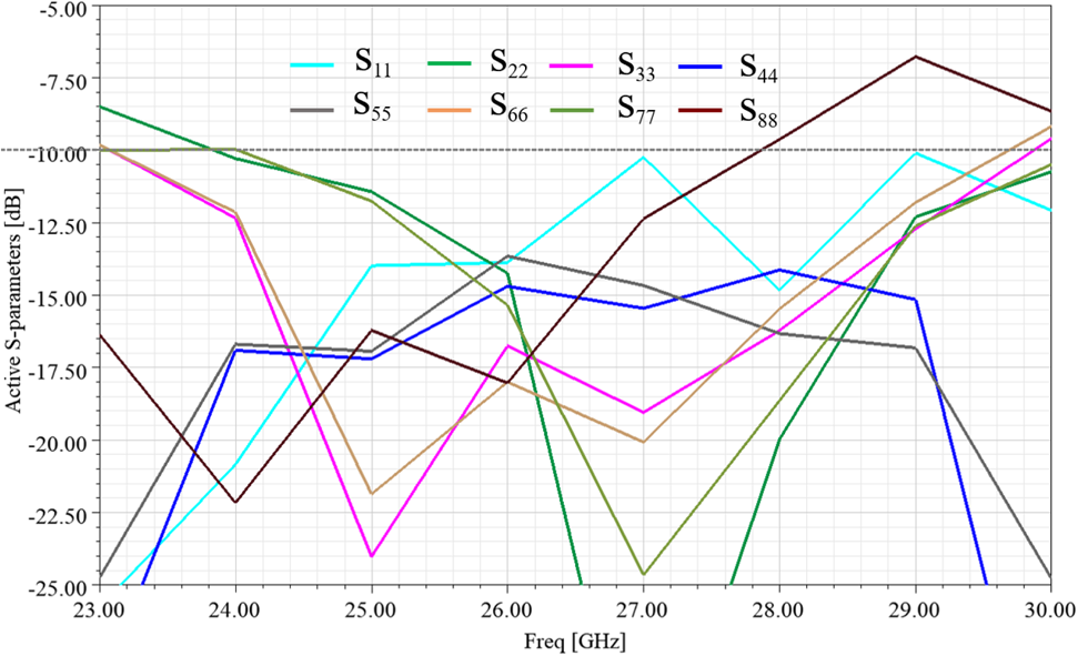
Fig. 8. Active S-parameters for the 4-element dipole antenna array. The eight curves belong to eight dipole legs as each dipole has two legs.
Fabrication and measurement setup
We have designed and manufactured a demonstrator radio frequency module (RFM) for the antenna in package, based on a modified package of the TRX BF/02 RFIC from Sivers Semiconductors. The TX and the RX antenna arrays are fabricated in the 12.6 × 12.6 × 0.8 mm3 package shown in Figs 9(a) and 9(b). Panel (a) of the figure shows the bottom view of the package where the TX and the RX antenna array are placed up and down to the die, respectively. Top view of the package is shown in panel (b) of the figure where die in the middle is surrounded by the molding compound. The wave propagation direction is into the page for panel (a) and out of the page when looking at the panel (b). Figure 9(c) presents the RFM where the package is mounted on an FR-4 PCB and the horn-shaped aluminum heatsink placed on top of the package, and screwed with the PCB. The central ridge of the heatsink sits on top of the die with a thermal interface material between them. The black rectangular regions on both sides of the central ridge are the openings in the heatsink for wave propagation. The top view of the mold can be seen through these regions. An external local oscillator is mounted on the back side of the PCB (not shown in the figure). Panel (d) of the figure presents the evaluation kit designed to characterize the RFM shown in panel (c).

Fig. 9. Fabricated structure: (a) bottom view of the package showing the TX and the RX antenna arrays on RDL1, (b) top view of the package, (c) top view of the radio frequency module (RFM) where package is mounted on an FR-4 PCB and a horn-shaped heatsink is placed on top of the die and is screwed with the PCB, (d) the evaluation kit designed to characterize the RFM.
The schematic diagram of the measurement setup is shown in Fig. 10(a) where the RFM is presented as the device under test (DUT). When evaluating the TX side, the signal generator output is set to 54 MHz, which is passed through a 180° hybrid and each output of this hybrid further goes via a 90° hybrid. The evaluation kit is fed with these four signals IP (in-phase positive), IN (in-phase negative), QP (quadrature-phase positive), and QN (quadrature-phase negative). A power meter is attached to the standard horn antenna on the RX end. The DUT can be rotated in the azimuth and the elevation plane and the horn antenna can be rotated to measure the co- and cross-polarization. The actual measurement setup in an anechoic chamber is shown in Fig. 10(b). All rotations and measurements are controlled by the laptop through the MATLAB scripts.

Fig. 10. Measurement setup: (a) schematic, (b) actual setup.
Performance evaluation
A passive antenna structure is required for complete characterization of the antenna array, however, the manufacturing of a passive antenna structure in the FO eWLB package is an expensive option and is not available. Hence only active measurements are made with the RFIC exciting the dipoles.
Gain and EIRP
Figure 11 presents the peak co- and cross-polarization realized gain as well as peak effective isotropic radiated power (EIRP) versus frequency of operation. Black and red tick mark labels on left y-axis in the graph presents the co- and cross-polarization peak gains, respectively. The polarization isolation is around 25 dB or more for the band of interest. Besides, the absolute values of simulated co-polarization peak realized gain (left black y-axis) and peak measured EIRP (right y-axis) can not be compared as the EIRP also involves the gain from the chip, however, the curves show the same trend with the frequency. The detailed EIRP measurement is shown in Fig. 12 different frequencies when input power of the 54 MHz signal is increased gradually from − 20 to + 18 dBm. The maximum measured EIRP is 34.3 dBm at 28 GHz. The values are minimum for 24 GHz which is in accordance with the peak realized gain simulated results presented in Fig. 11. The maximum EIRP values stretch in 4.6 dB range for 24.00–29.50 GHz band, however, this range reduces to 1.6 dB if 24 GHz curve is overlooked.

Fig. 11. Simulated co- and cross-polarization peak realized gains (left y-axis) and measured peak EIRP (right y-axis) versus frequency of operation.

Fig. 12. EIRP measurements for different frequencies when input power is swept from − 20 to + 15 dBm in 1 dBm steps.
Radiation patterns
The radiation pattern measurements are compared with the simulation results at 28 GHz in Fig. 13. The measurements agree with the simulations for both azimuth and elevation plane. For the elevation plane, co- and cross-polarization radiation pattern measurement results are presented in Fig. 14 for frequencies 24.00–29.50 GHz. The polarization isolation is more than 25 dB for all frequencies, which verifies the simulation results presented in Fig. 11. Besides, in the azimuth plane, the beam-steering is performed by providing different weights to each dipole in the array. The measurements results for beam-steering are presented along with their simulation counterparts for 28 GHz in Fig. 15. Panel (a) shows the simulations, while panels (b) and (c) of the figure present the measured beam-steering results for the RX and the TX, respectively. The main beam is steered in ± 35° in the H-plane, while keeping the peak level above − 3 dB. The measured results look in good agreement with the simulations.

Fig. 13. Azimuth and elevation plane radiation pattern measurements at 28 GHz in comparison with the simulation results.

Fig. 14. Elevation plane radiation pattern measurements for different frequencies in co- and cross-polarization.

Fig. 15. Beam steered radiation pattern in the azimuth plane (H-plane) at 28 GHz: (a) simulated, (b) measured RX, (c) measured TX.
Error vector magnitude
Figure 16 shows the error vector magnitude (EVM) measurements for an EIRP sweep from 15 to 30 dBm. The measurements are made with the help of Keysight N9040B UXA Signal Analyzer (2 Hz–50 GHz) at different temperatures, which is controlled through a Thermotron environmental test chamber. The measurement are made using modulation and coding scheme 24 (MCS24) with 64 QAM (quadrature amplitude modulation). The 30 dBm EIRP is achieved for EVM < −15 dB. The spread in power at a fixed EVM is up to 5.4 dB. Besides, as also seen in the previous simulations and measurements, the 24.00 GHz is the least performing and has lowest EIRP at a fixed EVM value.

Fig. 16. Error vector magnitude (EVM) versus EIRP measurements for different junction temperatures.
Conclusion
This paper presents a four-element compact dipole antenna array designed using single mold FOWLP technology. The RFM shows 34.3 dBm peak EIRP with beam-steering in ± 35° range. A comparison with the similar reported work at 28 GHz is presented in Table 1. The work reported in [Reference Hsieh, Chu, Ho and Wang4, Reference Le, Kanitkar, Rossi, Ndip, Braun, Mueller, Lang, Wieland, Goetze, Halim and Trewhella5, Reference Watanabe, Ali, Zhang, Ravichandran, Kakutani, Raj, Tummala and Swaminathan19] uses multiple RDLs and double molding layers in comparison to this work which uses 2 × RDLs and a single molding compound. Moreover, this work demonstrates the beam-steering in ± 35° in the azimuth plane. Keeping in view the performance of the array, the proposed solution is a good candidate for both n258 (24.250–27.5 GHz) and n257 (26.5–29.5 GHz) bands.
Table 1. Comparison with the similar reported work at 28 GHz

Acknowledgements
This work has been funded by the Swedish research agency Vinnova for development of 5G RFIC integrated with antenna array solution, through project number: 2018-01559. Besides, we are thankful to Mirpur University of Science & Technology (MUST), Mirpur, Pakistan, for financial support of Imran Aziz. Besides, we acknowledge Björn Franzen's help in the measurements.
 Imran Aziz received his B.Sc. and M.Sc. degrees in Electrical Engineering from University of Azad Jammu and Kashmir, Muzaffarabad, Pakistan in 2007 and 2013. He completed his Ph.D. in Microwave Engineering in 2021 from Uppsala University, Sweden. Between 2007 and 2012, he worked in Special Communications Organization (SCO) as Communication Engineer and in Huawei Technologies as GSM BSS Engineer. In 2012, he joined Mirpur University of Science and Techonology (MUST), Mirpur Azad Jammu and Kashmir, Pakistan, as Lecturer in the Department of Electrical Engineering. His research interests include antenna arrays design, fabrication and measurements, millimeter-wave propagation, and front-end systems for beam-steering applications. During his Ph.D., he has remained involved in different projects at millimeter-wave bands, and the outcome of those projects has found its place in the commercial market. He has also worked on the development of 60 GHz wireless interfaces for different harsh environment applications ranging from cryogenics to data read-out in irradiation environments at CERN.
 Dapeng Wu received his M.Sc. degree in Wireless and Photonics Engineering from Chalmers University of Technology, Sweden in 2016. Since 2016 he is an RF engineer at Sivers Wireless AB, Sweden. His current research interest is in eWLB package design.
 Erik Öjefors (S’01-M’06) received his M.Sc. degree in Engineering Physics and his Ph.D. degree in Microwave Technology from Uppsala University, Sweden, in 2000 and 2006 respectively. In 2007 he joined the Institute of High-Frequency and Quantum Electronics at the University of Siegen, Germany. Between 2008 and 2011, he was with the Institute for High-frequency and Communication Technology at the University of Wuppertal, Germany. Since 2011, he is a Senior RF Engineer with Sivers IMA AB, Kista, Sweden. He was the co-recipient of the 2007 IEEE AP-S R. W. P. King Award, the 2008 EuMIC Best Paper Award, and the 2010 EuMC Microwave Prize.
 Johanna Hanning was born in Sweden. She received a M.Sc. in Engineering Physics and in Wireless and Photonics Engineering in 2012, and the degree of Licentiate of Engineering in Microtechnology and Nanoscience in 2016, from Chalmers University of Technology, Sweden. Hanning is specialized in millimeter wave and terahertz technology and her current research interest is in RFIC-based millimeter wave modules for CPE and FWA applications. Since 2019 she holds the position of RF Design Engineer in the R&D department at Sivers Wireless AB, Sweden.
 Dragos Dancila graduated as an Electrical Engineering (magna cum laude) from Université catholique de Louvain, Belgium, in 2006 and received in 2011 the Ph.D. degree in Microwave Engineering from the same university, on a research topic related to RF-MEMS and microfabrication technologies for millimeter-wave components, research which was realized at IMEC, Belgium on a prestigious FRIA grant of the National Science Foundation (FNRS). At Uppsala University, he became Docent in June 2018 and Associate Professor in March 2019. He was project leader for Uppsala University in different national and European level projects. He is presently leading the Microwave Group. He is author or co-author of more than 90 publications including journals and conferences. He is presently teaching electronics and microwave engineering courses at Uppsala University. Deputy Section Editor of IET's Journal of Engineering. His research is conducted in the areas of millimeterwave antennas, reflectarrays, RF sensors and at the FREIA laboratory, on high-power RF and microwave amplifiers and material processing using high-power microwaves. Dragos has also a formal education in Business Management from Solvay Business School in Brussels and is founder of the company Percyroc AB.


 Open access