Introduction
Materials characterization methods can seem like an alphabet soup of three- and four-letter acronyms. Three common microscopy-based methods capable of providing nanoscale morphology information are discussed. The approach here is from a practical end-user perspective, trying to understand which technique is best suited for a given application or sample. In this article we examine scanning probe microscopy/atomic force microscopy (SPM/AFM), scanning electron microscopy (SEM), and transmission electron microscopy (TEM). This overview first compares and contrasts AFM and SEM with respect to their operating principles, capabilities, and resolution as well as important practical considerations such as sample preparation and the sample environment within the microscope. Since its introduction in 1986, the terms “scanning probe microscopy” and “atomic force microscopy” often have been used interchangeably. For simplicity this overview refers to these methods only by the acronym AFM. The overview concludes with a similar summary of TEM.
Comparing SEM and AFM Operating Principles
Scanning microscopy
Both SEM and AFM rely on scanning to form an image that is built up line by line as a probe scans the surface in a raster pattern. That is where the similarity ends. The fact that one method uses electrons to probe the surface while the other uses a sharpened tip dictates important differences in the physical construction of each microscope, the nature of the specimens examined, and the kind of information that can be extracted. Figure 1 schematically describes some of the key elements of an SEM and an AFM.
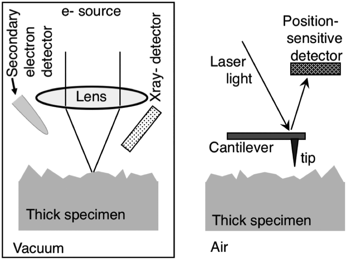
Figure 1: Key instrumentation elements associated with SEM (left) and AFM (right).
SEM
Electron microscopes typically use either a thermionic or field-emission electron source. Thermionic sources are less expensive and can operate under easily accessible high-vacuum conditions. A field emission source, often referred to as a field-emission gun (FEG), can produce higher image resolution and has a much longer lifetime, but it requires more stringent vacuum conditions.
Lenses in an SEM are used to focus a beam of electrons to a small point on the surface of a specimen. Electron microscopes typically use magnetic fields for focusing, and focusing simply corresponds to changing the current going through the electromagnet producing the field. A set of electromagnetic scanning coils is used to raster the focused electron beam over the specimen, while a variety of signals may be collected during that raster to produce contrast and form an image.
AFM
The AFM forms an image by a very different operating mechanism. The heart of the scanning probe microscope is a small (often silicon) cantilever with a sharp tip pointing down toward the specimen surface. Cantilever dimensions are similar to those of a human hair. The tip is generally cone-shape with a tip radius of curvature of ∼10 nm. Depending on the instrument design, either the specimen or the probe is raster-scanned in order to measure topography. As the tip is deflected by small forces at the surface, a myriad of surface properties, including mechanical and electrical, can be measured. Laser light is reflected off the back of the cantilever to a position sensitive detector (PSD), which tracks cantilever motion as the tip interacts with the surface.
Resolution
One of the key advantages of both AFM and electron microscopy (EM) techniques is that they can achieve much higher resolution than traditional light-optical microscopes (LOMs). The resolution of a standard LOM is in the range of 0.2 µm to 1 µm. In contrast, AFM and EM can provide resolutions ranging from about 0.1 nm to 10 nm depending on the technique and how it is used.
The image resolution of an SEM is about 1–10 nm. It is determined by a balance between the electron wavelength and aberrations associated with the electromagnetic lenses. The electron wavelength in an SEM is much smaller than that of the visible light used in an LOM. However, in contrast to light microscopes, where the wavelength of light limits image resolution, typical SEM image resolution is limited by uncorrected aberrations and effects from the electron beam-specimen interaction.
AFM has different resolution in the lateral (x,y) and vertical (z) dimensions. The lateral resolution in conventional AFM operating modes depends primarily on the dimensions of the tip apex and the surface properties of the specimen. On a soft sample, for example, the tip can depress further into the surface, resulting in a lower resolution relative to that of a stiff surface. Generally, AFM can achieve at least 5–10 nm lateral resolution. This resolution can be significantly improved with more sophisticated imaging modes on certain samples, even attaining atomic resolution in some cases. Since the deflection of the cantilever can be precisely measured, the vertical resolution can be at the sub-nm level, significantly higher than its lateral resolution.
Field of view
Although both SEM and AFM are scanning-based methods, they vary greatly in screening capability and acquisition speed. SEM has a clear advantage over AFM in surveying large areas because it is capable of scanning millimeters of surface area in just a few images. In contrast, the AFM can only image a maximum of approximately 100 μm × 100 µm at a time.
Acquisition speed
In terms of the time required for image acquisition, the SEM is currently faster, but AFM is quickly gaining ground. Once the image parameters are optimized, SEM image acquisition takes only about a minute or less. In contrast, collecting a high-resolution AFM image requires approximately 5–10 minutes. Vendors have been making significant progress decreasing AFM acquisition times on some higher-end research systems reaching video rate imaging speeds in some cases.
Image formation
Both SEM and AFM raster a probe across a surface. In each case, the probe—whether it is a focused electron beam or a sharp tip—is positioned at a specific point (pixel) on/over the specimen and held there for a user-selected dwell time (typically μsecs to msecs). During the dwell time, one or more signals are collected before the probe is moved to the next pixel, the distance of which is called the interpixel spacing. The line-by-line x-y rastering forms a two-dimensional image.
In SEM, the magnification is determined by the x-y dimensions of the image on the viewing monitor divided by the x-y dimensions of the physical raster on the specimen (Figure 2). In AFM, the magnification is determined by the scan size set by the user. The SEM and the AFM share another user-defined parameter, pixel resolution, which can range from low resolution (for example, 128 × 128 pixels) to high-resolution (2048 × 2048 pixels) for a given scan size. Contrast within the image is determined by the nature of the signals collected at each pixel position and how these signals vary from pixel to the next with the topography and/or physico-chemical properties of the specimen.
Operating Modes
AFM modes
There are dozens of AFM modes that probe various material properties in addition to topography such as mechanical (adhesion, stiffness, friction), magnetic (magnetic forces, domains), and electrical (conductivity, surface potential, electrostatics). All these modes are variations of a few key operating modes. The most common mode, often referred to as “tapping mode,” oscillates the cantilever at its fundamental resonance frequency and intermittently taps the surface to map 3D topography and generate contrast related to variations in material properties.
The AFM can also conduct single-point measurements where a force vs. displacement curve is collected over the full tip-sample interaction as the probe approaches, pushes into, and then retracts from the sample. These kinds of measurements are referred to as “force spectroscopy” where the curves can be analyzed for useful data on material properties. For many electrical and magnetic properties, the AFM relies on a specialized mode where the AFM probe makes two passes over every line as it raster scans. One pass is for topography, and a second pass occurs at a prescribed height with either a DC or AC bias voltage to probe electrical interactions.
SEs and BSEs in the SEM
A typical SEM collects at each pixel position either or both of two different electron signals. Secondary electrons (SEs) constitute the most common signal, particularly for revealing surface topography over a wide range of magnifications (Figure 2). Secondary electrons have low energies (less than 50 eV), and they can be collected using a secondary electron detector biased with a positive voltage that attracts the SEs (see Figure 1). A second SEM imaging signal comes from backscattered electrons (BSEs). The BSE signal corresponds to incident electrons whose trajectories are reversed by the sample such that they escape from the surface. The BSE signal is best collected using a detector located just below the final SEM lens. The BSE intensity depends primarily on the local average atomic number. Heavier elements have higher positive charges in their nuclei and cause greater numbers of backscattered electrons than light elements. Hence, the BSE signal is particularly good at differentiating specimen regions with different average atomic numbers (see Figure 3). Importantly, BSEs collected with an overhead detector are not very sensitive to sample topography.
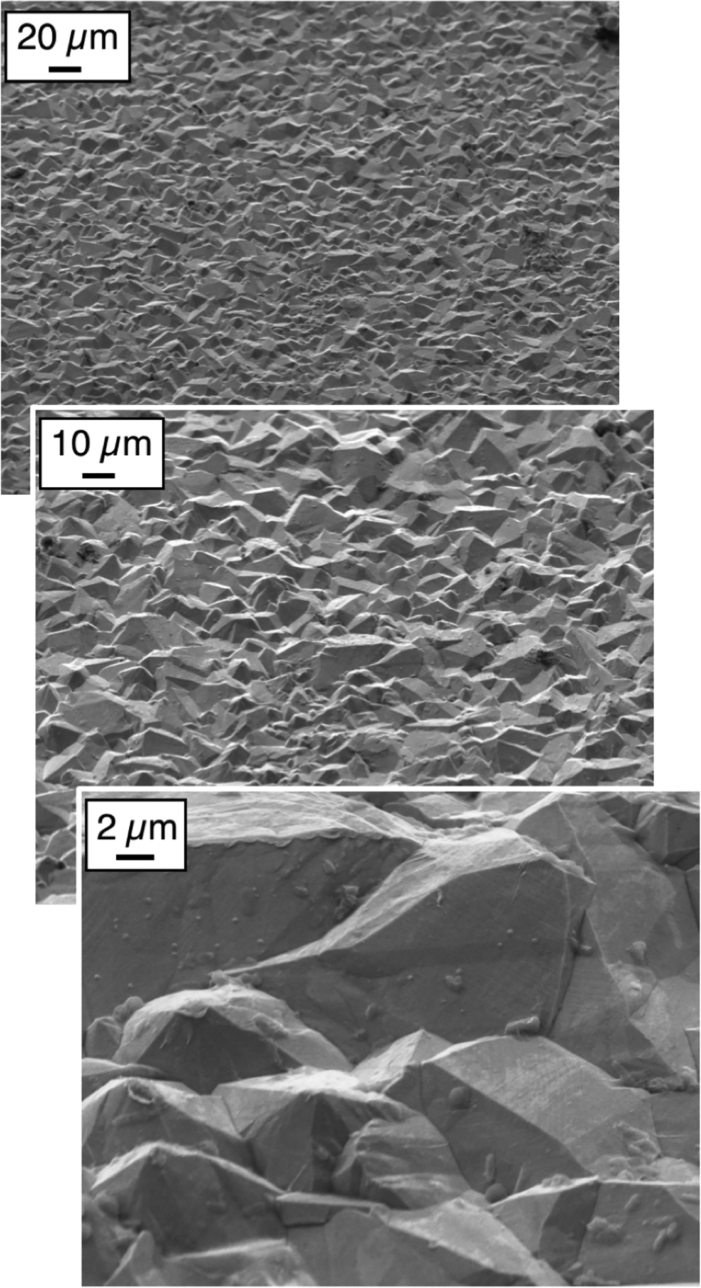
Figure 2: Secondary electron SEM image of a rough metal surface from low (top) to high (bottom) magnification. Secondary imaging allows rapid image acquisition over large fields of view with easy control over magnification.

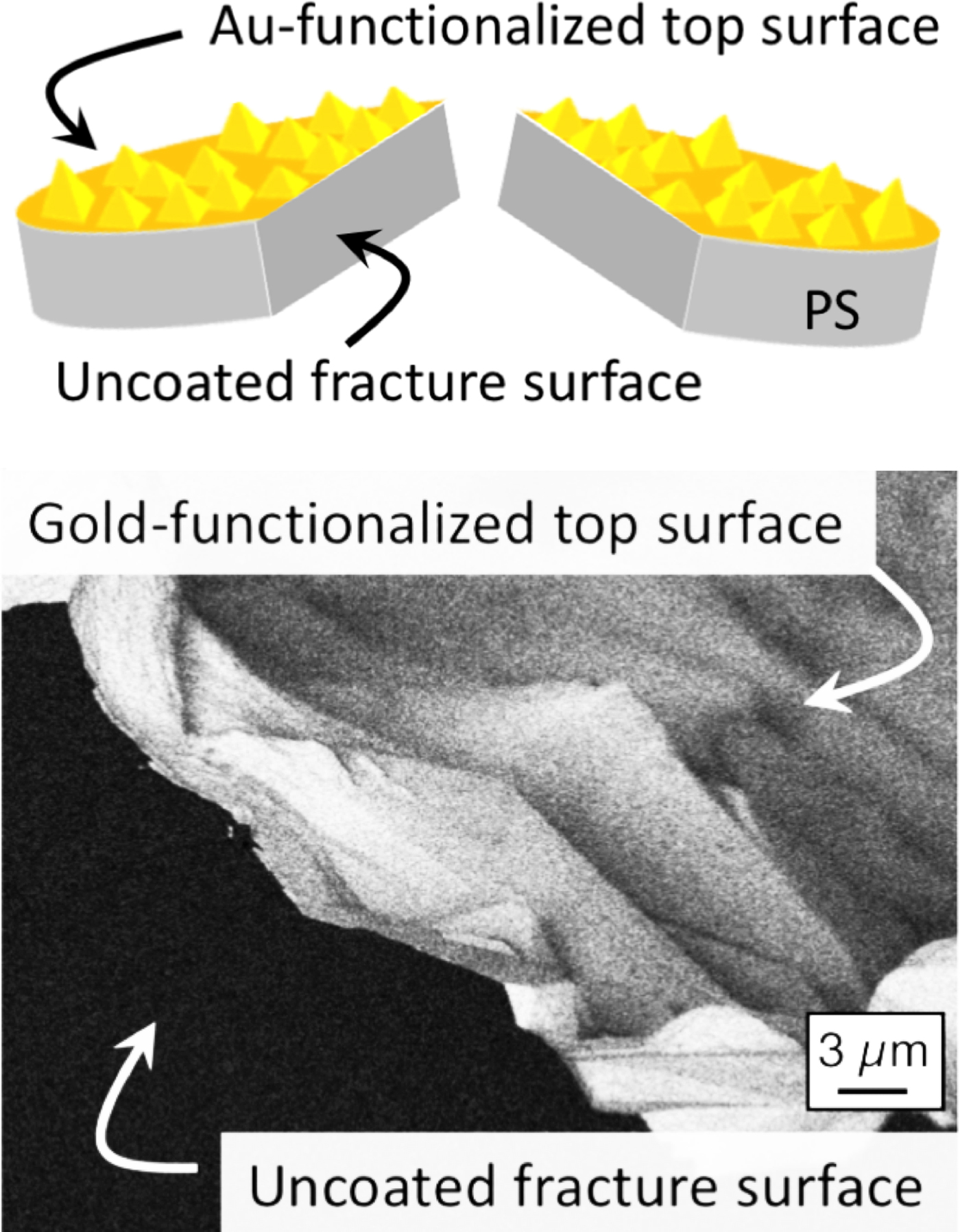
Figure 3: Backscattered SEM image of a gold-functionalized nano-rough coupon of polystyrene (PS) after fracturing (see top schematic). The backscattered-electron image shows bright contrast on the top surface where the high-atomic-number gold layer is located but dark contrast on the uncoated polymer (low atomic number) fracture surface.
Sample Environment
To decide whether to use SEM or AFM, an important early question centers on the conditions under which the sample will be imaged: vacuum, ambient, or fluid. The environment does not matter much for many samples such as semiconductors, metals, or geological samples, but some studies need to occur under fluid. This might be true for a biological specimen, a hydrated polymer, or a sample with a thin oil film.
SEM
Electron microscopes require a vacuum for the electron beam because electrons are scattered by gas molecules (O2, N2, etc.) as they travel from the electron source to the sample. This vacuum requirement means that the standard electron microscope cannot work with wet samples or with samples that contain a component with a high vapor pressure (for example, insufficiently cured epoxy). There are specific EM techniques that overcome this constraint. Cryo-electron microscopy, for example, freezes hydrated specimens and keeps them frozen during analysis. Also, the so-called variable-pressure SEM enables imaging when sample chamber vacuum conditions are in the range of 0.01 to 20 torr. Similarly, special sealed sample holders are available to allow samples for SEM or TEM to be held in a small volume of liquid. These are specialized methods, however, requiring additional instrumentation, which adds complication to the basic imaging procedure.
AFM
The AFM holds a significant advantage over SEM with respect to the sample environment. It can operate in air or fluid under ambient conditions—no vacuum required. Experiments where samples are immersed in fluid are especially popular in the biological community, which strives to conduct in situ studies of cells and tissues. Atomic force microscopes have even been placed in glove boxes and operated under controlled environments with respect to humidity and nitrogen/argon environments for applications such as battery research.
Sample Preparation
Regardless of the microscopy method, good imaging requires well-prepared samples. A common mistake is to wait until the end of a large project to pursue some microscopy. At that point, creating an appropriate sample can often be difficult and costly. In contrast, thinking about specimen requirements early can enable good samples to be created within the natural workflow of the overall project.
AFM
Atomic force microscopy poses minimal constraints on the sample, provided that it is relatively flat. The allowable sample size depends on the instrument design. Some instruments are designed for large samples such as 300 mm silicon wafers, while high resolution instruments might only handle samples that are up to 15 mm in diameter and a few mm thick. Samples also need be smooth to be within the z range of the piezo, which is typically 5 µm. A few AFM instruments support a larger z limit of 15 µm, and these are used mostly by the biological community. In contrast to samples for the SEM, there are no constraints on the electrical conductivity of the samples that can be run on an AFM.
SEM
Like an AFM, the sample size for an SEM depends on the microscope itself. Typical SEMs can accommodate a sample about the size of a hockey puck, though smaller is better. Some microscopes are designed specifically for large samples, such as silicon wafers or broken engine components for failure analysis.
The SEM has another differentiating feature possessed by no other microscopy method, namely, a large depth of field. Thus, in addition to imaging smooth samples, an SEM can image very rough samples. Fracture surfaces encountered during a failure analysis, for example, often have roughness values ranging from micrometers to millimeters. An SEM can often obtain images in these situations where both the peaks and the valleys are in focus simultaneously.
Electrically insulating samples (for example, polymers and ceramics) often present particular challenges to SEM analysis since they tend to accumulate surface charge from the impinging electron beam. In such cases, samples are typically coated with a very thin layer (2–10 nm) of a conductive material such as sputtered gold-palladium alloy. Alternatively, an SEM with a FEG electron source may be operated under so-called low-voltage conditions (∼1 kV) where uncoated insulating samples tend not to charge. Again, the AFM has no constraints from the electrical properties of the sample. Thus insulating, semiconducting, and conducting samples are handled with the same ease by the instrument.
Other Characterization Information
Quantitative height measurements
One of the AFM's differentiating capabilities is its ability to go beyond two-dimensional x-y imaging by quantitatively measuring small height (z) differences with high precision. As mentioned above, the vertical resolution of height differences in AFM is sub-nanometer. Figure 4 shows a topographic AFM image of a thin, solid inorganic lubricant film generated to reduce friction between two surfaces. This film has a lot of texture with many peaks and valleys that are easily visualized and quantified in the AFM image. The film's morphology directly affects its friction reduction capabilities, so a quantitative measurement of its topography is essential for evaluating its performance. In contrast, the SEM does not provide any quantitative height information.
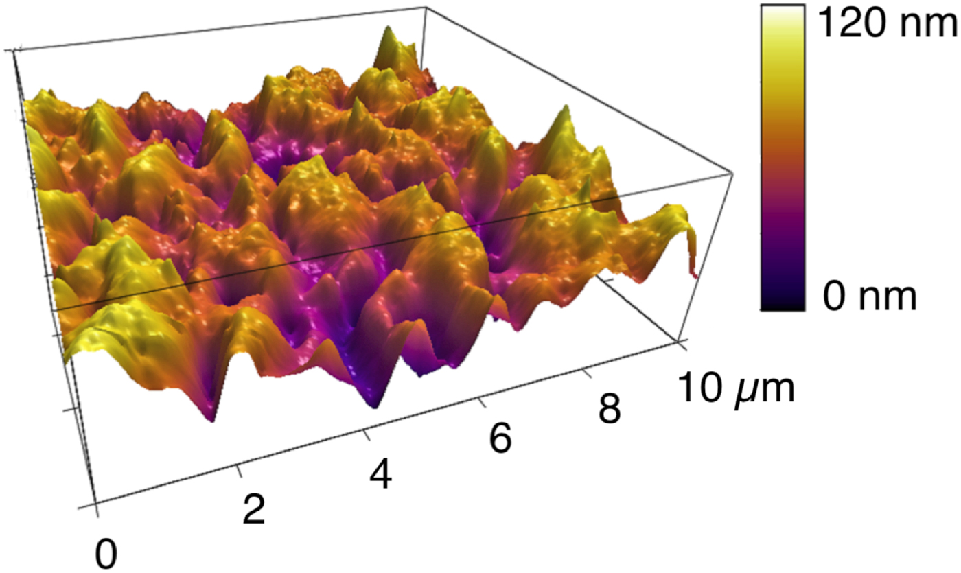
Figure 4: AFM topography image of a lubricant boundary film, formed under high temperature and pressure conditions. The friction reduction properties of such films depend on its morphology and thus the ability to quantify its roughness is key to understanding its performance. The RMS roughness of this film is 17.3 nm.
Compositional analysis
Compositional information can be critical to a full characterization of a material, particularly for the correlation of surface properties to performance in a wide array of applications. With the addition of an X-ray spectrometer to the SEM, the user can obtain elemental composition either through point measurements or elemental mapping.
SEM
The most common way to extract compositional information in an electron microscope exploits the fact that X-rays are emitted from atoms in the sample when an electron beam hits the surface. These X-rays can be collected using an energy-dispersive spectrometer (EDS), where the X-ray intensity is measured as a function of its energy (Figure 5). Different elements emit X-rays with specific energies. These are called characteristic X-rays because they reveal the identity of each element. Almost all EDS systems can detect elements heavier than sodium, and many modern systems can detect elements as light as boron. Importantly, EDS measurements in an SEM can be made with high spatial resolution (∼ 0.1 μm–1 µm, depending on the energy of the primary electron beam) because the incident electron beam is focused to a fine probe. Furthermore, since the focused electron beam can be digitally rastered over the specimen, X-ray data can be collected at each pixel to produce 2D maps showing the distribution of individual elements across the field of view.
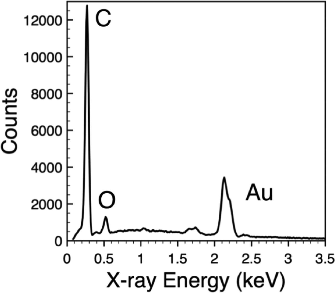
Figure 5: Energy-dispersive (EDS) X-ray spectrum collected from polycaprolactone (PCl) nanofibers decorated with gold (Au) nanoparticles. Peaks in the spectrum correspond to carbon (C) and oxygen (O) X-rays from the PCl and Au X-rays from the nanoparticles.
With the addition of an electron backscatter diffraction (EBSD) system, an SEM can identify the orientation of individual grains of a polished specimen of metal or mineral. The weak diffraction pattern emitted from an inclined specimen is analyzed with computer software to provide the orientation of any crystal grain in a polycrystalline material. This method may be used for producing grain orientation maps of a polycrystal, for phase identification, and for strain analysis.
AFM
AFM does not make specific measurements of composition, but it is a powerful tool to obtain contrast based on material properties, which in turn are related to material composition. For example, a heterogeneous sample may be topographically flat with different domains that are chemically similar and thus difficult to differentiate by traditional imaging methods. However, AFM can differentiate such domains successfully if there are differences in stiffness, adhesiveness, viscoelasticity, or dissipation between the materials. This scenario occurs frequently for phase-separated polymers and polymer composites. The most common AFM mode for material-property contrast is called phase imaging, where the phase lag (or lead) between the driven cantilever and its response is measured. The material contrast in phase imaging derives from a convolution of material properties locally on the specimen surface.
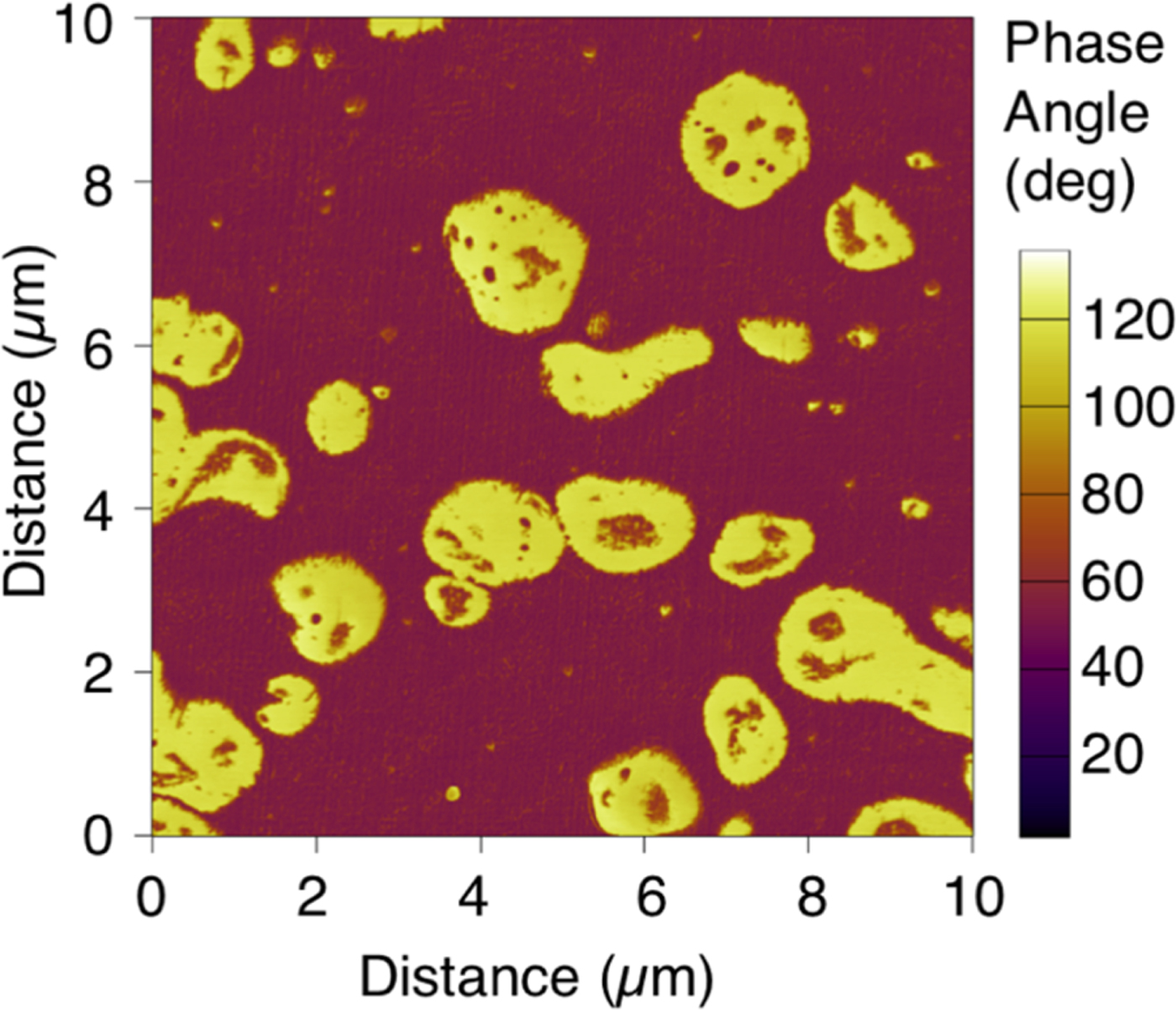
Figure 6 shows a 10 μm × 10 µm AFM phase image of a blend of polypropylene and rubber. Although the polypropylene (purple) and rubber (yellow) are chemically similar, the phase image easily differentiates them based on their mechanical properties. With such a contrast mechanism, the morphology, dispersion, and distribution of the phases in this material are easily visualized and quantified.

Figure 6: AFM phase image of a blend of rubber domains (yellow) and polypropylene matrix (purple). While the two materials are chemically similar, their mechanical properties—especially adhesion and stiffness—vary significantly, enabling easy differentiation with the AFM.
Conventional AFM has no ability to provide elemental or crystallographic information. However, recently developed instrumentation integrates infra-red (IR) spectroscopy with AFM to provide IR spectroscopic information on the 10–100 nm length scale. There are currently two operating principles through which AFM-IR can be collected. The first involves a photothermal measurement where the sample heats up, knocks against the cantilever, and the cantilever ringdown is measured and related to the IR spectrum. The second involves a near-field scattering based method, where the cantilever acts as an antenna to focus the IR light at a localized point underneath the probe. These nano-IR methods can provide a full vibrational spectrum at a single pixel point, or map the vibrational amplitude at a given frequency over an entire image. Additionally, hybrid methods that join AFM with confocal Raman spectroscopy are also commercially available where the Raman spectrum is collected from the same area (although with significantly less spatial resolution) as imaged by the AFM.
Mechanical and electrical properties
Because of sample-tip interactions, the AFM is particularly well suited to probe nanoscale mechanical and electrical properties. The AFM can quantify at high spatial resolution both elastic and viscoelastic materials. These techniques rely on force spectroscopy-based methods, where the force vs. displacement is tracked at each pixel, as the tip approaches and retracts from the sample. These curves are then fit to appropriate contact mechanics models in order to extract properties such as adhesion or static (Young’s) modulus. Recently, methods to probe viscoelastic properties such as storage modulus, loss modulus, and loss tangent have also been developed.
In addition to mechanical properties, AFM also can measure nanoscale electrical and magnetic properties. Electrical measurements include those for surface charge, current, capacitance, surface potential, and conductivity. These methods typically require the use of electrically conductive probes and the 2-pass mode described above. Note that, except in special cases, electron microscopes do not have a means to provide direct measurements of local mechanical or electrical properties. In some cases, an AFM can be incorporated within the EM itself to make correlative measurements of morphology and local materials properties.
Transmission Electron Microscopy (TEM)
A TEM can provide information not accessible by SEM or AFM, but it brings additional operational complexity and more stringent requirements on specimen preparation. Electrons interact much more strongly with matter than light or X-rays, and this means that TEM specimens must be extraordinarily thin in order for the electrons to be transmitted through the specimen to the detectors. Sample thicknesses must be less than about 100 nm, depending on the material. Thin sections of soft materials can be cut using ultramicrotomy, which can be extended to include cryo-ultramicrotomy if the sample is hydrated or has a low glass transition temperature. Thin sections of hard materials—metals, ceramics, and semiconductors—can be prepared by precision grinding, chemical- or electro-polishing, or by focused-ion-beam (FIB) micromachining. In addition to the important constraint on specimen thickness, a standard TEM sample must be 3 mm in diameter in order to work with the specimen holders of most commercial TEMs.
Perhaps the most distinguishing feature of a TEM is its ability to obtain electron diffraction patterns from regions about 1 µm in diameter and smaller. By itself, diffraction enables detailed crystallographic studies to be pursued. For example, a TEM can collect diffraction data to determine the relative orientations of different grains in a polycrystalline material or to identify the crystal structure of a precipitate particle in some continuous matrix phase. Pre-specimen and post-specimen electron optics allow portions of diffraction patterns to be converted into images. Thus, for crystalline materials, diffraction-contrast imaging is the most commonly used TEM imaging mode. An image formed using only the transmitted (undiffracted) beam is called a bright-field image (Figure 7), and an image formed using one of the diffracted beams is called a dark-field image. The specialized technique referred to as high-resolution electron microscopy (HREM) combines the transmitted and diffracted beams in a manner that often allows individual atoms to be resolved.
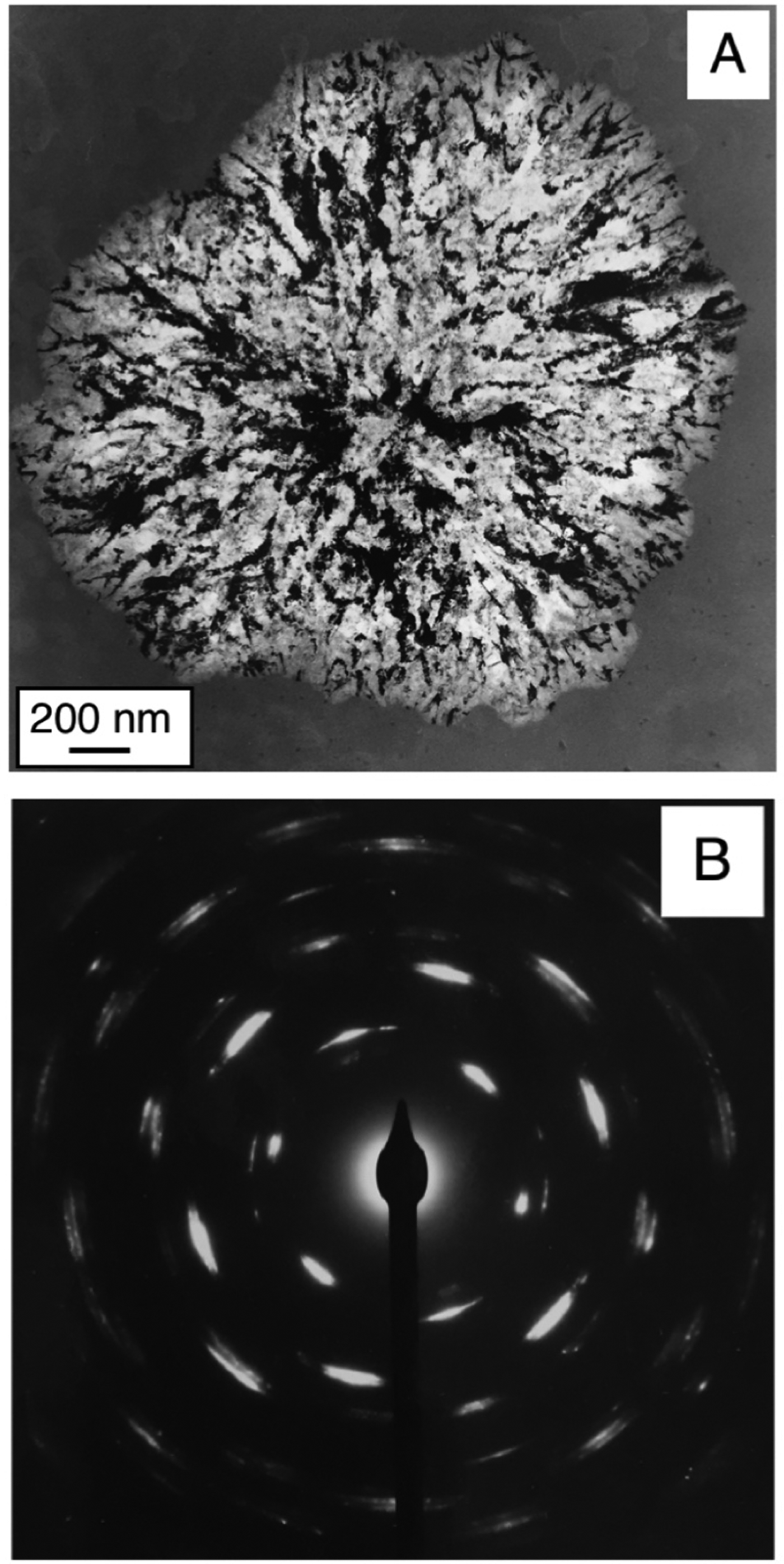
Figure 7: (A) Bright-field TEM image showing the crystallization of an amorphous Ge-Te thin film (∼70 nm thick). The brighter regions transmit most of the incident electrons, while the darker regions diffract most of the incident electrons. (B) An electron-diffraction pattern from the crystal in (A). The central (transmitted) electron beam is partially blocked by a beam stop placed just before the camera. The other bright spots each correspond to a beam of electrons diffracted from the crystal. The distance of each spot from the center gives information about the spacing between adjacent atomic planes. The relative positions of the spots give information about the type of unit cell for a germanium telluride crystal. The fact that each spot is elongated into a small arc indicates that light and dark regions in image (A) contain many crystalline defects.
Like an SEM, the incident electrons in a transmission microscope generate X-rays, and these X-rays can be measured to extract compositional information using much of the same EDS instrumentation and data analysis methods used in the SEM, but the compositional information has higher spatial resolution (∼1 nm–20 nm). With the addition of an electron spectrometer, the TEM has the additional capability of doing electron energy-loss spectrometry (EELS) to provide further chemical information. The number of electrons at each value of energy loss may be plotted to give a spectrum of the electrons that have lost energy as they passed through the thin sample. Again, this information comes from the region of the sample illuminated by the electron beam, so it can be of high spatial resolution (∼1–20 nm). In addition to providing compositional information, EELS can also provide information about the chemical bonding within a sample. The EELS spectrum is useful in studying materials comprised of light elements (C, N, O, etc.) and is often used for studies involving ceramics and polymers.
Acknowledgments
Much of Matthew Libera's research efforts associated with electron microscopy have been supported over many years by the Army Research Office (most recently by grant # W911NF-17-1-0332) and by the National Science Foundation (most recently by grant # DMR-1827557).